
Sheet resistance variation of graphene grown on annealed and mechanically polished Cu films
Jong-Kwon Leea,
Chang-Soo Parkb and
Heetae Kim*c
aGlobal Frontier Center for Multiscale Energy System, Seoul National University, Seoul 151-744, Republic of Korea
bDepartment of Physics, Hanyang University, Seoul 100-715, Republic of Korea
cRare Isotope Science Project, Institute for Basic Science, Daejeon 305-811, Republic of Korea. E-mail: kim_ht7@yahoo.com; Tel: +82-42-878-8823
First published on 4th November 2014
Abstract
Graphene was grown on a Cu film, processed by annealing and mechanical polishing. The sheet resistance of graphene shows ∼57% decrease by mechanical polishing for raw Cu and ∼20% decrease by annealing for 50 nm SiO2 polishing.
Graphene, the two-dimensional hexagonal lattice of sp2 hybridized carbon atoms, shows superior mechanical, thermal, electronic and catalytic properties.1 These unique properties make graphene suitable for electronic, photonic, energy and analytical applications.2–7 For commercializing the graphene-based devices, it is crucial to synthesize and transfer large-scaled graphene films on various substrates. Thus, chemical vapor deposition (CVD) growth on metal film catalysts such as copper, nickel, ruthenium and iridium8–11 became one of the most promising methods, because CVD can fabricate transferrable high-quality graphene films with a large area of 30 inches.12 Moreover, there has been a lot of research on developing the fabrication processes of CVD-graphene and investigating its properties such as crystallinity, resistivity and functionalization.13–15
Particularly, Cu as a substrate is attractive because of its low carbon solubility and surficial self-limiting regime when used for graphene synthesis.16 Thus, graphenes on Cu films with different morphologies were grown with a wide range of domain sizes from several micrometers to the order of millimeters.8,17,18 However, the single-layer graphene grown on this Cu film is polycrystalline with many domain boundaries, resulting in lower mobility than mechanically exfoliated graphene.19 These domain boundaries present in the graphene also affect the mechanical and thermal properties. Moreover, the initial surface roughness of the Cu substrates influences the length scales of graphene during the growth of transfer process, and the ratio of single-layer and multi-layer graphene areas can be dependent on the roughness of the underlying Cu foil.20 Thus, it is necessary to investigate the effect of both the surface roughness and the grain boundary of Cu films on the property of graphene to obtain a better quality of graphene in a large scale. Therefore, in this study, we report the variation of sheet resistance in graphene grown on a Cu substrate with different roughness and grain size. Here, the Cu films were processed by annealing at 1060 °C for 2 hours, and then mechanical polishing with SiO2 particles and sandpapers to produce a different level of surface roughness.
Raw Cu and annealed Cu films with 100 μm thickness were used for mechanical polishing. Here, Cu has a melting temperature of 1085 °C, and its crystal structure is face-centered cubic. To make annealed Cu, it was ramped up from room temperature to 1060 °C for 40 minutes, held for 2 hours, and cooled down from 1060 °C to 80 °C for 60 minutes. We used the mechanical polishing machine of Metprep PH-3 from Allied High-Tech Products. A water resistance epoxy was applied to attach the Cu substrate to a stainless steel holder. For generating higher surface roughness, sandpapers having 180-grit, 600-grit, and 1200-grit were used for mechanical polishing for one minute. The sandpaper is made up of a number of SiC particles, which cut the surface of Cu through mechanical force. Since grit is a reference to the number of abrasive particles per inch of sandpaper, the lower the grit number, the rougher the sandpaper and conversely, the higher the grit number, the smoother the sandpaper. For producing lower surface roughness, 50 nm SiO2 particles dissolved in alcohol were used for mechanical polishing.
To optimize the time of mechanical polishing with 50 nm SiO2 particles, we observed the variation of the surface morphology of the Cu film using optical microscopy images for every 10 minutes. It was observed that the optimum time of mechanical polishing for both raw Cu and annealed Cu films becomes 60 minutes. Thus, the Cu films were mechanically polished with 50 nm SiO2 particles for 60 minutes and rinsed with de-ionized water for 2 minutes. We could see that the surface of the polished Cu substrate became shiny under general illumination with naked-eye, because light reflects well on the smooth surface of the metal film. For annealed Cu, we carried out mechanical polishing after the annealing process. Otherwise, the polished raw Cu generated a new grain boundary after the annealing process. Then, the surface morphologies of raw and annealed Cu films, mechanically polished with SiO2 particles, were examined by Scanning Electron Microscopy (SEM) and Electron Backscatter Diffraction (EBSD), as shown in Fig. 1. The grain size of the raw Cu film is about 10 μm and that of the annealed Cu film is about 300 μm. The EBSD analysis shows that the orientation distribution of the raw Cu structure is wide, while that for the annealed one is narrow.
 | ||
| Fig. 1 SEM and EBSD images of (a and b, respectively) raw Cu and (c and d, respectively) annealed Cu films polished mechanically with 50 nm SiO2 particles for 60 minutes. The grain size of raw and annealed Cu films is about 10 and 300 μm, respectively, and the orientation distribution of the raw Cu structure is wide while that for the annealed one is narrow. | ||
To investigate the surface roughness, atomic force microscopy (AFM) analysis was performed for the Cu surface before and after mechanical polishing using 50 nm SiO2, as shown in Fig. 2. Here, the root mean square (RMS) roughness is defined as follows:
 | (1) |
 | ||
| Fig. 2 AFM images of the Cu surface before and after mechanical polishing with 50 nm SiO2 for (a) raw Cu, (b) polished raw Cu, (c) annealed Cu and (d) annealed, and then mechanically polished Cu. The RMS surface roughness of the raw Cu and annealed Cu is 107 and 74 nm, respectively, and it achieves the same value of 17 nm after mechanical polishing. | ||
To analyse the morphology of graphene transferred on a different surface roughness and grain boundary of the annealed Cu film, the Cu surface was polished with 50 nm SiO2, and 1200-, 600-, and 180-grit sandpapers, as shown in the optical microscopy images in Fig. 3. Here, the 100 μm thickness of the Cu film was used to grow graphene. The Cu film put on the Al2O3 plate was inserted on the middle of a CVD chamber. It took 40 minutes to ramp up from room temperature to 1060 °C, and the temperature was maintained for 30 minutes at 1060 °C, while H2 (5 sccm) and Ar (1000 sccm) were supplied and the pressure was just above 1 atm. Then, H2 (5 sccm), CH4 (10 sccm) and Ar (1000 sccm) were supplied for 5 minutes to grow graphene on the Cu film at 1060 °C, and then it took about 60 minutes to cool down from 1060 °C to 80 °C while Ar (1000 sccm) was supplied. The graphene grown on the Cu film placed on the Al2O3 plate was taken out of the CVD chamber. After growing graphene on a Cu substrate, PMMA was coated twice on graphene by spin coating method at 1000 rpm for one minute. The Cu substrate was dissolved by the Cu etchant, ferric chloride (FeCl3), for 30 minutes. Graphene on the PMMA film was washed four times in de-ionized water, and then it was transferred on a PET film. Thereafter, it was dried at 70 °C in an oven for 20 minutes. The size of completed graphene was 1 cm × 1 cm.
 | ||
| Fig. 3 Optical microscopy images of annealed Cu surfaces polished with (a) 50 nm SiO2, (b) 1200-, (c) 600- and (d) 180-grit sandpaper, respectively, showing an increase in the surface roughness of the Cu films. | ||
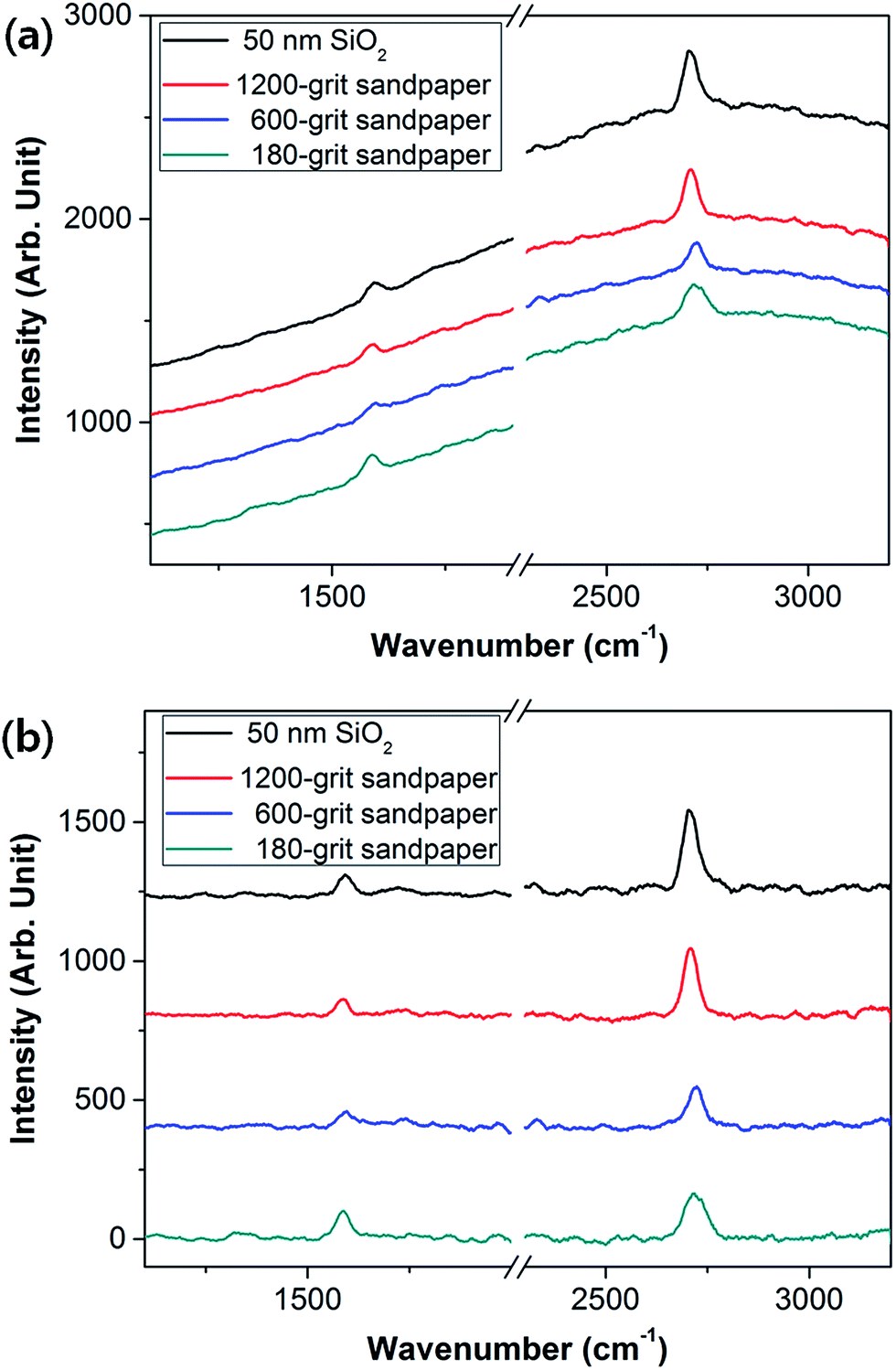
To characterize the graphenes grown on differently polished Cu films after annealing, Raman spectroscopic analysis was performed using the laser excitation of 514 nm, as shown in Fig. 4(a). Although the Raman spectra show high background signals due to the surface plasmon emission of Cu with a maximum around 600 nm,21 the main G- and 2D-peaks of graphene are clearly observed at around 1588 and 2707 cm−1, respectively. To elucidate the variation of the Raman spectra depending on different mechanical polishing conditions, we applied a background subtraction and normalization procedure on the measured Raman spectra for graphenes grown on the Cu foils, as shown in Fig. 4(b). Then, the spectra show typical profiles of monolayer graphene: the 2D band has a Lorentzian lineshape with a peak intensity ratio of the 2D band to the G band (I2D/IG) greater than 1.22 Here, it is noted that the I2D/IG increases from 1.7 for 180-grit sandpaper polishing to 3.4 for 50 nm SiO2 polishing, while the FWHM of 2D-band decreases from ∼50 to ∼30 cm−1 for each case. This result indicates that the quality of CVD-graphene is significantly improved by the annealing and mechanical polishing process.
 | ||
| Fig. 4 (a) Raman spectra of the graphenes grown on the differently polished Cu films after annealing and (b) corresponding Raman spectra after a background subtraction and normalisation. The peak intensity ratio of 2D/G increases and the FWHM of 2D band decreases as the grain size of the annealed Cu film underneath the graphene increases by mechanical polishing with 180-, 600-, and 1200-grit sandpapers and further with 50 nm SiO2. | ||
Since the grain size of the Cu film continuously increases and the surface roughness decreases by annealing and mechanical polishing with 180-, 600-, and 1200-grit sandpapers and further with 50 nm SiO2 particles, the electrical transport property of the graphene should be affected by the surface morphology of the underlying Cu films. Thus, the sheet resistance of graphene was measured using a Keithley-2700 multimeter with the van der Pauw method. Indium is attached on the four corners of a square to make ohmic contact with four electrodes. The van der Pauw method involves applying a current and measuring voltage using four small contacts on the circumference of a flat uniform thickness. This method does not depend on the sample size. The sheet resistance, Rs, of a thin film is given by,
 | (2) |
 | (3) |
Fig. 5 shows the sheet resistance of graphene in terms of surface roughness of the raw and annealed Cu films. It is expected that the grain size of graphene is proportional to the size of the Cu grain and its surface roughness increases with that of Cu. The surface roughness of Cu film corresponds to ∼10 nm for 50 nm SiO2, to ∼100 nm for 1200-grit sandpaper, ∼1 μm for 600-grit sandpaper and ∼10 μm for 180-grit sandpaper, respectively. The sheet resistance of graphene processed by mechanical polishing for raw Cu decreases with 57% from 1042 to 453 ohm sq−1 and that of graphene for annealed Cu decreases with 45% from 657 to 362 ohm sq−1. Thus, the sheet resistance of graphene decreases as the surface roughness of Cu film decreases. The sheet resistance of graphene for 50 nm SiO2 polishing shows a 20% decrease by the annealing process. It is also noted that the sheet resistance of graphene decreases as the size of Cu grain increases from 10 μm to 300 μm. Therefore, our research quantitatively demonstrates the effect of grain size and surface roughness of a Cu film on the sheet resistance of graphene using an annealing process and a mechanical polishing technique.
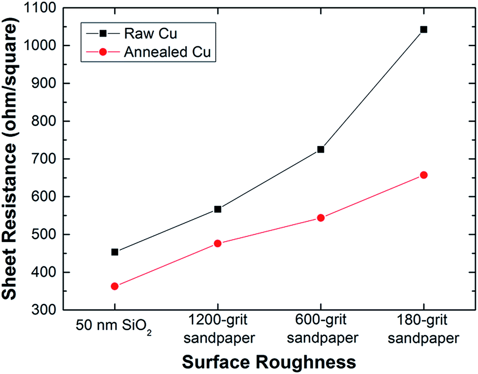 | ||
| Fig. 5 Sheet resistance of graphene vs. Cu surface roughness, showing a decrease in sheet resistance as the surface roughness of copper film is reduced. The sheet resistance of graphene grown on the annealed Cu film is lower due to a larger grain size, compared to that of graphene grown on the raw Cu film. | ||
Conclusions
We have shown that the sheet resistance of graphene grown on Cu substrate decreases as the surface roughness of the Cu film is reduced, and the grain size of the Cu film increases. The grain size of the Cu substrate is increased from 10 to 300 μm by annealing Cu film for 2 hours at 1060 °C. The different surface roughness of Cu film is prepared by a mechanical polishing method with different grit number of sandpapers, as well as 50 nm SiO2 particles. The surface roughness of the raw and annealed Cu film is reduced to 17 nm by mechanical polishing with the SiO2 nanoparticles. This research suggests that high quality CVD-graphene can be grown on a Cu film by applying annealing and mechanical polishing processes.Acknowledgements
This work was supported by the Rare Isotope Science Project of Institute for Basic Science funded by the Ministry of Science, ICT and Future Planning (MSIP) and the National Research Foundation (NRF) of the republic of Korea under contract 2013M7A1A1075764.Notes and references
- A. K. Geim, Science, 2009, 324, 1530 CrossRef CAS PubMed.
- F. Schwierz, Nat. Nanotechnol., 2010, 5, 487 CrossRef CAS PubMed.
- Y. Wu, Y. Lin, A. A. Bol, K. A. Jenkins, F. Xia, D. B. Farmer, Y. Zhu and P. Avouris, Nature, 2011, 472, 74 CrossRef CAS PubMed.
- J.-K. Lee, S. Yamazaki, H. Yun, J. Park, G. P. Kennedy, G.-T. Kim, O. Pietzsch, R. Wiesendanger, S. Lee, S. Hong, U. Dettlaff-Weglikowska and S. Roth, Nano Lett., 2013, 12, 3494 CrossRef PubMed.
- F. Bonaccorso, Z. Sun, T. Hasan and A. C. Ferrari, Nat. Photonics, 2010, 4, 611 CrossRef CAS.
- Y. Sun, Q. Wu and G. Shi, Energy Environ. Sci., 2011, 4, 1113 CAS.
- J. Shen, Y. Zhu, X. Yang and C. Li, Chem. Commun., 2012, 48, 3686 RSC.
- X. Li, W. Cai, J. An, S. Kim, J. Nah, D. Yang, R. Piner, A. Velamakanni, I. Jung, E. Tutuc, S. K. Banerjee, L. Colombo and R. S. Ruoff, Science, 2009, 324, 1312 CrossRef CAS PubMed.
- S. Kumar, N. McEvoy, T. Lutz, G. P. Keeley, V. Nicolosi, C. P. Murray, W. J. Blau and G. S. Duesberg, Chem. Commun., 2010, 46, 1422 RSC.
- Y. Pan, H. Zhang, D. Shi, J. Sun, S. Du, F. Liu and H. Gao, Adv. Mater., 2009, 21, 2777 CrossRef CAS.
- J. Coraux, A. T. N'Diaye, C. Busse and T. Michely, Nano Lett., 2008, 8, 565 CrossRef CAS PubMed.
- S. Bae, H. Kim, Y. Lee, X. Xu, J.-S. Park, Y. Zheng, J. Balakrishnan, T. Lei, H. R. Kim, Y. I. Song, Y.-J. Kim, K. S. Kim, B. Ozyilmaz, J.-H. Ahn, B. H. Hong and S. Iijima, Nat. Nanotechnol., 2010, 5, 574 CrossRef CAS PubMed.
- X. Li, C. W. Magnuson, A. Venugopal, R. M. Tromp, J. B. Hannon, E. M. Vogal, L. Colombo and R. S. Ruoff, J. Am. Chem. Soc., 2011, 133, 2816 CrossRef CAS PubMed.
- I. Vlassiouk, S. Smirnov, I. Ivanov, P. F. Fulavio, S. Dai, H. Meyer, M. Chi, D. Hensley, P. Datskos and N. V. Lavrik, Nanotechnology, 2011, 22, 275716 CrossRef PubMed.
- Z. Jin, T. P. McNicholas, C.-J. Shih, Q. H. Wang, G. L. C. Paulus, A. J. Hilmer, S. Shimizu and M. S. Strano, Chem. Mater., 2011, 23, 3362 CrossRef CAS.
- G. A. Lopez and E. J. Mittemeijer, Scr. Mater., 2004, 51, 1 CrossRef CAS PubMed.
- Y. Zhang, L. Zhang, P. Kim, M. Ge, Z. Li and C. Zhou, Nano Lett., 2012, 12, 2810 CrossRef CAS PubMed.
- Z. Yan, J. Lin, Z. Peng, Z. Sun, Y. Zhu, L. Li, C. Xiang, E. L. Samuel, C. Kittrell and J. M. Tour, ACS Nano, 2012, 6, 9110 CrossRef CAS PubMed.
- H. S. Song, S. L. Li, H. Miyazaki, S. Sato, K. Hayashi, A. Yamada, N. Yokoyama and K. Tsukagoshi, Sci. Rep., 2012, 2, 337 CAS.
- Z. Luo, Y. Lu, D. W. Singer, M. E. Berck, L. A. Somers, B. R. Goldsmith and A. T. Charlie Johnson, Chem. Mater., 2011, 23, 1441 CrossRef CAS.
- A. Mooradian, Phys. Rev. Lett., 1969, 22, 185 CrossRef CAS.
- A. C. Ferrari, J. C. Meyer, V. Scardaci, C. Casiraghi, M. Lazzeri, F. Mauri, S. Piscanec, D. Jiang, K. S. Novoselov, S. Roth and A. K. Geim, Phys. Rev. Lett., 2006, 97, 187401 CrossRef CAS.
- H. Kim, C. S. Park and H. D. Cho, Opt. Commun., 2014, 330, 131 CrossRef CAS PubMed.
- A. K. Kulkarni, K. H. Schulz, T. S. Lim and M. Khan, Thin Solid Films, 1999, 345, 273 CrossRef.
| This journal is © The Royal Society of Chemistry 2014 |