Pichaya Pattanasattayavonga,
Maria Sygletoub,
Emmanuel Kymakisc,
Emmanuel Stratakisb,
Feng Yand,
Vasilis G. Gregoriouef,
Thomas D. Anthopoulosa and
Christos L. Chochos*f
aDepartment of Physics and Centre for Plastic Electronics, Imperial College London, Exhibition Road, South Kensington, London SW7 2AZ, UK
bInstitute of Electronic Structure and Laser (IESL), Foundation for Research and Technology-Hellas (FORTH), Heraklion, 71110 Crete, Greece
cCentre of Materials Technology & Photonics and Electrical Engineering Department, Technological Educational Institute (TEI) of Crete, Heraklion, 71004 Crete, Greece
dDepartment of Applied Physics and Materials Research Centre, The Hong Kong Polytechnic University, Hong Kong, China
eNational Hellenic Research Foundation, 48 Vassileos Constantinou Avenue, Athens 11635, Greece
fAdvent Technologies SA, Patras Science Park, Stadiou Street, Patra, Platani-Rio, 26504, Greece. E-mail: cchochos@advent-energy.com
First published on 31st October 2014
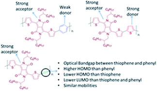
It is presented that the introduction of an alkyne linkage could be an important tool for fine-tuning the electronic and optoelectronic properties of certain donor–acceptor (D–A) conjugated polymers. Extensive optoelectronic studies in an alternating copolymer consisting of diketopyrrolopyrrole (DPP) and ethynylene linkage (TDPPTTB) and comparison over its fully cyclic DPP analogues, such as phenyl (TDPPTP) and thiophene (TDPPTT) rings reveals the role of the ethynylene moiety when it is introduced into the polymer backbone. The ethynylene moiety decreases the donor character of the thiophenes that flank the DPP therefore the highest occupied molecular orbital (HOMO) level of TDPPTTB is situated between the HOMO levels of the TDPPTP and TDPPTT. The optical band gap (Eoptg) of TDPPTTB is fixed between the Eoptg of TDPPTT and TDPPTP with a significant blue-shift in its absorption maximum. Furthermore, detailed studies on the electronic properties of TDPPTTB have been performed in Field Effect Transistors (FETs) using various dielectric materials. Transistors based on TDPPTTB films annealed at 120 °C show ambipolar behaviour, similar to TDPPTP and TDPPTT, with carrier mobilities of 0.03 cm2 V−1 s−1 for holes and 0.02 cm2 V−1 s−1 for electrons.
Modulation of molecular energy levels is one of the most important topics in molecular design of organic semiconducting materials. For many applications, such as OLEDs and photovoltaics, the value of the HOMO–LUMO gap is critical to an optimized device because it determines the colour of the emitted light in the LED or the effectiveness with which solar radiation is absorbed in photovoltaic devices.8 However, the control of the HOMO and LUMO energy levels is not a very simple process. Common tools that are employed to fine tune the band gap and energy level alignment of conjugated polymers are the donor–acceptor (D–A) approach and the quinoid structure.9 Despite the fact that the D–A approach is commonly used for the synthesis of a plethora of new low band gap (LBG) conjugated polymers, many issues remain to be addressed for understanding how their optoelectronic properties are fine-tuned, including the relative strength, the placement, and the ratio of the donor and acceptor moieties in the polymer backbone.5
Diketopyrrolopyrrole (DPP) based polymers are currently displaying some of the highest mobilities in field effect transistors (FETs) and PCE in OPVs.10 The potential of DPP-containing polymers as semiconductor materials for OFETs was presented in 2005.11 Two of the most extensively studied DPP-based copolymers consisting of either a thiophene12 or phenyl13 ring next to the thiophene–diketopyrrolopyrrole–thiophene (TDPPT) segment are presented in Scheme 1. TDPPTT and TDPPTP copolymers exhibit remarkably high hole mobilities up to 0.3 cm2 V−1 s−1 and PCEs above 7.0%.14,15 Very recently, Janssen et al. presented the synthesis of regular alternating DPP-based terpolymers containing both thiophene and phenyl rings in the polymer backbone, in an attempt to optimize their optoelectronic properties.16 Other co-monomers that have also been used are bithiophene,17 thieno[3,2-b]thiophene,18 furan,19 selenophene,20 naphthalene,21 vinylene,22 benzodithiophene23 and dithienothiophene24 (Scheme 1).
In this work, ethynylene bond is proposed and extensively explored as another chemical building block to modify the optoelectronic properties in DPP-based copolymers. The synthesis of an alternating copolymer comprising of the TDPPT segment and ethynylene unit (TDPPTTB; Scheme 1) is presented. Moreover, a direct comparison between the high performance TDPPTT and TDPPTP copolymers and the newly synthesized TDPPTTB will be performed in order to understand the relative strength (weak, intermediate, strong) of the ethynylene bond as compared to the thiophene and phenyl rings and how this affects the optoelectronic properties of DPP copolymers.
![]() | ||
Fig. 1 The results of the dihedral angles as calculated from the model compounds consisting of TDPPT unit and phenyl, thiophene and ethynylene groups. |
TDPPTTB was synthesized by Stille aromatic cross-coupling polymerization25 using tetrakis(triphenylphosphine)-palladium (0) [Pd(PPh3)4] as the catalyst in toluene solution between the 3,6-bis(5-bromothiophen-2-yl)-2,5-bis(2-hexyldecyl)pyrrolo[3,4-c]pyrrole-1,4(2H,5H)-dione and the 1,2-bis(trimethylstannyl) ethyne (Scheme 2). The polymerization reaction was performed at 110 °C under argon atmosphere for 12 h. After purification using Soxhlet extraction, the chloroform-soluble fraction of the TDPPTTB exhibits molecular weight of Mn = 20000 g mol−1 (PDI = 2.0) as measured by gel permeation chromatography (GPC) on monodisperse polystyrene standards utilizing chloroform as the eluent. The polymer exhibits very good solubility in chlorinated solvents.
Passing from solution to the solid state the absorption spectrum of TDPPTTB becomes broader and the λmax is 5 nm red shifted as compared to λmax in solution with the appearance of a pronounced shoulder at around 800 nm. The red shift of 5 nm in λmax of TDPPTTB is significantly lower as compared to TDPPTT (23 nm) and TDPPTP (13 nm).12,13 The λonset of TDPPTTB is situated at 910 nm, corresponding to an optical band gap of 1.36 eV. The optical band gaps of TDPPTP and TDPPTT are 1.53 eV and 1.30 eV, respectively. Therefore, the ethynylene bond fine tunes the optical band gap of DPP-based copolymers between the optical band gaps deduced when phenyl or thiophene rings are used.
The emission spectrum of TDPPTTB has also been recorded in the solid state (Fig. 2). TDPPTTB exhibits photoluminescence in the near infrared (NIR) spectrum with an emission maximum at 878 nm and a pronounced shoulder at 933 nm. This implies that TDPPTTB, in mixtures with suitable electron acceptor materials, can be a suitable candidate for applications in NIR photodetectors. Further studies on the electroluminescence properties of TDPPTTB are underway.
The density functional theory calculations using the B3LYP/6-31G(d,p) performed on the tetramer model compounds of TDPPTB, TDPPTT, and TDPPTP (Fig. 3) provide an estimation of the HOMO, LUMO, and band gap energies. There is an excellent trend between the theoretical and experimental LUMO levels as well as on the electrochemical band gap with the theoretical prediction for the DPP-based copolymers. On the other hand, while the trend between the experimental and theoretical HOMO levels of TDPPTT and TDPPTP are in good agreement, there is a minor discrepancy on the HOMO level of TDPPTTB. The experimental HOMO level of TDPPTTB shows that it is situated between the HOMO levels of TDPPTT and TDPPTP while the calculation shows that the HOMO level is situated at deeper values as compared to TDPPTT and TDPPTP.
![]() | ||
Fig. 4 AFM measurements showing topography and phase images of TDPPTTB film annealed at different temperatures. The scan size is 1 μm by 1 μm. |
Transistors employing the TG-BC architecture based on TDPPPTTB and either of the two dielectrics, Cytop and P(VDF-TrFE-CFE), were next fabricated and measured [Fig. 6(a)]. The annealing condition was chosen to be 120 °C due to good performance and more balance hole and electron transport as seen from the results of BG-BC transistors. The representative transfer and output characteristics of Cytop-based devices are shown in Fig. 6(b). Ambipolar behaviour is also observed with electron transport dominating. Ion–off of electrons is 105 while that of holes is 2 × 10⁴. Mobilities of electrons are approximately 4–5 times larger than those of holes both in linear and saturation regimes. μlin of electrons and holes are 0.008 cm2 V−1 s−1 and 0.002 cm2 V−1 s−1, and μsat are 0.02 cm2 V−1 s−1 and 0.004 cm2 V−1 s−1, respectively. Dtr of both carriers are not drastically different however, i.e., 3.6 × 10¹² and 4.5 × 1012 cm2 V−1 s−1. We speculate that the difference between electron and hole transport is possibly due to deep trap states that are not assessable using Dtr which relies on the subthreshold characteristics of the transistors. Instead, these deep traps manifest themselves in the onset voltage. Indeed for these Cytop-based devices, Von of electrons is 50 V while that of holes is around −120 V, suggesting that there are more deep hole traps than deep electron traps. Low-voltage operation is achieved by employing the high-k relaxor ferroelectric polymer P(VDF-TrFE-CFE) as the dielectric layer.27 The geometric capacitance of P(VDF-TrFE-CFE) film used in this work was obtained from an impedance analysis measurement at 10 Hz and found to be 200 nF cm−2. Fig. 6(c) shows the representative transfer and output characteristics of low-voltage TDPPTTB transistors. The ambipolar behaviour in this case is slightly dominated by hole transport. Ion–off for both carriers are close to 103. Mobilities of holes are 3–4 times larger than those of electrons. μlin of electrons and holes are 0.0005 cm2 V−1 s−1 and 0.002 cm2 V−1 s−1, and μsat are 0.002 cm2 V−1 s−1 and 0.005 cm2 V−1 s−1, respectively. Again, the difference in the transport performance is not mirrored in the Dtr which are around 5.3–5.6 × 1013 cm−2 eV−1 for both carriers. Similar to the Cytop-based devices, the imbalance shows in Von which is 7 V for electrons and −1.5 V for holes.
Fig. 7 summarizes and compares the performance in terms of carrier mobility among different dielectrics of TDPPTTB-based transistors. The details of the density of states in the semiconductor and/or at the semiconductor/dielectric interface are needed to understand comprehensively about the difference in the performance; however, this is out of the scope of this work and will be a subject of further studies. The mobilities obtained here especially in the case of HMDS-treated SiO2 dielectric are comparable to values reported earlier for TDPPTP and TDPPTT transistors.12,13 The introduction of the ethynylene moiety therefore enables the tuning of the energy levels of TDPPT-based polymers without adversely affecting the charge transport properties, hence find possible applications in different optoelectronic devices, including OFETs, OPVs and NIR photodetectors.
![]() | ||
Fig. 7 Mobilities (μ) of TDPPTTB transistors based on different dielectrics. All values are calculated from 120 °C-annealed TDPPTTB films. |
The UV-Vis absorption spectra of TDPPTTB in chloroform solution (0.2% w/v) and as thin film were measured with a LAMBDA 950 UV/VIS/NIR Spectrophotometer of Perkin Elmer with spectral range from 250 nm to 2500 nm. For the preparation of the film, the solution was drop casted on quartz substrate. After the evaporation of the solvent, the film was ready for study. For the PL spectra a thin layer of TDPPTTB was spin-coated onto a quartz substrate and placed into a vacuum chamber with optical access. For sample excitation a He–Cd CW laser operating at a wavelength of 325 nm, with 35 mW power is used. The PL spectra were measured at room temperature and resolved by using a UV grating and a sensitive, calibrated liquid nitrogen cooled CCD camera.
Fourier transform infrared (FT-IR) spectrum was measured on a BRUKER FT-IR spectrometer IFS 66v/F (MIR). The sample was in a powder form. In addition, the polymer was characterized by Raman spectroscopy at room temperature on a Nicolet Almega XR Raman spectrometer with a 473 nm blue laser as an excitation source. For the preparation of the samples, the solution was deposited on Si wafers.
CV studies were performed using a standard three-electrode cell. Platinum disk electrode was used as working electrode, platinum mesh as the counter-electrode and platinum wire as a reference electrode. Tetrabutylammonium hexafluorophosphate (TBAPF6; 98%) was used as electrolyte and was recrystallized three times from acetone and was dried in a vacuum at 100 °C before each experiment. Measurements were recorded using an EG&G Princeton Applied Research potentiostat/galvanostat Model 2273A connected to a personal computer running PowerSuite software. In a typical experiment, 2–5 mg of the material was diluted in 0.1 M TBAPF6 solution in o-DCB at a potential scan rate of 100 mV s−1. The reduction potentials were calibrated against a ferrocene/ferrocenium (Fc/Fc+) redox couple.
All calculations of the model compounds studied in this work have been performed using the Gaussian 03 software package.28 The alkyl substituents have been replaced with methyl groups in the model compounds for our calculations. While the presence of these long alkyl chains enhances the solubility of these polymers and affect the charge carrier mobility and photovoltaic behaviour of the polymer,29–31 from a computational point of view their replacement with shorter chains does not affect their optoelectronic properties (HOMO, LUMO and band gap) and thus the optimized structures of the molecules.32 The ground-state geometry of each model compound has been determined by a full geometry optimization of its structural parameters using the density function theory (DFT) upon energy minimization of all possible isomers. In this work, the DFT calculations were performed using the Becke's three-parameter hybrid functional, B3, with non-local correlation of Lee–Yang–Parr, LYP, abbreviated as B3LYP in conjunction with the 6-31G(d,p) split valence polarized basis set. All calculations were performed in vacuum. No symmetry constraints were imposed during the optimization process. The geometry optimizations have been performed with a tight threshold that corresponds to root mean square (rms) residual forces smaller than 10−5 au for the optimal geometry. The energy level of the HOMO and the LUMO of the repetitive units of each polymer were carried out by using the same set of calculations. DFT/B3LYP/6-31G(d,p) has been found33 to be an accurate formalism for calculating the structural and electronic properties of many molecular systems. In our studies the theoretical calculations performed on the tetramer model compounds for DFT describe in good proximity the experimental band gaps, in a similar manner to recent studies in other molecular systems.34,35
Bottom-gate bottom-contact (BG-BC) transistors were fabricated using Si++/SiO2 (200 nm) substrate with ITO/Au (10 nm/30 nm) source/drain (S/D) electrodes pre-patterned with standard photolithography. The silicon substrate also served as a gate contact in this case. SiO2 dielectric was treated with hexamethyldisilazane (HMDS) using vapour deposition at 80 °C for 30 min followed by thermal annealing also at 80 °C for another 30 min. TDPPTTB was spin-cast at 2000 rpm for 60 s from a 10 mg mL−1 solution in o-DCB which was kept stirring at 100 °C during the deposition. The film was annealed at 100 °C for 15 min before electrical characterization. The effects of thermal annealing were studied by annealing the samples further at 120, 140, and 160 °C for 15 min each time, and electrical characterization was performed after each annealing. Top-gate bottom-contact (TG-BC) transistors were fabricated on glass substrates with Al/Au (5 nm/25 nm) S/D contacts prepared by thermal evaporation through a shadow mask. TDPPTTB was spin-cast using the same procedure as the BG-BC FETs preparation but annealed at 120 °C for 15 min. The dielectric layer was then spin-cast on top of the semiconductor followed by a 40 nm-thick Al gate electrode also thermally evaporated through a shadow mask. Two types of dielectrics were used in this work: (1) Cytop (Asahi Glass), spin-cast at 2000 rpm for 60 s and annealed at 100 °C for 30 min and (2) high-k relaxor ferroelectric poly(vinylidene fluoride-trifluoroethylene-chlorofluoroethylene) [P(VDF-TrFE-CFE) at 56/36.5/7.5 mol%] for low-voltage operation,27 spin-cast from a 30 mg mL−1 solution in 2-butanone at 3000 rpm for 30 s and annealed at 60 °C for 3 h. All transistor fabrication steps were carried out in dry nitrogen atmosphere. Current–voltage characteristics of the transistors were acquired with an Agilent B2902A source/measure unit. The analysis of the data was based on the gradual channel approximation. All measurements were performed in a dry nitrogen atmosphere. Films of TDPPTTB were prepared on glass substrates following the same procedure used to fabricate transistors. Samples were annealed at 100, 120, 140, and 160 °C each for 15 min. Topographic and phase images of TDPPTTB films were obtained using an Agilent 5500 atomic force microscope in tapping mode.
Footnote |
† Electronic supplementary information (ESI) available: 1H-NMR, FT-IR and Raman spectra, as well as the cyclic voltammograph of the synthesized polymer. Optimized co-ordinates of the monomer and tetramer model compounds after theoretical calculations. See DOI: 10.1039/c4ra11487f |
This journal is © The Royal Society of Chemistry 2014 |