TiO2 nanotubes with tunable morphologies

J. M. Hernández-López, A. Conde, J. J. de Damborenea and M. A. Arenas*
Centro Nacional de Investigaciones Metalúrgicas (CENIM-CSIC), Avda. Gregorio del Amo, 8, 28040 Madrid, Spain. E-mail: geles@cenim.csic.es

Received 29th September 2014 , Accepted 6th November 2014

First published on 12th November 2014


Abstract

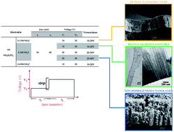
Titanium anodic oxide layers with a bottle shaped nanotubular structure have been grown in an electrolyte containing NH4F, applying voltage steps. The grown layers were analyzed using scanning and transmission electron microscopy (SEM and TEM), and Rutherford backscattering spectroscopy (RBS). The results show that a concentration of 0.15 M of NH4F in the anodizing bath, and a step of 10 to 20 V produces an oxide with a double morphology comprised of nanotubes at the oxide/metal interface and nanopores at the oxide/electrolyte interface of the anodic layer. Higher concentration of F in the bath, 0.3 and 0.45 M NH4F, enhanced the chemical dissolution of the anodic layer resulting in nanotubular structures along the oxide layer. Therefore, the bottle shaped nanotubular structures that show a well defined morphology are obtained in a bath containing a concentration of 0.3 M NH4F and applying a voltage step of 10–20 V.


1. Introduction

In recent years, the growth and/or deposition of titanium thin films and titanium oxide layers have received considerable attention in a variety of fields of endeavour such as: tissue engineering, drug delivery systems, orthopaedic implants, gas sensors, lithium ion batteries, solar cells, photovoltaic devices and have therefore encouraged its study and development.1–7 Different techniques such as laser, sputtering, sol–gel, thermal oxidation, electrophoresis and electroplating have been used to obtain TiO2 layers. Nevertheless, these techniques are limited when it comes to controlling the thickness of TiO2 and/or when dealing with the lack of uniformity in the grown layer.8,9

By contrast, the anodizing process allows the fabrication of uniform TiO2 layers with a controlled thickness and a variety of nanostructures that differs from barrier to porous layers, depending on the composition of the electrolyte used and the growth conditions (temperature, stirring, voltage and/or current applied).10,11 Zwilling et al. in 1999 obtained self-organized TiO2 nanoporous structures using diluted hydrofluoric acid solutions.12 Subsequent works showed that in these HF containing solutions, the thickness of TiO2 anodic layer was limited to 500–600 nm. The chemical dissolution resulting from the high acidity of the bath and the presence of fluorides,13 is responsible for this limitation in thickness. This drawback is overcome by the use of buffer solutions containing NaF or NH4F (where the chemical dissolution is decreased), along with pH control of the anodizing bath, leading to TiO2 layers up to 2 μm thick.14,15 It was precisely this increase in the thickness of the nanostructured TiO2 layers which made it possible to expand the niche of applications of TiO2 layers in those uses in which the nanostructure and thickness are critical, such as TiO2 fuel cells, which have improved their efficiency and service life by increasing the surface area.16,17

However, in addition to thickness, it is also possible to modify the diameter of the nanotubes by varying the applied voltage. Mor et al.,5 fabricated porous TiO2 layers with conical structures on titanium applying voltage ramps in an HF solution. The conical nanotubular layers had variable inner diameters throughout but the thickness of the oxide layer was limited to 200 nm. Similar nanostructures were obtained in organic electrolytes by applying ramps with ascending and descending voltages, leading to thicker anodic oxide layers and, therefore, greater surface areas of interest in the photocatalytic applications.18–22 Liu et al.23 fabricated TiO2 nanotubes with periodically changing morphology by using periodic pulses consisting of high and low voltages. However, the main drawbacks are either the instability of the organic baths, or the longer times required to achieve the desired thicknesses. In addition, most of the works are focused on pure titanium or titanium binary alloys and few papers are devoted to fabricate tailored nanotubes in the micrometer range on technologically relevant substrates such as Ti6Al4V alloy.

The objective of the present work is the growth of thick anodic layers in the micrometer range, with bottle shaped nanotubular structures in Ti6Al4V alloy in short times, less than two hours, and in aqueous anodizing baths that could be of interest for drug delivery control systems in orthopaedic prostheses. The work correlates the influence of the anodizing process parameters: the concentration of fluoride in the bath and the application of increasing voltage steps on the fabricated nanostructures.

2. Experimental procedure

Ti6Al4V alloy specimens of ELI grade according to the standard ASTM F136-02 supplied by SURGIVAL were ground using successive grades of SiC paper to 1200 grade, degreased with a detergent and rinsed in tap water followed by deionised water.

The specimens were then chemically polished in a mixture of HF(40 wt%)[thin space (1/6-em)]:[thin space (1/6-em)]HNO3(70 wt%)[thin space (1/6-em)]:[thin space (1/6-em)]H2O with a volume ratio of 1[thin space (1/6-em)]:[thin space (1/6-em)]4[thin space (1/6-em)]:[thin space (1/6-em)]5 for 5 min, at room temperature under continuous agitation at 400 rpm, rinsed in distilled water and dried in cold air. The working area was 2.54 cm2. Electrolytes containing 1 M NH4H2PO4 and 0.15, 0.3 and 0.45 M NH4F were prepared. Bottle shaped nanotubes were formed in a two-electrode cell. The specimens were anodized at stepped voltage with the first voltage (V1) applied for 30 min followed by a second voltage step (V2) applied for 60 min, as seen in Fig. 1. The temperature was controlled at 20 °C. Platinum mesh was used as a cathode. The voltages were applied using LAB/SM 1300 DC power supply (ET Power Systems Ltd). Current-time responses of anodizing were acquired at 0.1 Hz sampling rate using a zero-ohm ammeter connected in series with the electrochemical cell.


image file: c4ra11457d-f1.tif
Fig. 1 Fabrication conditions of nanotubes grown on Ti6Al4V.

The plan-view morphology of the nanotubular oxide films was examined by field emission gun scanning electron microscopy (FEG-SEM) utilizing JSM6500F Philips instrument equipped with EDX facilities and a ZEISS Ultra 55 scanning electron microscope. Electron-transparent sections were prepared by scratching the surface of the anodized specimens with a scalpel and collecting the pieces of the oxide on a TEM grid. TEM grids were observed using a JEOL JEM 2010 instrument operated at 200 keV.

The stoichiometric composition of the oxide films was further determined by Rutherford backscattering spectroscopy (RBS), using the following non-Rutherford elastic backscattering cross sections: He+ ions with the energy of 3.045 MeV (resonant energy for 16O(α,α0)16O reaction), 3.777 MeV (resonant energy for 19F(α,α0)19F reaction) and 5.725 MeV (resonant energy for 27Al(α,α0)27Al reaction) were produced by the van de Graff accelerator located at the Centro de Micro-Análisis de Materiales (CMAM), Madrid. The incident ion beam was normal to the surface of the specimen with 10 μC dose scattered ions detected by a mobile detector at 165°. Data were interpreted using the SIMNRA program.

3. Results and discussion

3.1. Current density versus time response

In the following sections, the current transients recorded during anodizing process were evaluated to determine the influence of the composition of the anodizing bath and voltage steps applied, i.e. electric field, on the anodic layers grown.
3.1.1. Influence of the composition of the anodizing bath. The current density versus time curves collected during the anodizing of Ti and its alloys, show significant growth aspects of the anodic oxide layer and its morphology.8,18,21,24 Fig. 2 shows the evolution of the current density versus time during the anodizing of the Ti6Al4V alloy in a 1 M NH4H2PO4 bath with different concentrations of NH4F applying voltage steps. In this figure, it is observed that the current-time transient, recorded for the different concentrations of NH4F used, is similar to that described by other authors for the anodizing of Ti and its alloys in aqueous media.5,8 Three different stages are distinguished: the growth of the high resistance oxide barrier layer – stage I; pores nucleation – stage II; and the steady state (growth of nanotubes)-stage III.
image file: c4ra11457d-f2.tif
Fig. 2 Current density–time responses of anodizing of Ti6Al4V at 10 V for 30 minutes followed by second voltage step at 20 V for 60 minutes (a), i vs. t response related to V1 = 10 V for 30 minutes (b) and V2 = 20 V for 60 minutes (c).

In this electrolyte, the pore initiation stage can be attributed to both the field-assisted ejection of Ti4+ ions into the electrolyte and the chemical dissolution of the oxide due to the presence of fluoride ions readily forming cavities within the oxide.

The three stages plotted in the current density versus time response are observed for each applied step voltage, V1 = 10 V for 30 minutes and V2 = 20 V for 60 minutes, Fig. 2b and c. The steady state current density recorded on stage III corresponding to the first applied voltage, V1 = 10 V, is 0.2 mA cm−2 for the bath containing 0.15 M NH4F and increases to 1.5 mA cm−2 for 0.45 M NH4F, Fig. 2b. The steady current density recorded for the second voltage step, V2 = 20 V, increases approximately 0.2 mA cm−2 compared to the values showed for the first voltage step for all the NH4F concentrations studied, Fig. 2c.

The increase in steady current density depending on the fluoride concentration in the bath indicates a greater chemical dissolution of the anodic layers with the fluoride content in the electrolyte.

The value of the final voltage (V2) determines the features of the anodic oxide layer grown on the oxide/metal interface.18–21,25 Therefore, the charge density related to the thickness of the barrier layer is calculated by integrating the stage I from the current density vs. time response corresponding to the second voltage step. These values vary between 33–83 mC cm−2 depending on the fluoride concentration in the bath, Table 1. Assuming that all the charge are only employed to form a dense layer of amorphous TiO2,21 the thickness of barrier layer varies from 18 to 45 nm, Table 1.

Table 1 Parameters of nanotubes formed in 1 M NH4H2PO4/[X] M NH4F
[X] M NH4F Step (30–60 min) Barrier film charge mC cm−2 Expected barrier oxide thickness, nma Charge C cm−2 Expected oxide thickness, nma NT inner diameter mouthb/bottomc, nm Barrier layer thicknessc, nm Total thicknessb, nm
a Calculate for compact amorphous film assuming 100% current efficiency.b Measured by SEM.c Measured by TEM.
0.15 10–20 V 33 18 1.393 758 ∼15/53 41 ∼661
0.3 69 38 4.807 2615 ∼47/69 39 ∼1355
0.45 83 45 9.322 5071 ∼63/65 40 ∼1585


Similarly, by calculating the total charge density used in the anodizing process, it can be seen that the total charge density increases with the fluoride content in the bath, from 1.393 to 9.322 mC cm−2 (Table 1). Assuming an efficiency of 100% for the titanium anodizing process, the thickness of the anodic layer would be 758 nm for a concentration of 0.15 M NH4F, 2615 nm for 0.3 M NH4F, and 5071 nm for 0.45 M NH4F, Table 1. However, as expected, the thickness values of the TiO2 layers measured by SEM differ significantly from the theoretical values calculated, Table 1, as it will be discussed later. This difference is increased with the fluoride content in the bath due to the higher chemical dissolution of the anodic layer which occurs in presence of fluorides since the dissolution rate of the oxide layer increases considerably with the F content.26

3.1.2. Influence of the electric field. To study the influence of the electric field on the nanostructure of the anodic layers, the magnitude of the voltage steps was varied for a specific concentration of fluorides, 0.3 M NH4F.

Fig. 3 shows the anodizing curves obtained for 0.3 M NH4F solution using different voltage steps. The evolution of the i vs. t curves is similar to those described in Fig. 2. Thus, after applying a voltage step of 10 V, an abrupt decrease in the current density related to the formation of the oxide barrier layer is observed, followed by the nucleation of the pores which does not exceed 300 seconds. Finally, the current density is maintained constant indicating that the steady state, in which the growth of the nanotubes takes place, has been reached (Fig. 3).


image file: c4ra11457d-f3.tif
Fig. 3 Current density–time responses of anodizing of Ti6Al4V in 1 M NH4FH2PO4/0.3 M NH4F at different voltage steps (a), with V1 = 10 V (b), with V1 = 20 V (c).

Upon applying the second voltage step, either 20 or 30 V, the current density at the steady state depicts higher oscillations than during the first voltage step of 10 V. This is due to the increase of the field-assisted dissolution of the anodic layer at voltages higher than 10 V, unbalancing the formation and dissolution of the anodic oxide layer.

The current density evolution at the steady state for a given ΔV = V2V1, indicates that the current density depends primarily on the applied ΔV rather than on the absolute values of each step, V1 and V2, see Fig. 3b and c.

Nevertheless, in the last 30 minutes of the 20–40 V treatment, the current density increases continuously, without actually reaching any steady state, thus revealing a greater field-assisted dissolution of the anodic layer at high voltages.

The results suggest that the main process occurring at stage III (constant nanotubular layer thickness over time) is field-assisted dissolution instead of “flow assisted” due to the significant level of dissolution of the oxide layer in this aqueous media.

3.2. Film morphology

In this section, the film morphology of the anodic layers fabricated using different anodizing conditions were characterized using scanning electron microscopy and transmission electron microscopy.

The morphology of the nanotubular layers fabricated in Ti6Al4V alloy by applying 10–20 V voltage steps in baths containing different NH4F concentrations is shown in Fig. 4. In all cases the formation of nanotubes preferentially grown in the α-phase, enriched in aluminium, along with the dissolution of the oxides in β-phase is observed. Such morphology has been widely described for F containing aqueous electrolytes. The absence of porous structures in the β-phase relates to the high solubility of vanadium oxides formed on this phase.5,8,12,15,27,28


image file: c4ra11457d-f4.tif
Fig. 4 Scanning electron micrographs. Morphology of the anodic layers grown at V1 = 10 V for 30 minutes and V2 = 20 V for 60 minutes on Ti6Al4V using (a) 0.15 M, (b) 0.3 M and (c) 0.45 M NH4F.

The micrographs gathered in Fig. 4 show the influence of the NH4F concentration in the nanotube inner diameter in the mouth, which varies from 15–63 nm for 0.15 M and 0.45 M NH4F, respectively, Table 1. This increase in the inner diameter of the nanotube is a result of the chemical dissolution of the nanotube walls due to the presence of fluorides in the electrolyte,27,29 according to the following reaction:

 
TiO2 + 6F + 4H+ → TiF2−6 + 2H2O (1)

This reaction may be further enhanced by the weakness of the bond between adjacent Ti and O due to the electric field (field-assisted dissolution).

Additionally in Fig. 4b and c it can be observed that in some areas the mouths of nanotubes appear to be plugged by a white oxide. This oxide is the result of the solubilization of the titanium and precipitation in form of hydrated species (TiO(OH)2 or Ti(OH)4).24,28,30,31

The thickness of the grown layers measured by SEM varies from 661 nm for the anodic layer fabricated in the bath with the lowest concentration of fluoride, up to 1585 nm approximately, for the layer obtained in a bath with the highest concentration, 0.45 M NH4F, Table 1.

Fig. 5a–f show the cross section of the anodic layers. Nanotubular structure can be distinguished in α-phase, while cavities caused by the preferential dissolution of the oxide formed in β-phase are observed.


image file: c4ra11457d-f5.tif
Fig. 5 Cross sections of anodic layers fabricated at 10–20 V in 1 M NH4H2PO4 with (a and b) 0.15 M, (c and d) 0.3 M and (e and f) 0.45 M of NH4F.

It is important to highlight that the lowest concentration of fluoride, 0.15 M NH4F, promotes a layer with double nanoporous-nanotubular structure, Fig. 5a–b. This complex morphology comprises an outer nanoporous part (∼180 nm thick) and inner nanotubular part. In the literature this bi-layered structure has been reported on pure titanium32 but also on Ti6Al4V.27 The explanation about the mechanism for the transition from nanoporous to nanotubular structure is unclear. According to Crawford et al.,32 the nanotubes grow deeper into the alloy due to the competition of oxide growth and chemical dissolution at the bottom of the nanotube. As nanotubes continue to grow, the nanoporous layer is subjected to chemical dissolution, resulting in thinning and eventual disappearance.

Conversely, the layers grown in baths with 0.3 M and 0.45 M NH4F have just a nanotubular structure throughout the thickness, Fig. 5c–f. The nanoporous layer disappears at higher concentration of fluorides in the bath, 0.3 and 0.45 M, since the nanoporous layer is subjected to a most intense chemical dissolution due to the higher fluorides presence in the bath.

The thickness of the barrier layer at the bottom of the nanotubes is about 40 nm, Table 1, suggesting an oxide growth rate of 2 nm V−1 within 60 min of anodizing.

The images of the cross-section of the anodic layers obtained by TEM clearly show the change in the nanotube inner diameter from the bottom to the mouth with the applied voltage step, Fig. 5d and f. Table 1, shows the inner diameters of the mouth and of the bottom of the nanotubes grown applying the stepped voltage, 10–20 V for the three anodizing baths. It can be seen that the best defined bottle shaped nanotubular structures are obtained for the bath containing 0.3 M NH4F. The design of bottle-shaped nanotubes with thicknesses greater than micrometer, is specially interesting for controlled drug delivery systems in orthopaedic prostheses.33

In addition, by applying different voltage steps, in a bath containing 0.3 M NH4F promotes changes in the nanotubular structures with regard to those previously described, Fig. 6a–h. The anodizing process performed at 10–30 V, Fig. 6c–d, shows poorly defined pores throughout the surface area, while the layers grown at 20–30 V Fig. 6e, show better defined nanotubular structures, similar to those obtained at 10–20 V, Fig. 6a. In the 20–40 V treatment, Fig. 6g, the formation of the nanotubes is not homogeneous over the entire surface, showing that the film looses integrity and collapses.


image file: c4ra11457d-f6.tif
Fig. 6 Scanning electron micrographs. Morphology of the anodic layers grown in 1 M NH4H2PO4 + 0.3 M NH4F at (a and b) 10–20 V, (c and d) 10–30 V, (e and f) 20–30 V, (g and h) 20–40 V.

Values of the inner diameter in the mouth and in the bottom of the nanotubes are included in Table 2.

Table 2 Parameters of nanotubes formed at different voltage steps
Electrolyte Step Charge (C cm−2) Expected oxide thicknessa, nm NT inner diameter mouth/bottom, nm Total thicknessb, nm Name
V1 30 min V2 60 min
a Calculate for compact amorphous film assuming 100% current efficiency.b Measured by SEM.c Measured at half of the oxide.
1 M NH4H2PO4 + 0.3 M NH4F 10 V 20 V 4.807 2615 ∼47/69 ∼1355 10–20 V
10 V 30 V 4.946 2690 ∼39/57c ∼1383 10–30 V
20 V 30 V 4.999 2720 ∼67/90 ∼1450 20–30 V
20 V 40 V 5.207 2839 ∼63/90c ∼1187 20–40 V


Nanotubes inner diameter depends primarily on the applied voltage since the voltage determines the electric field strength across the oxide, thus affecting the migration of ions and ultimately the nanotube inner diameter. The upper diameter (mouth diameter) is related to the value of the first applied voltage during the growth of the anodic layers. Layers which are grown with an initial voltage of 20 V (20–30 V and 20–40 V) have a larger pore diameter, in the range of 63–67 nm, compared to layers grown with an initial voltage of 10 V (10–20 V and 10–30 V) with diameters comprises between 39–47 nm, Table 2. Nanotubes bottom diameter depends on the second applied voltage. Values vary from 69 nm for 20 V to 90 nm for 40 V.

Assuming an efficiency of 100% for the titanium anodizing process, the thickness of the anodic layer fabricated using the different voltage steps applied ranges between 2600 and 2800 nm, Table 2. The thickness of the anodic layers measured by SEM are about 1400 nm for all anodic layers except for the layer grown at 20–40 V, which showed a smaller thickness, 1187 nm, Table 2. This difference can be attributed to the stronger electric field at 40 V compared to that obtained at lower applied voltages. This implies that there is a higher dissolution rate for the oxide being formed. This is clearly revealed in the anodizing curves, by the increasing current density recorded at stage III pointing out that a steady state is not reached, Fig. 3.

For the oxide layers fabricated, either in the solutions containing different fluoride concentrations, or varying the voltage steps, Fig. 5 and 6, the formation of ribs on the wall of the nanotubes is observed. Ribs have been widely described in the literature in aqueous electrolytes and organic electrolytes with a water content higher than 5%.18,34–36 Its formation occurs in a non-continuous way and is due to several factors such as the aggressiveness of the anodizing bath; mechanical stress generated during the growth of nanotubular oxide; the expansion factor; and the electric field generated by applying high voltage.

The inward migration of O2− ions during anodization fills the volume of metal consumed, but the outward migrating Ti4+ ions do not contribute to growth at the metal/oxide interface but pass directly into the solution. Fluoride ions migrate inward at twice the rate of oxygen ions across the layer and form a fluoride-rich layer at the metal/oxide interface. This fluoride-rich layer is more soluble in the anodizing electrolyte than the relatively pure TiO2 forming the majority of the layer thickness. The dissolution of the fluoride rich layer placed between the nanotubes walls (TiF4), according to reactions (2) and (3), increases the inter-space distance between the nanotubes. Therefore, the electrolyte accesses throughout the inter-space, and promotes the growth of a new barrier layer between the walls of adjacent nanotubes to form the ribs, in accordance with reaction (4):27,35,37

 
TiF4 + 2H2O → H+ + [TiF4(OH)H2O] (2)
 
[TiF4(OH)H2O] + HF → [TiF5·H2O] (3)
 
Ti + 2H2O → TiO2 + 4H+ + 4e (4)

Fig. 6h shows that the greater amplitude of the voltage step, i.e. 20–40 V, favours the formation of ribs along the nanotube to a greater extent than the other conditions studied. Moreover, in this case it appears that the inter-space distance is greater than at lower voltages thus indicating greater field-assisted dissolution of the nanotube walls at the highest applied voltages.

3.3. Efficiency of film formation and composition

In order to determine the composition of the anodic layers and estimate the efficiency of the anodizing process, the oxide layers were analysed by means of Rutherford Backscattering Spectroscopy (RBS).

Fig. 7a presents the RBS spectra corresponding to the anodic layers grown at voltage steps 10–20 V in electrolytes with different NH4F concentrations. All the spectra show a well-defined peak in channel 475 associated with oxygen, with the same number of counts, but with different width. The most significant difference among the spectra collected in Fig. 7a, is depicted in the slope plotted between channels 850 and 950 and is related to the presence of titanium in the anodic layer. As the concentration of fluoride in the electrolyte increases, the formation of a more pronounced step is observed. This step is related to the different thickness of the anodic layers, while the slope can be attributed to: differences in the roughness of the metal/oxide and oxide/surface interfaces; porosity of the grown layer; and heterogeneity of the oxide formed.


image file: c4ra11457d-f7.tif
Fig. 7 Rutherford backscattering analysis spectra for anodic oxide films formed on Ti-6Al-4V in 1 M NH4FH2PO4 + [x] M NH4F electrolyte at 10 V for 30 min and 20 V for 60 min, acquired at 3.777 MeV (a) and fitting of the spectra for the film formed in 0.15 M NH4F (b) circles-original data, solid line-simulation.

RBS spectra show a similar trend in the thickness of the anodic layers in relation to that measured by SEM. The layer fabricated in 0.15 M NH4F has the lowest thickness, while those grown in 0.3 M and 0.45 M NH4F are thicker and similar between them.

In order to determine the composition and thickness of the oxides grown, the simulation of RBS spectra was conducted using the SIMRA software, Fig. 7b and 8b. In order to simulate these complex oxide layers, the fitting of the spectra was performed assuming various layers of varying composition and thicknesses. The results show good agreement between the fitted and experimental data, for all cases.


image file: c4ra11457d-f8.tif
Fig. 8 Rutherford backscattering analysis spectra for anodic oxide films formed on Ti-6Al-4V in 1 M NH4FH2PO4 + 0.3 M NH4F electrolyte at different voltage steps, acquired at 3.777 MeV (a), fitting of the spectra for the film formed at 10–30 V, (b) circles-original data, solid line-simulation.

The composition of the anodic layers in 1015 atoms per cm2 and at.% is gathered in Table 3. It can be observed that the chemical composition for the layers fabricated in solutions containing different NH4F concentrations are similar among them, showing 33 to 34 at.% for oxygen, 47 to 51 at.% for titanium, 4 to 7 at.% for aluminium, 3 at.% for vanadium and fluorine contents about 9–10 at.%, Table 3.

Table 3 Composition of the nanotubular films (×1015 atoms cm−2), and at.% of each element, formed on Ti6Al4V in 1 M NH4H2PO4 electrolyte containing different NH4F concentrations, applying a voltage step of 10 V for 30 minutes and 20 V for 60 minutes
Film NH4F Ti O F Al V Average molecular composition Efficiency (%)
(×1015 at cm−2/at.%)
0.15 M 743/33 1142/51 221/10 92/4 60/3 TiO1.24·0.080TiF4·0.067Al2O3·0.044V2O5 34.24
0.30 M 1760/34 2389/47 485/9 346/7 145/3 TiO0.92·0.074TiF4·0.106Al2O3·0.044V2O5 23.53
0.45 M 1802/33 2594/47 536/10 383/7 156/3 TiO0.98·0.080TiF4·0.115Al2O3·0.047V2O5 12.42


The composition of the layers was determined assuming the stoichiometric formation of V2O5, Al2O3 and TiF4. The average molecular composition of the nanotubes formed on Ti6Al4V alloys can be expressed as TiO1.24·0.080TiF4·0.067Al2O3·0.044V2O5 for the layer grown in 0.15 M NH4F while for the layers grown at 0.3 and 0.45 M NH4F, the titanium oxide is composed of TiO0.92 and TiO0.98, respectively, Table 3. Similar contents of TiF4, Al2O3 and V2O5 are found for layers fabricated with 0.3 M and 0.45 M NH4F.

RBS spectra for layers grown in an electrolyte with 0.3 M of NH4F and different voltage steps, Fig. 8a, are similar to those obtained for the anodic layers grown with different concentrations of NH4F. A well-defined oxygen peak of similar width is observed in all growth conditions. There are no great differences in thickness between the layers. The anodic oxide layer fabricated at 20–30 V is slightly thicker, while the layer grown at 20–40 V, has the lowest thickness. These results are in agreement with those measured in the SEM images as is summarised in Table 2.

The composition of the titanium oxide layers is similar in all cases, showing 33 to 36 at.% for oxygen, 45 to 47 at.% for titanium, 7 at.% for aluminium, 2 to 3 at.% for vanadium and fluorine contents about 9–12 at.%, Table 4. The layer grown at 20–30 V presents a slightly higher Ti/O ratio, showing an average molecular composition expressed as TiO0.98 0.094TiF4 0.111Al2O3 0.045V2O5, while the oxide grown at 20–40 V, revealing a lower ratio of Ti/O, is composed of TiO0.87·0.073TiF4·0.098Al2O3·0.039V2O5, Table 4.

Table 4 Composition of the nanotubular films (×1015 atoms cm−2), and at.% of each element, formed on Ti6Al4V in 1 M NH4H2PO4 + 0.3 M NH4F, at different voltage steps
Film Ti O F Al V Average molecular composition Efficiency (%)
(×1015 at cm−2/at.%)
10–20 V 1760/34 2389/47 485/9 346/7 145/3 TiO0.92·0.074TiF4·0.106Al2O3·0.044V2O5 23.53
10–30 V 1842/34 2429/45 630/12 372/7 132/2 TiO0.93·0.093TiF4·0.109Al2O3·0.037V2O5 25.73
20–30 V 1938/33 2724/46 668/11 387/7 158/3 TiO0.98·0.094TiF4·0.111Al2O3·0.045V2O5 24.72
20–40 V 1674/36 2121/45 447/10 303/7 124/3 TiO0.87·0.073TiF4·0.098Al2O3·0.039V2O5 22.13


The efficiency of the anodizing process has been estimated using the expression that relates the concentration of titanium obtained from RBS spectra (concentration of Titanium in 1015 atoms per cm2, second column in Tables 3 and 4) and the calculated from the charge recorded during the anodizing (Tables 1 and 2), assuming that all the charge is consumed to oxidize titanium (100% efficiency):

 
image file: c4ra11457d-t1.tif(5)
where the Ti atoms per cm2 are estimated as follows:
 
Ti atoms per cm2 (current − time[thin space (1/6-em)]curves) = charge recorded × 1.5597 × 10¹⁸ at C−1 (6)
 
image file: c4ra11457d-t2.tif(7)
being 275 nm cm2 C−1 the titanium consumed by charge unit, ρ the titanium density, NA the Avogadro's number and WM the titanium molecular weight.

The results reveal an efficiency about 34.2% for the bath containing 0.15 M NH4F, and 12.4% for the bath with 0.45 M NH4F, Table 3. The efficiency decreases with the fluoride concentration in the bath despite the influence of the F content on the charge, as can be seen in the increasing current density response described in the curves in Fig. 2. This means that not all the collected charge is used to grow the titanium oxide, but that part of it is due to either the dissolution of both the nanotubes formed in the α phase and the oxidation of the β-phase, or to the oxygen evolution at the anode. The higher the fluoride concentration in the anodizing electrolyte, the lower the process efficiency. This response has been also described for TiO2 anodic layers fabricated in similar electrolytes at constant voltages.27,28

The efficiency of the anodizing process performed in the present work, applying voltage steps, Table 4, is 22–25%. It appears that efficiency of the anodizing process is not influenced by the voltages or by the ΔV applied. The results suggest that the growth efficiency depends mainly on the chemical dissolution of the oxide due to the fluoride presence in the electrolyte more than the field-assisted dissolution of the oxide and field-assisted ejection of Ti ions into the electrolyte.

4. Conclusions

In this paper it has been demonstrated that it is possible to design TiO2 oxide layers with bottle-shaped nanostructures by controlling the anodizing electrolyte and the applied voltage steps.

For the anodic layer fabricated applying voltage steps of 10–20 V, the F concentration mainly influenced the inner nanotubes diameter, which also depends on the value of the voltage applied. Electrolytes with low fluoride concentration, 0.15 M NH4F, lead to anodic layers with double morphology, nanoporous on the oxide/solution interface and nanotubular on the metal/oxide interface. Conversely, at higher fluoride concentrations, 0.3 M and 0.45 M NH4F, only a nanotubular oxide layer with variable inner diameter along the layer is fabricated. Therefore, the growth of bottle-shaped nanotubular oxide layers is achieved only when apply a voltage steps using the adequate fluoride concentration in the electrolyte. The best bottle-shaped morphology is obtained in the anodizing bath containing 0.3 M NH4F with a inner diameter about 47 nm at the mouth and about 69 nm at the bottom. This anodic layer is homogeneous and thicker than one micrometer.

Other voltage steps, 10–30 V, 20–30 V or 20–40 V, applied in the same anodizing bath-0.3 M NH4F – lead to oxide layers thicker than the micrometer but their nanostructures are not well defined.

Ribs on the wall of the nanotubes are observed for the oxide layers fabricated, either in the solutions containing different fluoride concentrations, or varying the voltage steps. Nevertheless, the formation of ribs are favoured for the greater amplitude of the voltage step, i.e. 20–40 V, than the other conditions studied. Additionally, the inter-space distance is also greater at 40 V than at lower voltages thus indicating greater field-assisted dissolution of the nanotube walls at the highest applied voltages.

The efficiency of the anodizing process decreases with the fluorides concentration in the bath, from 34.2% for 0.15 M NH4F, 22% for 0.3 M NH4F to 12.4% for 0.45 M NH4F, and is practically constant for the different voltages applied, about 22–25 %. It appears that efficiency of the anodizing process depends mainly on the chemical dissolution of the oxide due to the fluoride concentration in the electrolyte more than the field-assisted dissolution of the oxide and field-assisted ejection of Ti ions into the electrolyte.

Acknowledgements

The authors acknowledge to the Spanish Ministry of Science and Innovation-under Consolider-Ingenio 2010 CSD 2008-0023 FUNCOAT Project and to the Spanish Ministry of Economy and Competitiveness-under MUNSUTI Project – MAT2013-48224-C2-1-R-. Mr J. M.Hernández-López wishes to thank to CSIC for his PhD grant JAE-predoc.

References

  1. S. Minagar, C. C. Berndt, J. Wang, E. Ivanova and C. Wen, Acta Biomater., 2012, 8, 2875–2888 CrossRef CAS PubMed.
  2. M. Geetha, A. K. Singh, R. Asokamani and A. K. Gogia, Prog. Mater. Sci., 2009, 54, 397–425 CrossRef CAS PubMed.
  3. B. M. Holzapfel, J. C. Reichert, J. T. Schantz, U. Gbureck, L. Rackwitz, U. Noth, F. Jakob, M. Rudert, J. Groll and D. W. Hutmacher, Adv. Drug Delivery Rev., 2013, 65, 581–603 CrossRef CAS PubMed.
  4. L. Zhao, P. K. Chu, Y. Zhang and Z. Wu, J. Biomed. Mater. Res., Part B, 2009, 91, 470–480 CrossRef PubMed.
  5. G. K. Mor, O. K. Varghese, M. Paulose, K. Shankar and C. A. Grimes, Sol. Energy Mater. Sol. Cells, 2006, 90, 2011–2075 CrossRef CAS PubMed.
  6. E. Gultepe, D. Nagesha, S. Sridhar and M. Amiji, Adv. Drug Delivery Rev., 2010, 62, 305–315 CrossRef CAS PubMed.
  7. O. R. Brian and G. Michael, Nature, 1991, 353, 737–740 CrossRef.
  8. P. Roy, S. Berger and P. Schmuki, Angew. Chem., Int. Ed., 2011, 50, 2904–2939 CrossRef CAS PubMed.
  9. T. Goto, Int. Congr. Ser., 2005, 1284, 248–256 CrossRef CAS PubMed.
  10. Y.-T. Sul, C. B. Johansson, Y. Jeong and T. Albrektsson, Med. Eng. Phys., 2001, 23, 329–346 CrossRef CAS.
  11. G. Liu, K. Wang, N. Hoivik and H. Jakobsen, Sol. Energy Mater. Sol. Cells, 2012, 98, 24–38 CrossRef CAS PubMed.
  12. V. Zwilling, E. Darque-Ceretti, A. Boutry-Forveille, D. David, M. Y. Perrin and M. Aucouturier, Surf. Interface Anal., 1999, 27, 629–637 CrossRef CAS.
  13. C. A. Grimes and G. K. Mor, TiO2 Nanotube Arrays, Synthesis, Properties, and Applications, Springer, 2009, p. 358 Search PubMed.
  14. A. Ghicov, H. Tsuchiya, J. M. Macak and P. Schmuki, Electrochem. Commun., 2005, 7, 505–509 CrossRef CAS PubMed.
  15. J. M. Macak, H. Tsuchiya, L. Taveira, A. Ghicov and P. Schmuki, J. Biomed. Mater. Res., Part A, 2005, 75, 928–933 CrossRef PubMed.
  16. Y. Li, H. Yu, W. Song, G. Li, B. Yi and Z. Shao, Int. J. Hydrogen Energy, 2011, 36, 14374–14380 CrossRef CAS PubMed.
  17. J. Lin, J. Chen and X. Chen, Nanoscale Res. Lett., 2011, 6, 1–5 Search PubMed.
  18. D. Guan, P. J. Hymel and Y. Wang, Electrochim. Acta, 2012, 83, 420–429 CrossRef CAS PubMed.
  19. X. Wang, S. Zhang and L. Sun, Thin Solid Films, 2011, 519, 4694–4698 CrossRef CAS PubMed.
  20. X. Wang, R. Chen, J. Zheng, P. Nie, H. Xie and X. Zhao, J. Wuhan Univ. Technol., Mater. Sci. Ed., 2012, 27, 866–870 CrossRef CAS.
  21. D. Guan and Y. Wang, Nanoscale, 2012, 4, 2968–2977 RSC.
  22. D. Wang, Y. Liu, B. Yu, F. Zhou and W. Liu, Chem. Mater., 2009, 21, 1198–1206 CrossRef CAS.
  23. Y. Liu, D. Wang, L. Cao and S. Chen, Electrochem. Commun., 2012, 23, 68–71 CrossRef CAS PubMed.
  24. L. V. Taveira, J. M. Macák, H. Tsuchiya, L. F. P. Dick and P. Schmuki, J. Electrochem. Soc., 2005, 152, B405 CrossRef CAS PubMed.
  25. J. M. Macak, S. Albu, D. H. Kim, I. Paramasivam, S. Aldabergerova and P. Schmuki, Electrochem. Solid-State Lett., 2007, 10, K28–K31 CrossRef CAS PubMed.
  26. J. M. Macak, H. Hildebrand, U. Marten-Jahns and P. Schmuki, J. Electroanal. Chem., 2008, 621, 254–266 CrossRef CAS PubMed.
  27. E. Matykina, A. Conde, J. de Damborenea, D. M. y. Marero and M. A. Arenas, Electrochim. Acta, 2011, 56, 9209–9218 CrossRef CAS PubMed.
  28. E. Matykina, J. M. Hernandez-López, A. Conde, C. Domingo, J. J. de Damborenea and M. A. Arenas, Electrochim. Acta, 2011, 56, 2221–2229 CrossRef CAS PubMed.
  29. K. Yasuda and P. Schmuki, Electrochim. Acta, 2007, 52, 4053–4061 CrossRef CAS PubMed.
  30. J. M. Macak, H. Tsuchiya, A. Ghicov, K. Yasuda, R. Hahn, S. Bauer and P. Schmuki, Curr. Opin. Solid State Mater. Sci., 2007, 11, 3–18 CrossRef CAS PubMed.
  31. K. Yasuda, J. M. Macak, S. Berger, A. Ghicov and P. Schmuki, J. Electrochem. Soc., 2007, 154, C472–C478 CrossRef CAS PubMed.
  32. G. A. Crawford and N. Chawla, Acta Mater., 2009, 57, 854–867 CrossRef CAS PubMed.
  33. J. M. Hernández López, M. A. Arenas, A. L. Doadrio, A. Conde, C. Pérez-Jorge, J. J. de Damborenea, M. Vallet-Regi, E. Gómez-Barrena and J. Esteban. Proceedings of the 22nd Annual Meeting of the European Orthophaedic Research Sociaty, Nantes, France, 2014 Search PubMed.
  34. Y. A. Buslaev and V. A. Shcherbakov, J. Struct. Chem., 1966, 7, 332–336 CrossRef.
  35. A. Valota, D. J. LeClere, P. Skeldon, M. Curioni, T. Hashimoto, S. Berger, J. Kunze, P. Schmuki and G. E. Thompson, Electrochim. Acta, 2009, 54, 4321–4327 CrossRef CAS PubMed.
  36. J. M. Macak, H. Tsuchiya, L. Taveira, S. Aldabergerova and P. Schmuki, Angew. Chem., Int. Ed., 2005, 44, 7463–7465 CrossRef CAS PubMed.
  37. C. Lin, S. Chen and L. Cao, Mater. Sci. Semicond. Process., 2013, 16, 154–159 CrossRef CAS PubMed.

This journal is © The Royal Society of Chemistry 2014
Click here to see how this site uses Cookies. View our privacy policy here.