DOI:
10.1039/C4RA10519B
(Paper)
RSC Adv., 2014,
4, 55452-55458
Tuning the band gap and optical properties of γ-Si3N4 with rare earth element Ce
Received
16th September 2014
, Accepted 25th September 2014
First published on 25th September 2014
Abstract
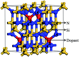
The present paper reports the investigation of optoelectronic properties of doped γ-Si3N4. The rare earth element Ce is used as a dopant. Two structures are picked out from the four ones with different doping methods by comparing their formation and binding energies. The effects of doping methods and concentrations are explored based on the favourable structures. Four cases with different concentrations are considered for each doping method. Their electronic and optical properties are calculated on the basis of hybrid density functional theory with Hubbard U correction. The Ce dopant with the proper doping method and concentration results in decreased band gaps, improved low-energy electron transition and enhanced absorption of solar energy. The mechanism for the doping effect is elucidated by analyzing the electronic structure.
1. Introduction
Silicon nitride (Si3N4) is an important engineering ceramic material owing to its superior mechanical properties, high chemical and thermal stability, and good wear resistance. It has been widely applied in cutting tools, engine components, ball bearings and gas turbines.1–3 α-Si3N4 and β-Si3N4 can be obtained using conventional synthesis conditions. Both phases are in the hexagonal crystal system. In 1999, the cubic spinel structure (γ-Si3N4) was synthesized by applying high pressure with high temperature.4 An ab initio density functional theory (DFT) calculation suggested that γ-Si3N4 has a direct band gap of 3.45 eV.5 This is in contrast to the band gaps of α- and β-Si3N4, whose band gaps are wider and indirect. The hardness of γ-Si3N4 can be compared to stishovite, and it is also increased in comparison to β-Si3N4. Because of the unique combination of mechanical and electronic properties, γ-Si3N4 is a candidate for optoelectronic applications, including UV LEDs and lasers.6 Studies have been carried out to examine the electric and optical properties of γ-Si3N4.7–9 However, further improvement of characteristics are necessary to allow these materials to become as widely used as their hexagonal predecessors. To be an efficient photoelectric material, γ-Si3N4 must have an optimal band gap and absorption coefficient of solar energy. However, the band gap of γ-Si3N4 is too wide and the optical absorption is too small to effectively convert solar energy. The doping method is used to improve the electronic and optical properties.10–12 Therefore, it is necessary to find an effective dopant and a relevant doping method to produce a new doped material. The material should have a reduced band gap and an enhanced absorption coefficient, but it should not have holes and intraband transitions. A rare earth element Ce (4f15d16s2) with vacant and weakly ionized d and f electrons is a possible effective dopant because it is relatively difficult to introduce holes, and also is used as a luminescence center.13–18 Recently, the luminescence properties of α-Si3N4 activated by Ce have been studied, and blue light emission was found.19 This study encouraged us to explore the optical properties of γ-Si3N4 caused by the Ce dopant. Here, we investigate a way to decrease the band gap and increase the adsorption of γ-Si3N4 with dopant Ce using the hybrid DFT and Hubbard U correction. Moreover, the doping method and concentration of dopant are emphasized. We also explored the mechanisms with electronic structure calculations to obtain a complete understanding of the doping effect.
2. Computational models and methods
Fig. 1 shows the modules of doped γ-Si3N4. It can be seen from the cubic spinel form that Si atoms occupy both tetrahedral (tet) and octahedral (oct) sites, but N atoms only occupy tet sites. When the Ce atom is doped, both substitutional and interstitial sites are possible doping sites, depending on the synthesis conditions. Ce@Si-T, Ce@Si-O and Ce@N are used for the doping method in which one Ce atom substitutes for a tet Si, oct Si and N atom, respectively. For the interstitial site of the Ce atom, the possible positions are enormous. Here we just list one of them (Ce-IN). The formation energy (Ef) that is calculated at the two extreme conditions, i.e., the Si-rich limit and the N-rich limit, is given as a function of the atomic chemical potentials and Fermi energy: Ef (q) = ET(q) − nSiμSi − nNμN − μx + qEF.1,2 The ET is the total energy of a supercell containing an impurity atom; nSi and nN represent the number of Si and N atoms, respectively; μSi, μN and μx are the chemical potentials of Si, N, and the impurity atoms, respectively; and EF is the Fermi energy. The binding energy (Eb) of the crystal, which is given as a function of total energy and the total sum of free energies, represents its energy stability.12 Therefore, the most suitable doping method of Ce dopant is suggested in terms of Ef and Eb, which are calculated using the model of the 56-atom supercell (2 × 2 × 2). Then, the influences of concentration on the electronic and optical properties are investigated based on the most suitable doping models. The doping concentration in this paper refers to atomic ratios. There are five equivalent tet Si atoms in the supercell, excluding the ones on the side of cell. When one Ce atom replaces one tet Si atom labeled as Ce@Si-T-I, the concentration is 0.042. The number of Ce atom is added to get higher doping concentrations of 0.083, 0.125, and 0.167, and the corresponding cases are labeled as Ce@Si-T-II, Ce@Si-T-III and Ce@Si-T-IV, respectively. To avoid the influence of interaction among multiple Ce atoms, the doped atoms are equally distributed in the models, and the distance between every two Ce atoms is about 5.6 Å. As for the Ce@Si-O cases, different concentrations are labeled Ce@Si-O-I, Ce@Si-O-II, Ce@Si-O-III and Ce@Si-O-IV. The calculations are conducted by a first-principles plane-wave pseudo-potential (PWP), using the CASTEP procedure of Materials Studio 6.0.20 The optimized structures are obtained via DFT calculations with the functional of GGA of PBE form. All the calculated electronic and optical properties are obtained with the use of the B3LYP hybrid functional. The norm-conserving pseudopotential is used in all the calculations of properties. The cutoff energy is chosen from the three tested values, which are 350, 400 and 450 eV. The energy level of 400 eV, which corresponds a 3 × 3 × 3 Monkhorst–Pack set of K-points, is effective to provide the convergent result. Different numbers of empty bands (20, 30, 40 and 50) are also tested in which the number of 40 is sufficient to achieve the correct band structure. Because of the existence of 4f-electrons, we considered the B3LYP + U method in the Ce doped cases. To achieve the accurate Hubbard U value of Ce-4f electrons, different values of U ranging from 6 to 16 eV are used. The Ce@Si-T-IV with good symmetry is set as the testing module. We chose the value of 10 eV, which can provide the maximal band gap value for the Ce-doped cases. The band gap value, depending on the U value, is shown in Fig. 2. Convergence criteria in energy, force, stress, and displacement are set as 2 × 10⁻⁵ eV, 0.05 eV Å−1, 0.1 GPa and 0.002 Å, respectively. The electronic structures and optical properties are calculated with the corresponding optimized crystal geometries. Optical properties of a material can be measured from the complex dielectric function, which consists of a real part ε1 and an imaginary part ε2; the real part can be calculated using Kramers–Krönig transformation. All other optical constants, such as the dielectric function, absorption coefficient and conductivity, are derived from ε1 and ε2, whereas the transmissivity is calculated with the method reported in ref. 21.
 |
| Fig. 1 Model of doped γ-Si3N4. | |
 |
| Fig. 2 The value of U versus band gap value. | |
3. Results and discussions
3.1. Calculated structure properties of doped γ-Si3N4
In terms of the Eb and Ef, we first find the most suitable doping method for the Ce dopant. If its Eb is negative, the doped cases are identified to be energy stable.12 The negative Ef with the higher absolute value indicates that the formation of the doped case is possible. Table 1 show that both Ce@Si-T and Ce@Si-O have negative Ebs and Efs. Moreover, the absolute value of Eb of Ce@Si-T is about 2.3 eV higher than that of Ce@Si-O, and the absolute value of Ef is also higher than those of Ce@Si-O in both the Si-rich and N-rich condition. This indicates that Ce@Si-T is more stable than Ce@Si-O and that the Ce atom is more inclined to occupy tet Si sites. Because of quite small absolute values of Eb and the positive values of Ef, Ce@N and Ce-IN methods are not suitable for doping; therefore, we omitted the analysis of these cases. By comparing the lattice parameter and average bond length with those of intrinsic γ-Si3N4, we find that doping Ce results in only a slight change. This indicates that Ce doping has not caused lattice distortion. Therefore, we concentrated on the methods of Ce@Si-T and Ce@Si-O to study the influence of doping concentration on the electronic and optical properties of doped γ-Si3N4.
Table 1 Calculated Efs, Ebs and structural properties for different doping structures. Ef_Si is calculated from the Si-rich limit while Ef_N from the N-rich limit
|
Ef_Si (eV) |
Ef_N (eV) |
Eb (eV) |
N–Si (avg) (Å) |
Lattice parameter (Å) |
Ref. 7. Ref. 9. |
γ-Si3N4 |
0.613 |
0.613 |
−455.034 |
1.862 |
7.771, 7.745a, 7.837b |
Ce@Si-T |
−3.103 |
−6.224 |
−453.398 |
1.875 |
7.871 |
Ce@Si-O |
−0.751 |
−3.872 |
−451.046 |
1.875 |
7.875 |
Ce@N |
29.095 |
31.435 |
−416.328 |
1.862 |
7.778 |
Ce-IN |
6.583 |
6.583 |
−449.065 |
1.895 |
7.926 |
3.2. Electronic properties of doped γ-Si3N4
3.2.1. Electronic properties of Ce@Si-T cases. Based on the analysis of Ef and Eb, we found that Ce@Si-T is a favorable doping method. However, the influence of Ce concentration on the electronic and optical properties of γ-Si3N4 should be considered. Fig. 3 shows the density of states (DOS) and band structure of intrinsic γ-Si3N4. The calculated direct band gap is 5.023 eV, which is in accordance with the recent experimental values 4.85 eV (ref. 5) and 4.8 eV,6 and better than other theoretical values, i.e. 3.45 eV,5 3.00 eV (ref. 10) and 3.58 eV,12 which are found in the literature. For intrinsic γ-Si3N4, the valence band (VB) originates mainly from N-2p orbitals, whereas the lowest conduction band is composed of Si orbitals. Fig. 4 shows the DOS and band structures of cases derived from Ce@Si-T with different doping concentrations. The shape of highest VB shows apparent change compared with intrinsic γ-Si3N4; moreover, the Ce-5d orbitals and Ce-4f orbitals add to the composition of the highest VB. For Ce@Si-T-I, the conduction band (CB) composed of the Si orbitals and few Ce orbitals decreases to 4.6 eV, which is reduced by 0.4 eV compared with the CB of intrinsic γ-Si3N4. Furthermore, a new occupied band composed of N-2p and Ce-5d orbitals appears, which is below the Fermi energy at around −0.2 eV. Because of the interaction among the electronic charges, which produces a multi-body effect or the overlap of impurities and defect band, the band gap narrows to 4.069 eV. With the increase in Ce concentration, the interaction among the electronic charges is enhanced. For Ce@Si-T-II, the location of the CB decreases by about 1.3 eV, which further narrows the band gap. With further increase in Ce concentration, the Burstein–Moss shift, which is a factor responsible for increasing the band gap, become evident and should not be neglected. As a result, the band gap of Ce@Si-T-III and Ce@Si-T-IV shows a slight increase of 3.122 eV and 2.973 eV, respectively. We can also observe from the band structure that γ-Si3N4 has a direct band gap with the highest VB and lowest CB located at the same point. Among the four Ce@Si-T cases, only the Ce@Si-T-III has the character of a direct band gap. With the reduced direct band gap, Ce@Si-T-III has potential for application in photodiodes.
 |
| Fig. 3 Density of states and band structure for intrinsic γ-Si3N4. | |
 |
| Fig. 4 Density of states and band structures for Ce@Si-T cases. | |
3.2.2. Electronic properties of Ce@Si-O cases. Considering that the doping methods of Ce@Si-O and Ce@Si-T have a similar Eb, the electronic structure of the high concentration cases derived from Ce@Si-O are calculated and compared with those derived from Ce@Si-T. For the same doping concentration, Ce@Si-O is more effective for decreasing the band gap of γ-Si3N4 (Fig. 5). Ce@Si-O-I has a direct band gap of 2.440 eV, whereas that of Ce@Si-T-I is 4.069 eV. The composition of VB and CB of Ce@Si-O-I is similar to that of Ce@Si-T-I. However, the distribution of the orbitals and the band gap values are different from those of Ce@Si-T-I. This is because the different doping method used for Ce (Ce@Si-T or Ce@Si-O) causes a different interaction of electronic charges, and thus the overlap of impurities and defect band show different effects. It should be noted that the band gap values of the Ce@Si-O cases decrease continuously with increase in doping concentration. This indicates that the multi-body effect plays a leading role in reducing the band gap value in the Ce@Si-O cases. When the Ce concentration reaches 0.16, the Ce-5d orbitals of Ce@Si-O-IV move down to the Fermi energy and overlap with the VB. As a result, the band gap of Ce@Si-O-IV disappears, which shows that Ce@Si-O-IV is metallic. The changes of electronic properties will inevitably affect the optical properties.
 |
| Fig. 5 Density of states and band structures for Ce@Si-O cases. | |
3.3. Optical properties of doped γ-Si3N4
3.3.1. Imaginary part of dielectric function. The imaginary part of the dielectric function acts as a bridge for understanding the relationship between electronic structure and interband transition. γ-Si3N4 is a direct and broad band gap semiconductor whose spectrum is formed due to electron transitions among energy levels. Its dielectric peak and the corresponding optical properties can be explained by the DOS and band structure.22 Fig. 6 shows the imaginary part of the dielectric function. An apparent dielectric peak is located at 11 eV (L1), which originates from the transition between N-2p orbitals in VB and Si-3s orbitals in CB. Both the doping methods of Ce@Si-T and Ce@Si-O can result in a red shift of the dielectric peak. Carefully checking Ce@Si-T-I and Ce@Si-O-I with the same concentration of 0.042, we found that there are some subtle differences between the two curves of dielectric function. Moreover, the difference between the curves of Ce@Si-T-II and Ce@Si-O-II and those of Ce@Si-T-III and Ce@Si-O-III become quite small, which shows that doping methods play a small role in the electron transition below the doping concentration of 0.125. When the doping concentration reaches 0.167 (corresponding to the cases of Ce@Si-T-IV and Ce@Si-O-IV), the difference between the two dielectric curves becomes abruptly obvious. Ce@Si-T-IV causes the relative higher dielectric peak at about 5.1 eV (L2), which indicates that the doping method of Ce@Si-T under the concentration of 0.167 is effective. Combining the DOS and the band structure, one can find that the peak L2 of Ce@Si-T-IV originates from the direct transition at X point from N-2p orbitals at the highest VB to Ce-5d orbitals in CB (at about 4.6 eV). The lower energy electron transition may indicate a red shift of absorption edge.
 |
| Fig. 6 Dielectric function for intrinsic and Ce-doped γ-Si3N4. | |
3.3.2. Absorption coefficient and transmissivity. To thoroughly understand the effect of the dopant and doping methods on γ-Si3N4, we calculated the absorption coefficient and transmissivity. Fig. 7 shows the absorption coefficient of intrinsic γ-Si3N4 and Ce doped γ-Si3N4. The absorption edge of γ-Si3N4 is about 7.35 eV, which is beyond the range of visible light. In the cases with the Ce@Si-T method, the absorption edges appear gradually red-shifted with the increase of doping concentration. This trend is true for the cases with the Ce@Si-O method. The red shift of the absorption edge can be explained by the enhanced interband transition in the low energy region, as mentioned in the dielectric function analysis. Although both doping methods are able to make the absorption edge of γ-Si3N4 occur red-shifted, the Ce@Si-T method is more effective when the concentration is beyond 0.042. This can be observed from the extended lines in Fig. 7, which stand for absorption edges, and the absorption edge of the cases with the Ce@Si-T method are always located in the lower energy compared to those with the Ce@Si-O method, although the trend is not very obvious in the two cases with the concentration of 0.042. Ce@Si-T-IV, whose absorption edge reduces by 2.27 eV compared with intrinsic γ-Si3N4, is the most effective case of doping for reducing the absorption edge. However, the situation is different for the effect of increasing visible light absorption in the region from 1.5 to 3.5 eV. We can see from the inset in Fig. 7 that when the concentration is 0.125, the absorption coefficient of Ce@Si-O-III is higher than that of Ce@Si-T-III. Similarly, when the concentration reaches 0.167, the absorption coefficient of Ce@Si-O-IV is higher than that of Ce@Si-T-IV. For the remaining cases with lower concentrations of 0.042 and 0.083, the trend is not clear; i.e., Ce@Si-O is more effective for increasing the visible light absorption when the concentration reaches 0.125. The absorption coefficient of Ce@Si-O-IV is enhanced significantly in the visible light region, which is up to 103 cm−1. Its enhancement of visible light absorption originates from the electron transition between the overlapped VB and CB. This indicates that Ce@Si-O-IV can absorb solar energy, which renders it a potential material for absorption devices.
 |
| Fig. 7 Absorption coefficient for intrinsic and Ce-doped γ-Si3N4. | |
The transmissivity is also an important index for understanding the optical properties of materials. The results for the considered Ce-doped systems are shown in Fig. 8. The transmissivities of all Ce-doped cases change slightly in the low energy region (from 1.0 eV to 3.0 eV). Ce doping reduced the transmissivity of intrinsic γ-Si3N4 in general. The influence of doping method on transmissivity can be ignored in the concentrations at 0.042, 0.083 and 0.125. However, when the concentration reaches 0.167, the influence of doping method becomes obvious. Transmissivity of Ce@Si-T-IV falls below 0.8, whereas that of Ce@Si-O-IV maintains a level of 0.85 and above. On the whole, the transmissivity of Ce-doped cases are all above 0.75, which shows a good transmittance. Combining the increase of the light absorption coefficient and the good transmittance, the Ce-doped γ-Si3N4 can be used as potential window material.
 |
| Fig. 8 Transmissivity for intrinsic and Ce doped γ-Si3N4. | |
4. Conclusions
In summary, we investigated the influence of doping method and concentration on the electronic and optical properties of Ce-doped γ-Si3N4. The doping method of Ce@Si-O was more effective for decreasing the band gap compared to Ce@Si-T at the same doping concentration. The band gap values of Ce@Si-T-III and Ce@Si-O-I are 3.122 and 2.440 eV, respectively. The two cases with direct band gap can be used as a promising LED material. The influence of doping method on the optical properties can be neglected below the concentration of 0.042. When the concentration reaches 0.167, the absorption edge of Ce@Si-T-IV decreases by 2.27 eV, and the absorption coefficient of Ce@Si-O-IV increases to 103 cm−1 in the region from 1.5 to 3.5 eV. This is caused by the enhanced electron transition in the low energy region. The combination of the enhanced absorption coefficient and the good transmittance of solar energy makes Ce-doped γ-Si3N4 a good window material that can be engineered to suit the desired application. The present results can provide helpful information for designing and preparing effective optical materials based on Ce-doped γ-Si3N4.
Acknowledgements
This work was supported by the National Science Foundation of China (Grant nos NSFC-11174117 and NSFC-11374132).
References
- F. Oba, K. Tatsumi, I. Tanaka and H. Adachi, J. Am. Ceram. Soc., 2002, 85, 97–100 CrossRef CAS
. - F. Oba, K. Tatsumi, H. Adachi and I. Tanaka, Appl. Phys. Lett., 2001, 78, 1577–1579 CrossRef CAS
. - A. Zerr, M. Kempf, M. Schwarz, E. Kroke, M. Goken and R. Riedel, J. Am. Ceram. Soc., 2002, 85, 86–90 CrossRef CAS
. - A. Zerr, G. Miehe, G. Serghiou, M. Schwarz, E. Kroke, R. Riedel, H. Fueß, P. Kroll and R. Boehler, Nature, 1999, 400, 340–342 CrossRef CAS
. - T. D. Boyko, E. Bailey, A. Moewes and P. F. McMillan, Phys. Rev. B: Condens. Matter Mater. Phys., 2010, 81, 155207 CrossRef
. - T. D. Boyko, A. Hunt, A. Zerr and A. Moewes, Phys. Rev. Lett., 2013, 111, 097402 CrossRef CAS PubMed
. - Y. Ding, H. Zhou, M. Xu, Y. Shen, Q. Chen, W.-J. Zhu and H. He, Int. J. Mod. Phys. B, 2008, 22, 2157–2167 CrossRef CAS
. - Y. C. Ding, M. Xu, H. Z. Pan, Y.-B. Shen, W.-J. Zhu and H.-L. He, Acta Phys.-Chim. Sin., 2007, 56, 117 CAS
. - W. Ching and P. Rulis, Phys. Rev. B: Condens. Matter Mater. Phys., 2006, 73, 045202 CrossRef
. - M. Xu, Y. C. Ding, G. Xiong, W. J. Zhu and H. L. He, Phys. B, 2008, 403, 2515–2520 CrossRef CAS
. - Y. C. Ding, A. P. Xiang, M. Xu and W. J. Zhu, Phys. B, 2008, 403, 2200–2206 CrossRef CAS
. - Y. C. Ding, A. P. Xiang, J. Luo, X. J. He, Q. Cai and X. F. Hu, Phys. B, 2010, 405, 828–833 CrossRef CAS
. - B. Huang, Y. Ma, S. Qian, D. Zou, G. Zheng and Z. Dai, Opt. Mater., 2014, 36, 1561–1565 CrossRef CAS
. - S. F. Wang, J. Zhang, D. W. Luo, F. Gu, D. Y. Tang, Z. L. Dong, G. E. B. Tan, W. X. Que, T. S. Zhang, S. Li and L. B. Kong, Prog. Solid State Chem., 2013, 41, 20–54 CrossRef CAS
. - J. Ruan, R.-J. Xie, S. Funahashi, Y. Tanaka, T. Takeda, T. Suehiro, N. Hirosaki and Y.-Q. Li, J. Solid State Chem., 2013, 208, 50–57 CrossRef CAS
. - X. Wang, G. Zhou, H. Zhang, H. Li, Z. Zhang and Z. Sun, J. Alloys Compd., 2012, 519, 149–155 CrossRef CAS
. - M. Sopicka-Lizer, D. Michalik, J. Plewa, T. Juestel, H. Winkler and T. Pawlik, J. Eur. Ceram. Soc., 2012, 32, 1383–1387 CrossRef CAS
. - H. Yang, Y. Liu, S. Ye and J. Qiu, Chem. Phys. Lett., 2008, 451, 218–221 CrossRef CAS
. - Y. Q. Li, N. Hirosaki, R. J. Xie, T. Takeda and M. Mitomo, J. Lumin., 2010, 130, 1147–1153 CrossRef CAS
. - S. Clark, M. Segall, C. Pickard, P. Hasnip, M. Probert, K. Refson and M. Payne, Z. Kristallogr., 2005, 220, 567–569 CAS
. - Y.-X. Han, C.-L. Yang, Y.-T. Sun, M.-S. Wang and X.-G. Ma, J. Alloys Compd., 2014, 585, 503–509 CrossRef CAS
. - Y.-X. Han, C.-L. Yang, J.-S. Yang, M.-S. Wang and X.-G. Ma, Phys. B, 2013, 417, 17–23 CrossRef CAS
.
|
This journal is © The Royal Society of Chemistry 2014 |
Click here to see how this site uses Cookies. View our privacy policy here.