
TiO2–graphene hybrid nanostructures by atomic layer deposition with enhanced electrochemical performance for Pb(II) and Cd(II) detection
Hongfen Zhangac,
Shaomin Shuangc,
Guizhen Wangb,
Yujing Guoc,
Xili Tongb,
Peng Yangb,
Anjia Chena,
Chuan Dong*c and
Yong Qin*b
aSchool of Pharmaceutical Science, Shanxi Medical University, Taiyuan 030001, China. Tel: +86-351-4690071
bState Key Laboratory of Coal Conversion, Institute of Coal Chemistry, Chinese Academy of Sciences, Taiyuan 030001, China. E-mail: qinyong@sxicc.ac.cn; Fax: +86-351-4040081; Tel: +86-351-4040081
cInstitute of Environmental Science, School of Chemistry and Chemical Engineering, Shanxi University, Taiyuan, 030006, China. E-mail: dc@sxu.edu.cn; Fax: +86-351-7011011; Tel: +86-351-7011011
First published on 5th December 2014
Abstract
In this work, atomic layer deposition is applied to coat graphene nanosheets with TiO2. The produced TiO2–graphene (TiO2–Gr) composites are characterized by X-ray photoelectron spectroscopy, Fourier transform infrared spectroscopy, and transmission electron microscopy. It is revealed that TiO2 is effectively deposited on the surface of graphene. The coatings have a highly controlled thickness. The electrochemical properties of the obtained TiO2–Gr composites are investigated for detection of lead (Pb2+) and cadmium (Cd2+) ions by differential pulse anodic stripping voltammetry (DPASV). It is found that the TiO2–Gr composite exhibits improved sensitivity for detection of these metal ions. The linear dynamic ranges are from 1.0 × 10⁻⁸ M to 3.2 × 10⁻⁵ M for Pb2+ and 6.0 × 10⁻⁷ M to 3.2 × 10⁻⁵ M for Cd2+, respectively. The detection limits (S/N = 3) are estimated to be 1.0 × 10⁻¹⁰ M for Pb2+ and 2.0 × 10⁻⁹ M for Cd2+, respectively.
1. Introduction
In recent years, a wide variety of nanomaterials, in particular nanoparticles with different functions, have found broad applications in analytical detection fields.1 Owing to their small size, nanoparticles exhibit unique chemical, physical and electronic properties that are different from those of bulk materials, and can be used to construct novel sensing devices, in particular, electrochemical sensors and biosensors.2,3 Titanium dioxide is considered to be an attractive compound because of its low cost, excellent chemical stability, nontoxicity to the atmosphere and high surface area.4–12 As a “rising star” material, graphene has attracted considerable attention from both the experimental and theoretical scientific communities owing to its unique two-dimensional structure and a variety of fascinating thermal, mechanical, and electrical properties.13 New properties can result from the coating of graphene by different materials.14–18 However, traditional methods were subject to intrinsic limitations in the precise control of thickness and coating quality. Simple and effective approaches for the controllable synthesis of graphene hybrid nanostructures are desired for an optimized performance of the composite. Atomic layer deposition (ALD) is a high-level film technology which allows growth of dense thin films with atomic-level precision in a layer-by-layer manner. Its outstanding advantages make ALD a high efficient approach for the controllable synthesis of TiO2–graphene (TiO2–Gr) hybrid nanostructures.19,20As is well known, lead and cadmium pose severe risks to human health with toxic effects on living organism. For example, the toxicity of lead in humans mainly comes from its detrimental mimicking action by occupying the calcium binding sites on numerous calcium-dependent proteins in cells (such as, calmodulin and enzyme protein kinase C), thus resulting in the corresponding impairment of physiological functions.21,22 Therefore, a sensitive, rapid and simple analytical method for precise monitoring of Pb2+ and Cd2+ has been always a matter of utmost need. However, development of inexpensive, rapid, and reliable portable sensors for individual and especially simultaneous quantification of trace/ultra-trace levels of Pb and Cd is still a challenge. Such sensors should also have high specificity for Pb and Cd, high measurement frequency and precision and infrequent regeneration of sensor material. Electrochemical sensors appear to meet all these needs.23 Differential pulse anodic stripping voltammetry (DPASV) has proved to have remarkable sensitivity and suitability for determination of trace and ultra-trace levels of Pb and Cd. Mercury based electrodes have been most widely used in DPASV of Pb and Cd24,25 due to their wide potential window toward negative potential values. However, the recent trends toward green chemistry aim to reduce and eliminate use of mercury. It is known that the electrode performances depend on both the catalyst and supporting material.
Much attention was recently paid to the synthesis and application of TiO2–Gr composites mainly used for supercapacitor and photocatalysis.26–29 Here we report the synthesis of TiO2–Gr hybrid nanostructures by ALD. The products have been characterized by X-ray photoelectron spectroscopy (XPS), Fourier transform infrared spectroscopy (FTIR), transmission electron microscopy (TEM), and cyclic voltammetry. Their electroanalytical capability for sensing of Pb(II) and Cd(II) ions was investigated. The composites exhibited excellent performance for the analysis of Pb2+ and Cd2+ by combining the advantages of the graphene nanosheets (high electrical conductivity and specific area) with the unique features of the TiO2 coating. To our knowledge, TiO2–Gr composites by ALD have not been investigated up to date as electrode materials for electroanalytical determination of heavy metals.
2. Experimental
2.1. Reagents
Graphite was purchased from Alfa Aesar. Hydrazine solution (50 wt%) and ammonia solution (25–28 wt%) were obtained from Beijing Chemical Reagent Company (Beijing, China). Titanium tetrachloride (TiCl4, 99.8%) was purchased from Strem Chemicals. Nafion (5 wt% in low aliphatic alcohols) was purchased from Aldrich (Milwaukee, WI) and then diluted to 1 wt% Nafion with 2-propanol. Stock solutions of Pb2+ and Cd2+ were prepared by diluting the corresponding standard stock solutions prepared with CdCl2 and PbCl2, respectively. A 0.1 M acetate buffer (pH 4.5) prepared by mixing appropriate amounts of CH3COOH and CH3COONa, was used to prepare solution of the supporting electrolyte. Unless otherwise stated, all solutions were prepared with deionized water. All chemicals employed in this experiment were of chromatographic reagent grade.2.2. Apparatus
DPASV was performed in a conventional three-electrode cell with a CHI 842B electrochemical work-station (CH Instruments, Shanghai, China). A glassy carbon (3 mm in diameter) electrode (GCE) modified with Nafion–TiO2–Grs was served as the working electrode. An Ag/AgCl (saturated KCl) electrode and a platinum foil were used as the reference electrode and auxiliary electrode, respectively. TEM images were taken on a JEOL-2100F microscope. The composition of the samples was analyzed by energy dispersive X-ray spectrometry (EDX) attached to the TEM instrument. The ALD process was carried out in a hot-wall closed chamber-type ALD reactor. Fourier transform infrared spectra were recorded on a Bruker Tensor 27 spectrometer (Germany). XPS measurements were carried out using a Kratos XSAM800 with Al K-X-ray radiation as the X-ray source for excitation.2.3. Synthesis of TiO2–Gr nanocomposites
Graphene oxide (GO) was synthesized from natural graphite by Hummers' method.30 Briefly, graphite powders (5 g, 20 μm) were added to a mixture of concentrated H2SO4 (115 mL) and NaNO3 (2.5 g). The solution was stirred in an ice bath (0 °C), added carefully with KMnO4 (15 g) and then maintained for 30 min at 35 °C. Further, deionized water (230 mL) was slowly added to the solution. The temperature of the solution was then raised to 98 °C for 15 min. Afterwards, additional deionized water (355 mL) containing H2O2 (3 wt%, 5 mL) was added to the solution. A solid was obtained by centrifugation (13![[thin space (1/6-em)]](https://www.rsc.org/images/entities/char_2009.gif) 000 rpm, 20 min) followed by rinsing with excess deionized water, 20 vol% HCl and ethanol. The rinsing process was repeated three times. The final yellow brown GO powders were then dried in vacuum at 40 °C for 12 h.
000 rpm, 20 min) followed by rinsing with excess deionized water, 20 vol% HCl and ethanol. The rinsing process was repeated three times. The final yellow brown GO powders were then dried in vacuum at 40 °C for 12 h.
Prior to ALD, the graphene oxide (GO) was dispersed in ethanol by ultrasonic agitation and then dropped onto a quartz wafer. After being air-dried, a TiO2 layer was first deposited by ALD at 150 °C using TiCl4 and water as the titanium and oxygen source, respectively. After the ALD process, the samples were transferred to a furnace and reduced at 450 °C in 5% H2/Ar atmosphere for 2 h. Finally, powder of TiO2–Gr composite was obtained.
2.4. Fabrication of the Nafion–TiO2–Gr composite film
Ultrasonic agitation was used to disperse the TiO2–Gr nanocomposites into 100 μL 1 wt% Nafion–isopropyl-alcohol to give 0.25 mg mL−1 Nafion–TiO2–Gr suspension. Prior to modification, the GCE was polished with 1, 0.3 and 0.05 μm alumina slurry, rinsed thoroughly with deionized water between each polishing step, then washed successively with 1:1 nitric acid, acetone and doubly distilled water in ultrasonic bath and dried in air. The Nafions/GCE and Nafion–TiO2–Gr/GCE were obtained by casting 5 μL of 0.25 mg mL−1 Nafions or Nafion–TiO2–Gr suspension on the surface of well-polished GCE and dried under an infrared lamp.
2.5. Procedure for DPASV analysis
The three electrodes were immersed into the electrochemical cell, containing 5 mL 0.1 M acetate buffer (pH 4.5) and the target metal ions. The GCE modified with Nafion–TiO2–Grs was placed in situ with the target metals by spiking the test solution with different concentrations of Pb2+ and Cd2+ and depositing the target metals on the surface of the electrode at −1.2 V under stirring for 120 s. Following the preconcentration step, the stirring was stopped and after 10 s the voltammogram was recorded by applying a positive-going differential pulse voltammetry scan (with a step increment of 7 mV, amplitude of 80 mV, and pulse period of 1 s). The scan was terminated at 0 V. Prior to the next cycle, a preconditioning step (60 s at 0.3 V, with solution stirring) was used to remove the target metals. Scheme 1 shows the procedure for preparing TiO2–Grs and the sensing step of target metal ions by electrochemical strategy. | ||
| Scheme 1 Illustration of the procedure for preparing TiO2–Gr nanocomposites and the electrochemical sensing strategy for Pb2+ and Cd2+ detection. | ||
3. Results and discussion
3.1. Characterization of TiO2–Grs
It is well known that ALD of TiO2 on pristine graphene has initial nucleation difficulties because the graphene basal plane is very inert. TiO2 nanoparticles were produced when TiO2 nucleates and grows only at defect sites on the graphene surface.31 There are some researches on the synthesis of TiO2–Gr nanocomposites by ALD with the assistance of a thin layer of Al2O3 as an adhesion layer.32,33 In this work, to overcome this shortcoming, TiO2 ALD was directly deposited on the reactive graphene oxide nanosheets, which contain a great number of carboxyl, epoxide, and phenolic hydroxyl functional groups. Then the graphene oxide covered by TiO2 was reduced at 450 °C in 5% H2/Ar atmosphere. Thus, a facile and fast method was successfully developed to fabricate TiO2–Gr hybrid nanostructures by ALD method in our study.TEM was used to characterize the thickness and morphology of the TiO2–Grs. Fig. 1A displays a representative TEM image of GOs, indicating a single-layer structure. As observed from the TEM image shown in Fig. 1B, a TiO2 film with a thickness of about 4 nm is coated on the GOs by applying 100 ALD cycles for TiO2 deposition, the advantages of ALD enable us to easily control the thickness of TiO2 layers by changing the cycle number. Fig. 1C–F shows the TEM images of TiO2–Grs obtained by applying 20, 50, 70 and 100 ALD cycles for TiO2 deposition, respectively. It can be found that the thickness of TiO2 layers clearly increases with the increase of ALD cycles. It amounts to about 1.0, 2.0, 3.5, and 5.0 nm, respectively, which corresponds to a growth rate of about 0.5 Å per cycle. High resolution TEM (HRTEM) investigations were conducted in order to investigate the crystalline structure of the TiO2 coatings. It can be seen that the TiO2 coatings have an interplanar spacing of 3.5 Å (Fig. 1G and H), matching well with the (101) plane of a crystalline anatase structure.
 | ||
| Fig. 1 TEM image of (A) the pristine GOs, (B) GOs coated with TiO2 by applying 100 ALD cycles, (C), (D), (E) and (F) TiO2–Grs obtained by applying 20, 50, 70 and 100 ALD cycles for TiO2 deposition, respectively (inset: corresponding amplified images of the TiO2–Grs). (G) HRTEM image of the TiO2–Grs after 100 ALD cycles for TiO2 deposition. (H) Amplified image of the area marked with a circle in panel G. | ||
The formation of TiO2–Gr composite was verified by FTIR spectra (Fig. 2). In the spectrum of GO, the band at 3600 cm−1 indicates the presence of free or associated hydroxyl groups (–OH), resulted from adsorbed bound water or –OH linked to the basal plane of GO. There are also bands owing to carboxyl C![[double bond, length as m-dash]](https://www.rsc.org/images/entities/char_e001.gif) O (1733 cm−1) and CC (1580 cm−1) groups, and alkoxy C–O (1059 cm−1) groups located at the edges of the GO nanosheets.34 As for graphene (red line), the intensity of the absorption bands of the CO (1725 cm−1) and C–O (1061 cm−1) groups decrease significantly or even disappear, indicative of the formation of graphene after GO sample was reduced at 450 °C in 5% H2/Ar atmosphere. The absorption band centered at 3600 cm−1 is attributed to the residual –OH groups of GO. The CO stretching band disappears in the FTIR spectrum of TiO2–Grs, revealing that the CO groups are almost removed in the process of reduction. The FTIR spectra of the TiO2–Grs show a broad band below 1000 cm−1, which can be attributed to a combination of Ti–O–Ti vibration and Ti–O–C vibration (798 cm−1).35,36 Meanwhile, the intensity of the absorption band of C–O groups (1052 cm−1) increases significantly. These data demonstrate that TiO2–Gr hybrid nanostructures have been successfully synthesized by ALD.
O (1733 cm−1) and CC (1580 cm−1) groups, and alkoxy C–O (1059 cm−1) groups located at the edges of the GO nanosheets.34 As for graphene (red line), the intensity of the absorption bands of the CO (1725 cm−1) and C–O (1061 cm−1) groups decrease significantly or even disappear, indicative of the formation of graphene after GO sample was reduced at 450 °C in 5% H2/Ar atmosphere. The absorption band centered at 3600 cm−1 is attributed to the residual –OH groups of GO. The CO stretching band disappears in the FTIR spectrum of TiO2–Grs, revealing that the CO groups are almost removed in the process of reduction. The FTIR spectra of the TiO2–Grs show a broad band below 1000 cm−1, which can be attributed to a combination of Ti–O–Ti vibration and Ti–O–C vibration (798 cm−1).35,36 Meanwhile, the intensity of the absorption band of C–O groups (1052 cm−1) increases significantly. These data demonstrate that TiO2–Gr hybrid nanostructures have been successfully synthesized by ALD.
 | ||
| Fig. 2 FTIR spectra of GO (black line), Gr (red line) and TiO2–Gr (blue line). | ||
XPS was also used to characterize the GO, Gr, and TiO2–Gr composite. The surveys (Fig. 3A and B) of GO and Gr reveal the absence of Ti2s at about 568 eV, Ti3p at about 37 eV and Ti3s at about 61 eV, respectively. Compared with GO and Gr, the survey of TiO2–Grs (Fig. 3C) shows the presence of Ti2s, Ti2p, Ti3s and Ti3p originating from TiO2, further indicating the successful coating of TiO2 on graphene by ALD. Fig. 3D shows the corresponding high resolution XPS and curve fitting of the C1s peaks. The energies at 284.6, 285.6, and 287.8 eV can be assigned to C–C, C–O, and CO, respectively.37 However, we did not observe any peak corresponding to Ti–C bond at ∼282 eV (C1s), suggesting no carbon doping in the lattice of TiO2.38 The O1s spectra displayed in Fig. 3E can be fitted with three peaks. The main peak at 530.0 eV is assigned to the Ti–O bond, while the peaks at 531.8 and 533.1 eV are raised from the C–O bond and the H–O bond, respectively.39 It can be seen from Fig. 3F that the binding energies for Ti2P1/2 and Ti2P3/2 are located at 463.9 and 458.3 eV with a peak separation of 5.6 eV, implying the presence of the normal state of Ti4+ in the TiO2–Gr composites. These results are also consistent with the chemical linkage between TiO2 and graphene.39–42 This chemical bonding may facilitate the fast electron transport throughout the graphene network and between the graphene and the anchored TiO2 nanostructure.
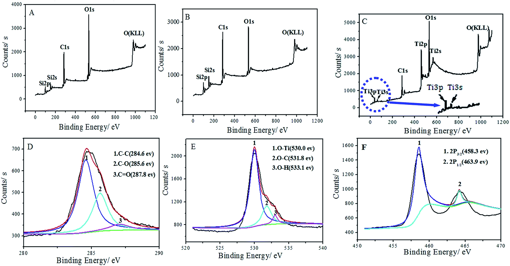 | ||
| Fig. 3 The survey XPS data for GO (A), Gr (B) and TiO2–Grs (C); the deconvolution of C1s (D), O1s (E) and Ti2p (F) spectra of TiO2–Gr composite grown by applying 100 TiO2 ALD cycles. | ||
3.2. Electrochemical characterization of the TiO2–Gr composite
Electrochemical experiments were used to characterize the TiO2–Gr composite. Different cyclic voltammograms (CVs) at bare, Nafion–Gr, and Nafion–TiO2–Gr modified GCE in a freshly prepared solution containing 2 mM K3Fe(CN)6 in the presence of 0.1 M KCl are shown in Fig. 4A. A well-shaped CV with a peak-to-peak separation of 66 mV is observed at the bare GCE (line 1). After being modified with Nafion–Gr (line 2) and Nafion–TiO2–Gr (line 3), the intensity of all anodic and cathodic peaks decrease. The phenomena are different with our previous result16,43 which should be ascribed only to Nafion, demonstrating that the negative charged skeleton of Nafion acted as the blocking layer for the diffusion of Fe(CN)63− into the film and hindered the electron and mass transfer.44 However, at the Nafion–TiO2–Gr modified GCE, the peak current increases obviously unlike that observed at Nafion–Gr modified GCE, indicating that the introduction of the TiO2–Gr provides better conducting bridges for the electron transfer of Fe(CN)63−. | ||
| Fig. 4 (A) CVs for bare (line 1), Nafion–Gr modified (line 2) and Nafion–TiO2–Gr modified (line 3) GCE in 2 mM K3Fe(CN)6 containing 0.1 M KCl, at a scanning rate of 50 mV s−1. (B) DPASV's for 1.0 × 10⁻⁵ M each of Cd2+ and Pb2+ on Nafion–TiO2–Gr modified GCE (line a) and Nafion–Gr modified GCE (line b), respectively. The inset shows the EIS characterization of the sensing interfaces: (1) Nafion–Grs modified GCE, (2) Nafion–TiO2–Gr modified GCE. | ||
Fig. 4B shows the DPASV analytical characteristics of GCEs coated with different films, e.g., Nafion–TiO2–Grs (line a) and Nafion–Grs (line b) for Pb2+ and Cd2+ determination. The stripping voltammograms were obtained in a solution containing 1.0 × 10⁻⁵ M each of Pb2+, Cd2+ in 0.1 M acetate buffer (pH 4.5) without deaeration. The sharper and higher peak current for the target metal ions were obtained at the Nafion–TiO2–Gr modified electrode. Compared with the Nafion–Gr-coated electrode, the analytical signals are improved about 1.2-fold and 12.5-fold, respectively. This can be attributed to the following factors: (i) the change of the morphologies and the structure of interface, and (ii) modification of the interfacial electron-transfer (iii) the enhanced adsorption capacity of TiO2 coatings for heavy metal ions.45 In order to verify these possibilities, ESI, a powerful technique, was used to obtain the information on the impedance changes of the electrode surface. Compared with that of the Nafion–Grs modified electrode, the electron-transfer resistances of the Nafion–TiO2–Gr sensing platform reduce greatly (Fig. 4B insets). This is resulted from the high conductivity due to the extensive conjugated sp2 carbon network46 and TiO2 assisted ion transport.4,12
3.3. The effect of the experimental variables
The effect of the deposition potential on the peak current of Cd2+ and Pb2+ after 120 s accumulation was studied in the potential range from −1.3 V to −0.9 V. The obtained results are shown in Fig. 5A. When the accumulation potential shifts from −0.9 V to −1.2 V, the stripping peak currents increase. As the accumulation potential becomes more negative than −1.2 V, the peak current reduces obviously. To obtain a good sensitivity for both Cd2+ and Pb2+ detection, −1.2 V was used as the optimal accumulation potential for the subsequent experiment. | ||
| Fig. 5 Effect of the accumulation potential (A) and deposition time (B) on the stripping peak current of 5.0 × 10⁻⁶ M each of Cd2+ and Pb2+ on a Nafion–TiO2–Gr modified electrode. | ||
The accumulation time is another important factor that influences the sensitivity of the proposed method. As depicted in Fig. 5B, with the increase of the deposition time, the response of the stripping peak currents of 5.0 × 10⁻⁶ M Cd2+ and Pb2+ increases with the preconcentration time due to the increased amount of analytes on the Nafion–TiO2–Gr modified electrode. However, the peak current decreases after 120 s because of the rapid surface saturation, which lowers the upper detection limit. Therefore, 120 s was chosen as the optimal accumulation time.
3.4. Sensing of Pb2+ and Cd2+ at Nafion–TiO2–Gr/GCE
Calibration plots for the simultaneous determination of Cd2+ and Pb2+ on the Nafion–TiO2–Gr/GCE were achieved in 0.1 M acetate buffer by increasing Cd2+ and Pb2+ concentrations from 1.0 × 10⁻¹⁰ M to 3.2 × 10⁻⁵ M. The DPASV responses for different concentrations of Cd2+ and Pb2+ are illustrated in Fig. 6. The resulting calibration plots are linear over the range from 6.0 × 10⁻⁷ M to 3.2 × 10⁻⁵ M and 1.0 × 10⁻⁸ M to 3.2 × 10⁻⁵ M for Cd2+ and Pb2+ under the optimum conditions, respectively. The calibration curves and correlation coefficients are y = 0.3933x − 1.147, R2 = 0.9904 for Pb2+, y = 1.9375x − 2.184, R2 = 0.9878 for Cd2+, respectively (x: concentration/mol L−1, y: current/μA). Based on three times the background noise, the limits of detection were 2.0 × 10⁻⁹ M for Cd2+ and 1.0 × 10⁻¹⁰ M for Pb2+, respectively, revealing a wider or comparable linear response to Pb2+ and Cd2+. Compared with most of the previous electrochemical methods for Pb2+ and Cd2+ detection,47–50 the present method shows a comparable sensitivity. The specific features of this method are shown in Table 1. | ||
| Fig. 6 (A) the DPASV signals of Cd2+ and Pb2+ with different concentrations. (B) The linear relationship between the concentration of metals and peak current. | ||
| Metal ions | Linear range (M) | Detection limit (M) | Reference |
|---|---|---|---|
| Pb2+\ | 2.4 × 10⁻⁹ to 4.3 × 10⁻⁷ | 7.2 × 10⁻¹⁰ | 47 |
| Cd2+ | 4.4 × 10⁻⁹ to 8.1 × 10⁻⁷ | 8.9 × 10⁻⁹ | |
| Pb2+\ | 1.0 × 10⁻⁵ to 1.0 × 10⁻⁴ | 2.7 × 10⁻⁸ | 48 |
| Cd2+ | 1.0 × 10⁻⁵ to 1.0 × 10⁻⁴ | 5.2 × 10⁻⁸ | |
| Pb2+\ | 1.0 × 10⁻⁷ to 1.5 × 10⁻⁵ | 1.0 × 10⁻⁸ | 49 |
| Cd2+ | 2.5 × 10⁻⁷ to 2.5 × 10⁻⁵ | 4.0 × 10⁻⁸ | |
| Pb2+\ | 4.8 × 10⁻¹⁰ to 1.4 × 10⁻⁷ | 2.4 × 10⁻¹⁰ | 50 |
| Cd2+ | 8.9 × 10⁻¹⁰ to 1.8 × 10⁻⁷ | 8.9 × 10⁻⁹ | |
| Pb2+\ | 1.0 × 10⁻⁸ to 3.1 × 10⁻⁵ | 1.0 × 10⁻¹⁰ | Present work |
| Cd2+ | 6.0 × 10⁻⁷ to 3.2 × 10⁻⁵ | 2.0 × 10⁻⁹ |
3.5. Tolerance of composites for foreign substances
Under the optimum conditions, the effect of several possible interfering substances, such as Ag+, Hg2+, Cr3+, Co2+, Zn2+, Ca2+ and Fe3+ on the Pb2+ and Cd2+ sensor based on the Nafion–TiO2–Gr/GCE was investigated when the concentration of Pb2+ and Cd2+ were 1.0 × 10⁻⁵ M. Table 2 shows the results by adding 2.0 × 10⁻⁴ M of the above metals. It can be found that Ag+, Cr3+, Zn2+, Ca2+, Fe3+, Hg2+ and Co2+ have no effect on the assay.| Substances (%) | Determination ions | Change of ΔIp |
|---|---|---|
| Ag+ | Pb2+\ | +4.75 |
| Cd2+ | −5.52 | |
| Cr3+ | Pb2+\ | −3.58 |
| Cd2+ | +5.29 | |
| Ca2+ | Pb2+\ | −6.78 |
| Cd2+ | −4.89 | |
| Zn2+ | Pb2+\ | −5.89 |
| Cd2+ | +5.44 | |
| Fe3+ | Pb2+\ | −7.98 |
| Cd2 | −5.42 | |
| Co2+ | Pb2+\ | −9.68 |
| Cd2 | +6.64 | |
| Hg2+ | Pb2+\ | +0.89 |
| Cd2 | +8.99 |
4. Conclusions
In summary, a facile and fast method was successfully developed to fabricate TiO2–Gr hybrid nanostructures by ALD method with conveniently and highly controlled thickness for TiO2. Ultrasensitive electrochemical detection of Pb(II) and Cd(II) based on the composite was established. Nafion–TiO2–Grs exhibited good electrocatalytic activity towards the oxidation of Pb and Cd. The peak currents possess a linear relationship with the concentration of Pb2+ in the range of 1.0 × 10⁻⁸ to 3.2 × 10⁻⁵ M with a detection limit of 1.0 × 10⁻¹⁰ M, and of Cd2+ in the range of 6.0 × 10⁻⁷ to 3.2 × 10⁻⁵ M with a detection limit of 2.0 × 10⁻⁹ M, respectively. To the best of our knowledge, this is the first report that electrode materials prepared by graphene with TiO2 by ALD was applied for electroanalytical determination of heavy metals. ALD can open up new avenues to synthesize other multifunctional graphene materials with excellent photochemical or electrochemical properties.Acknowledgements
This research work was supported by the National Natural Science Foundation of China (no. 21175086, 81241137 and 21275093) by the Science and Technology Innovation Fund of Shanxi Medical University (no. 01201305), Research Project Supported by Shanxi Scholarship Council of China (2013-152), the Hundred Talent Program of the Chinese Academy of Sciences, and the Hundred Talent Program of Shanxi Province.Notes and references
- S. G. Penn, L. He and M. J. Natan, Curr. Opin. Chem. Biol., 2003, 7, 609 CrossRef CAS PubMed.
- S. J. Guo and S. J. Dong, Chem. Soc. Rev., 2011, 40, 2644 RSC.
- A. Z. Shabi and H. S. Jae, Int. J. Electrochem. Sci., 2014, 9, 4598 Search PubMed.
- G. Armstrong, A. R. Armstrong, P. G. Bruce, P. Reale and B. Scrosati, Adv. Mater., 2006, 18, 2597 CrossRef CAS.
- A. R. Armstrong, G. Armstrong, J. Canales and P. G. Bruce, Angew. Chem., Int. Ed., 2004, 43, 2286 CrossRef CAS PubMed.
- M. Zukalova, M. Kalbac, L. Kavan, I. Exnar and M. Gratzel, Chem. Mater., 2005, 17, 1248 CrossRef CAS.
- Y. K. Zhou, L. Cao, F. B. Zhang, B. L. He and H. L. Li, J. Electrochem. Soc., 2003, 150, A1246 CrossRef CAS PubMed.
- Y. S. Hu, L. Kienle, Y. G. Guo and J. Maier, Adv. Mater., 2006, 18, 1421 CrossRef CAS.
- E. Baudrin, S. Cassaignon, M. Koesch, J. P. Jolivet, L. Dupont and J. M. Tarascon, Electrochem. Commun., 2007, 9, 337 CrossRef CAS PubMed.
- C. H. Jiang, I. Honma, T. Kudo and H. S. Zhou, Electrochem. Solid-State Lett., 2007, 10, A127 CrossRef CAS PubMed.
- M. A. Reddy, M. S. Kishore, V. Pralong, V. Caignaert, U. V. Varadaraju and B. Raveau, Electrochem. Commun., 2006, 8, 1299 CrossRef CAS PubMed.
- J. Moskon, R. Dominko, M. Gaberscek, R. Cerc-Korosec and J. Jamnik, J. Electrochem. Soc., 2006, 153, A1805 CrossRef CAS PubMed.
- K. S. Novoselov, V. I. Fal'ko, L. Colomb, P. R. Gellert, M. G. Schwab and K. Kim, Nature, 2012, 490, 192 CrossRef CAS PubMed.
- P. Laaksonen, M. Kainlauri, T. Laaksonen, A. Shchepetov, H. Jiang, J. Ahopelto and M. B. Linder, Angew. Chem., Int. Ed., 2010, 49, 4946 CrossRef CAS PubMed.
- Y. Ohno, K. Maehashi and K. Matsumoto, J. Am. Chem. Soc., 2010, 132, 18012 CrossRef CAS PubMed.
- H. F. Zhang, Y. J. Han, Y. J. Guo and C. Dong, J. Mater. Chem., 2012, 22, 23900 RSC.
- J. Q. Liu, J. G. Tang and J. J. Gooding, J. Mater. Chem., 2012, 22, 12435 RSC.
- S. Alwarappan, S. Boyapalle, A. Kumar, C. Z. Li and S. Mohapatra, J. Phys. Chem. C, 2012, 116, 6556 CAS.
- E. Färm, S. Lindroos, M. Ritala and M. Leskelä, Chem. Mater., 2012, 24, 275 CrossRef.
- X. Meng, Y. Zhong, Y. Sun, M. N. Banis, R. Li and X. Sun, Carbon, 2011, 49, 1133 CrossRef CAS PubMed.
- J. A. Lewis and S. M. Cohen, Inorg. Chem., 2004, 43, 6534 CrossRef CAS PubMed.
- B. M. Bridgewater and G. Parkin, J. Am. Chem. Soc., 2000, 122, 7140 CrossRef CAS.
- M. A. El Mhammedi and M. Achak, J. Hazard. Mater., 2009, 161, 55 CrossRef CAS PubMed.
- C. Gao, X. Y. Yu, R. X. Xu, J. H. Liu and X. J. Huang, ACS Appl. Mater. Interfaces, 2012, 4, 4672 CAS.
- J. A. Rodrigues, C. M. Rodrigues, P. J. Almeida, I. M. Valente, L. M. Goncalves, R. G. Compton and A. A. Barros, Anal. Chim. Acta, 2011, 701, 152 CrossRef CAS PubMed.
- M. S. A. Shah, A. R. Park, K. Zhang, J. H. Park and P. J. Yoo, ACS Appl. Mater. Interfaces, 2012, 4, 3893 Search PubMed.
- X. Sun, M. Xie, G. K. Wang, H. T. Sun, A. S. Cavanagh, J. J. Travis, S. M. George and J. Lian, J. Electrochem. Soc., 2012, 159, A364 CrossRef CAS PubMed.
- P. Y. Dong, Y. H. Wang, L. N. Guo, B. Liu, S. Y. Xin, J. Zhang, Y. R. Shi, W. Zeng and S. Yin, Nanoscale, 2012, 4, 4641 RSC.
- T. W. Lu, R. B. Zhang, C. Y. Hu, F. Chen, S. W. Duo and Q. H. Hu, Phys. Chem. Chem. Phys., 2013, 15, 12963 RSC.
- W. Hummers and R. J. Offeman, J. Am. Chem. Soc., 1958, 80, 1339 CrossRef CAS.
- X. B. Meng, D. S. Geng, J. Liu, R. Y. Li and X. L. Sun, Nanotechnology, 2011, 22, 165602 CrossRef PubMed.
- X. Sun, M. Xie, J. J. Travis, G. K. Wang, H. T. Sun, J. Lian and S. M. George, J. Phys. Chem. C, 2013, 117, 22497 CAS.
- C. M. Ban, M. Xie, X. Sun, J. J. Travis, G. K. Wang, H. T. Sun, A. C. Dillon, J. Lian and S. M. George, Nanotechnology, 2013, 24, 424002 CrossRef PubMed.
- A. V. Murugan, T. Muraliganth and A. Manthiram, Chem. Mater., 2009, 21, 5004 CrossRef CAS.
- S. Sakthive and H. Kisch, Angew. Chem., Int. Ed., 2003, 42, 4908 CrossRef PubMed.
- H. Zhang, X. J. Lv, Y. M. Li, Y. Wang and J. H. Li, ACS Nano, 2010, 4, 380 CrossRef CAS PubMed.
- S. Park, J. H. An, R. D. Piner, I. Jung, D. X. Yang, A. Velamakanni, S. T. Nguyen and R. S. Ruoff, Chem. Mater., 2008, 20, 6592 CrossRef CAS.
- Y. Wen, H. Ding and Y. Shan, Nanoscale, 2011, 3, 4411 RSC.
- B. S. Huang, H. H. Tseng and M. Y. Wey, J. Ceram. Soc. Jpn., 2009, 117, 753 CrossRef CAS.
- X. B. Yan, B. K. Tay and Y. Yang, J. Phys. Chem. B, 2006, 110, 25844 CrossRef CAS PubMed.
- G. M. An, W. H. Ma, Z. Y. Sun, Z. M. Liu, B. X. Han, S. D. Miao, Z. J. Miao and K. L. Ding, Carbon, 2007, 45, 1795 CrossRef CAS PubMed.
- Q. Wang, D. Yang, D. M. Chen, Y. B. Wang and Z. Y. Jiang, J. Nanopart. Res., 2007, 9, 1087 CrossRef CAS.
- H. F. Zhang, S. M. Shuang, L. L. Sun, A. J. Chen, Y. Qin and C. Dong, Microchim. Acta, 2014, 181, 189 CrossRef CAS.
- H. J. Chen, Y. L. Wang, Y. Liu, Y. Z. Wang, L. Qi and S. J. Dong, Electrochem. Commun., 2007, 9, 469 CrossRef CAS PubMed.
- X. Y. Yu, Q. Q. Meng, T. Luo, Y. Jia, B. Sun, Q. X. Li, J. H. Liu and X. J. Huang, Sci. Rep., 2013, 3, 2886 Search PubMed.
- Y. C. Si and E. T. Samulski, Nano Lett., 2008, 8, 1679 CrossRef CAS PubMed.
- S. Prakash and V. K. Shahi, Anal. Methods, 2011, 3, 2134 RSC.
- M. Mališić, A. Janošević, B. Š. Paunković, I. Stojković and G. Ćirić-Marjanović, Electrochim. Acta, 2012, 74, 158 CrossRef PubMed.
- C. G. Hu, K. B. Wu, X. Dai and S. S. Hu, Talanta, 2003, 60, 17 CrossRef CAS.
- L. Chen, Z. H. Su, X. H. He, Y. Liu, C. Qin, Y. P. Zhou, Z. Li, L. H. Wang, Q. J. Xie and S. Z. Yao, Electrochem. Commun., 2012, 15, 34 CrossRef CAS PubMed.
| This journal is © The Royal Society of Chemistry 2015 |