
 Open Access Article
 This Open Access Article is licensed under a
 Creative Commons Attribution 3.0 Unported Licence
Through-holes, cavities and perforations in polydimethylsiloxane (PDMS) chips
Tomas
Silva Santisteban
ab,
Roland
Zengerle
bc and
Matthias
Meier
*ab
aMicrofluidic and Biological Engineering, IMTEK – Department of Microsystems Engineering, University of Freiburg, Georges-Koehler-Allee 103, 79110 Freiburg, Germany. E-mail: matthias.meier@imtek.de
bBIOSS – Centre for Biological Signalling Studies, University of Freiburg, Germany
cLaboratory for MEMS Applications, IMTEK – Department of Microsystems Engineering, University of Freiburg, Germany
First published on 22nd September 2014
Abstract
We present a method to fabricate through-holes between 10 to 180 μm between polydimethylsiloxane (PDMS) layers of microfluidic large-scale integration platforms. Therefore we employed standard PDMS spin-coating processes onto silicon molds with microstructures formed from SU-8 and AZ photoresists. Our approach is based on the modification of the surface polarity of the PDMS prototyping molds by a 250 nm thick layer of octafluorocyclobutane (C4F8), which resulted in a contact angle of 125 ± 3° for water. This super hydrophobic surface repelled PDMS from microstructures protruding out of the spin coated PDMS layer. Subsequently, we applied and characterized the C4F8 coating for the robust fabrication of interlayer connectors between PDMS membranes of 40 μm thickness. To enable embedding of through-holes, perforations and/or cavities in very thin layers of PDMS (<20 μm) we mixed PDMS with a PDMS based silicone oil to reduce its viscosity. In contrast to previous attempts to lower the viscosity of PDMS using organic solvents, the silicone oil cross-linked to PDMS and was thus, unable to freely diffuse into the polymerized PDMS. This reduces the risk for bleeding of hazardous components in biological applications. Finally, we manufactured a three layer mLSI chip with integrated cavities for catching fluorescently labeled beads and cells. The presented process parameters can easily be adapted to specific needs in the fabrication of multi-layer PDMS arrangements by following the systematic parameter screening.
Introduction
Microfluidic large-scale integration (mLSI) is regarded as an enabling technology for systems biology research. Since the invention of the pneumatic membrane valves on polydimethylsiloxane (PDMS) chip platforms, many different design elements including pumps, oscillators, or shift registers have been developed.1–3 The mLSI design elements were generated with standard photolithography and rapid prototyping workflows, with minimal instrumentation requirements.4 An early research goal for mLSI technologies was to maximize the integration density of design elements. Although this density continuously increased, a natural limit is set by the dimensions of the object of study, e.g. the size of a biological cell.5 Therefore, current research is focused on the development of multilayer arrangements, which enable us to implement more functions within the same footprint, while still retaining the existing size of the design elements. However, the latter requirement is not specified anymore.6A central element to increase the density of fluid operations on PDMS chips is the interlayer connector named ‘via’.7 This through-hole enables the bridging of two flow streams at fluid cross-junctions with a minimal increase in the overall chip area. Initial manufacturing procedures of vias were based on a simple photolithography process, in which pillars on rapid prototyping molds with heights ranging from 20 to 50 μm were used. Upon spinning a PDMS membrane with a thickness lower than that of the pillar structures onto the mold, the pillars protrude out of the PDMS and leave a through-hole after layer bonding and demolding. Despite the simplicity of the process, the vias did not find entry on mLSI chip platforms as the manufacturing process is unstable. Often vias remained closed owing to the residual PDMS membranes present on top of the pillars after spin coating. Alternative manufacturing processes for vias e.g. laser drilling,8 electrochemical micromachining,9 clamping gaskets,10 dry etching,11 photolithographic surface micromachining,12 or the spatial inhibition of the PDMS curing over the via areas13 added a lot of complexity to the manufacturing process.
The production of perforated PDMS membranes (PMs) also presents us with similar problems. In fact, PMs can be regarded as arrays of via elements at short pitch distances. PMs are attractive design elements to separate and trap particles or biological cells in small cavities on mLSI chips.14–16 The manufacturing protocols for PMs are similar to those for via elements, with the exception that most applications demand PDMS membranes that are <20 μm thick. Thinner PDMS membranes are obtained by mixing PDMS with organic solvents to decrease its viscosity during the spin coating process.17,18 However, after the curing process, the residual organic solvents in the PDMS make the prototyping method incompatible for biological cell culture devices. Therefore, a simple manufacturing process for generating through-holes within the PDMS layers could leverage the application of vias and perforated membranes.
Here, we present a two-step manufacturing procedure for the production of reliable vias and perforated PDMS membranes with thicknesses ranging from 10 to 40 μm for microfluidic large-scale integration technologies. In the first step, we altered the surface properties of standard silicon molds with octafluorocyclobutane (C4F8) for rapid PDMS prototyping and systematically determined the range of process parameters enabling reliable implementation of via elements. In the second step, we reduced the PDMS viscosity with biologically compatible silicone oil to obtain thin perforated membranes. These simplified protocols can be combined to build robustly complex fluid routing operations or biological cell sorting systems, and trapping elements in multi-layered PDMS chips.
Experimental design
Within this work we designed and fabricated two PDMS chips, i.e. one with via elements and another with a perforated membrane, which required two or three PDMS layers, respectively. The cross sections and PDMS layer arrangement of both chips are depicted in Fig. 1.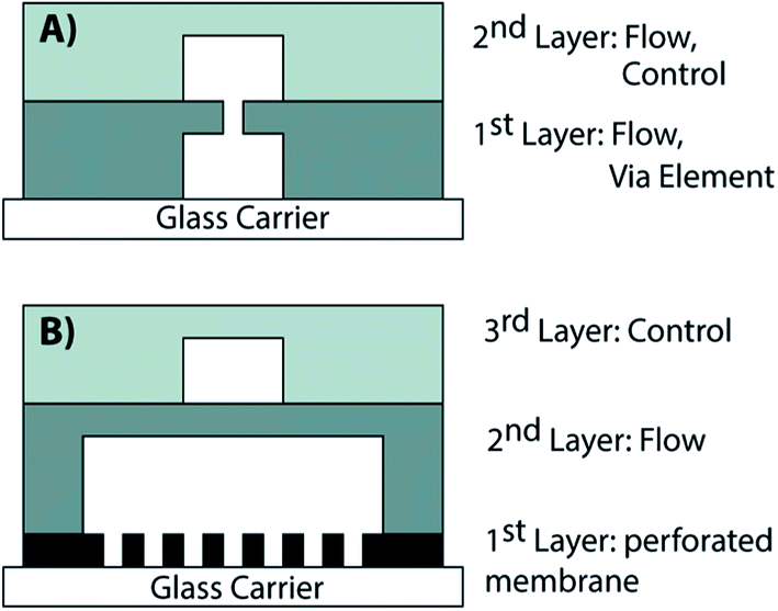 | ||
| Fig. 1 PDMS layer arrangement for via and perforated membrane fabrication. (A) The via element is included as through-hole within the lower PDMS layer. (B) The perforated membrane is included within the mLSI chip as bottom layer and acts as an array of microcavities. The here presented production process can alternatively be applied for including the perforated membrane between the fluid flow and pneumatic control layer. | ||
Design and fabrication of the PDMS molds
Chip layouts were drawn in AutoCAD and ordered as emulsion masks (bvm.maskshop, Obertshausen, Germany) with a resolution of 50.000 dpi. For each PDMS layer a silicon mold was fabricated. Chip with vias: microstructures on the mold for the 1st PDMS layer were 120 × 20 μm (width × height) and fabricated with the photoresist AZ-40XT (MicroChemicals, Germany). To obtain a semi-round channel profile, the AZ photoresist were refloated for 4 h at 200 °C on a hot plate. On top of the AZ layer, SU-8 (microchem, MI, USA) microstructures with the shapes of round pillars were deposited in order to implement via elements. The pillar sizes changed between chips (see below). Microstructures on the silicon mold for the 2nd PDMS layer were fabricated with SU-8 and had a width and height of 120 and 40 μm, respectively. Chip with perforated membrane: microstructures on the mold for 1st PDMS layer forming the perforated membrane were fabricated by SU-8, and had a width and height of 180 μm and 40 μm, respectively. Microstructures on mold for the 2nd and 3rd PDMS, resembled the manufacturing processes for production of the molds for the 1st and 2nd PDMS layer of the chip with via elements expect that the SU-8 layer for the vias elements were omitted.Coating of the PDMS molds
All molds were coated with a 250 nm octafluorocyclobutane (C4F8) layer that was deposited by an ion induced plasma (ICP) process. The parameters for the deposition process within the ICP machine (Surface Technology Systems, Newport, UK) were 600 W for the RF coil, a manual pressure of 65% in the deposition chamber, and a deposition rate of 85 standard cubic centimeter per minute (sccm) for the C4F8. Alternatively, it is possible to deposit C4F8 within a regular plasma oxidation chamber.Prototyping of the PMDS chip with via elements
Via elements were included within a chip with two PDMS layers, where layers were bonded together with the off-ratio method.19 Briefly, the upper and lower PDMS layer had a 5![[thin space (1/6-em)]](https://www.rsc.org/images/entities/char_2009.gif) :1 and 20:1 ratio of the Sylgard 184 (Dow Corning, Midland, MI) base material to the cross-linker, respectively. The optimal spin parameters for the lower via layer were determined as given below. Both the layers were half-cured for 15–18 minutes at 80 °C. After the alignment of the layers, the chip was heated for another 60 minutes at 80 °C before it was plasma bonded to the glass carrier.
:1 and 20:1 ratio of the Sylgard 184 (Dow Corning, Midland, MI) base material to the cross-linker, respectively. The optimal spin parameters for the lower via layer were determined as given below. Both the layers were half-cured for 15–18 minutes at 80 °C. After the alignment of the layers, the chip was heated for another 60 minutes at 80 °C before it was plasma bonded to the glass carrier.
Prototyping of PDMS chips with perforated membranes
The PDMS chips with PMs comprised three layers. The PM was incorporated as the bottom layer. The PMs were fabricated with Sylgard 184 (10:1) mixed with different ratios of the silicone oil Element 14 PDMS 50-E (Momentive, USA), a low viscosity PDMS-based oil. The top two PDMS layers were fabricated and bonded to each other using a procedure similar to that for the via chips. The PM was bonded to the upper two layers by plasma activation.
Results and discussion
Via structure elements
Standard mold fabrication protocols for PDMS end with a silanization step.20 Silane acts as a lubricant layer and improves the release of PDMS by reducing the surface energy of the silicon wafer and the patterned photoresist features on it. While this method is sufficient for robustly demolding the PDMS, it is not sufficient for avoiding the residual PDMS on top of SU-8 via elements during a spin coating process, especially at small margins. Therefore, we replaced the silane coating with a C4F8 coating. It has been reported that the SU-8 surfaces and the silane coated SU-8 have water contact angles between 75 and 100°. For a silicon mold coated with 250 nm C4F8 layer, we determined the water surface contact angle to be 125 ± 3°. In order to investigate if this change in the surface energy changed the wettability of the PDMS on the SU-8 poles for via construction, we fabricated two-layered microfluidic chips with a simple 2-dimensional crossing channel network (see Fig. 2B). During the fabrication process, we systematically determined the mutual dependence between the spin rates for the coating molds with uncured PDMS and the protrusion height of the poles on the mold for the production of functional via elements. In particular, three molds for the lower PDMS layer were manufactured with pole heights of 55, 77, and 100 μm, respectively.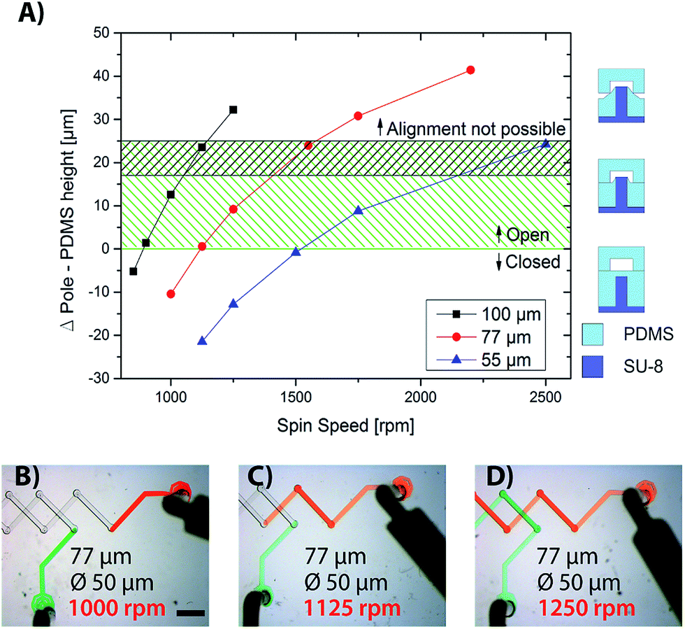 | ||
| Fig. 2 Mutual dependence of the PDMS layer thickness and the protrusion pole height for the fabrication of vias within the two-layered PDMS chips. (A) The plot shows the protrusion heights of the poles (55, 77, and 100 μm) from the PDMS layers spin coated for 30 seconds at various spin speeds. The resulting height of the PDMS layer formed by the 20:1 ratios was calculated from the reference values, whereas the pole heights were experimentally measured. The green and green/black dashed areas denote the parameter space for the open via elements on the C4F8 and silane coated molds. The pictograms on the right site of the figure illustrate the different layer alignment regimes. (B–D) Images of the two-layered PDMS chips with 2D crossing flow channels enabled by via elements. The via elements are closed, not robustly open, and open within the figures B, C, and D, respectively. The flow channels are filled with green and red colored aqueous solutions. The scale bar in figure B corresponds to 1 mm. | ||
The result is shown in Fig. 2A, where we have plotted the length of the SU-8 pole that protrudes from the PDMS layer, i.e., the difference between the height of the SU-8 pole and the thickness of the PDMS layer, versus the spin speed used to coat molds with uncured PDMS. The absolute height of the PDMS layer was between 25 and 125 μm at 750 and 2500 rpm, respectively, and was calculated from the spin-coating speed, by considering reference values.21 Clearly, when the height difference between the poles and the PDMS is <0 μm, the SU-8 poles are completely covered by the PDMS, and the vias remain closed. Upon slightly decreasing the height of the PDMS layer relative to the pole height, the vias remained open. When the height difference between the poles and PDMS layer is more than 25 μm, the top and lower PDMS layers get misaligned owing to the steric hindrance of the poles as illustrated in the pictograms of Fig. 2A. Although we countered the poles on the flow layer with complementary holes (diameter: 250 μm; depth: 40 μm) in the upper PDMS layer, the bonding of the two PDMS layers was hindered. The green dashed area shows the parameter region for the functional robust fabrication of vias onto the C4F8 coated molds.
For comparison, we screened the same parameter space for the production of vias on the silanated PDMS molds. The green/black shaped area in Fig. 2A indicates the region from where the functional vias were obtained. This result makes an argument that a change in the surface property causes the repulsion of the PDMS from the pole tops. A change of the C4F8 layer thickness from 100 to 500 nm was neither changing the water contact angle on the surface nor did affect the PDMS de-molding process. In conclusion, the C4F8 coating on the PDMS prototyping molds increases the parameter region for the production of vias. This study offers a method for the fabrication of through-holes in the thinner PDMS layers.
Perforated PDMS membranes
PDMS membranes with film thicknesses ≤20 μm have been fabricated by lowering the viscosity of the PDMS base material with organic solvents during the spin-coating process. The prototyping of thin perforated membranes failed either owing to the rupture of the membrane during demolding or because of the incomplete removal of PDMS from the pole structures. It has been previously shown22 that the wettability of the molds with dense feature structures (unlike the wettability of the via elements) changes with respect to the aspect ratio, area, and pitch distance of the features. Therefore, we tested if the C4F8 coating of molds with an array of SU-8 poles can be used for the fabrication of perforated PDMS membranes.To achieve this, we designed an mLSI chip with a PM on a glass substrate forming cavities as the retaining structure for the beads or cells. The chip layout is shown in Fig. 3D where the bottom, middle, and top layer are the PM, flow and control layer, respectively. The PM was prototyped from an array of SU-8 poles with a diameter, height, and pitch distance of 20, 20, and 40 μm respectively; the total array size was 4 mm × 4 mm. To achieve a PM thickness of <20 μm, we lowered the viscosity of the PDMS with the silicone oil Element 14 PDMS 50-E. Due to its PDMS basis we assumed that the components of the silicon oil are permanently cross-links within the Pt catalyzed curing process to the base material of the PDMS. To test this we performed a swelling experiment. For this PDMS blocks with a weight ratio of 6.5; 1; 2.5 of PDMS base material, curing agent, silicon oil respectively were swelled in chloroform for 24 hours at RT. The samples were thereafter dried for 24 hours at 80 °C. The gel fraction, which is the weight after extraction and drying to the initial weight of the DPMS blocks with the silicon oil was 85.1 ± 1.9. Reference PDMS blocks without the silicon oil had a gel fraction of 91 ± 1.9%, which is in agreement with previous reported gel fraction for off-ratio cured PDMS.23 Thus we inferred that the silicon oil indeed is cross-liked to the PDMS base unlike organic solvents.
 | ||
| Fig. 3 Fabrication of the perforated PDMS membranes with different mass ratios of silicone oil from the C4F8 coated molds. (A) The plot shows the spin speeds required to obtain open through-holes within the PDMS layers, with different mass ratios of the silicone oil. The wafer with the array of 20 μm high SU-8 pillars was coated with C4F8 before usage. Black, red, and blue dots denote the parameters at which the through-holes in the cured PMDS were closed and opened, or when the chip could not be assembled due to the steric hindrance of the protruding pillars. (B) and (C) Images of the PDMS layer (16 and 12 μm in height) with closed and open through-holes. (D) Image of a three-layered PDMS chip with a perforated PDMS membrane on top of a glass chip at the bottom forming cavities for retaining beads. The inset shows a zoomed-in view of the perforated membrane at the bottom of a microchamber. The holes/pores were filled with fluorescently labeled beads. The scale bars in figure B, C, and D denote for 5, 5, and 750 μm, respectively. | ||
The addition of Element 14 PDMS 50-E did not change the curing times of Sylgard 184. We determined the optimal mass ratio between the silicone oil and PDMS, XOil, and the corresponding spin speeds of the spin coating process, in order to achieve open through-holes within the thin PDMS membranes.
For each XOil, a chip was fabricated, and then horizontally cut to examine the state of the through-holes and to check whether they were open or closed. The result is shown in Fig. 3A. In the case of XOil, the ratios were between 0.25 and 0.35, and it was possible to obtain fully functional open through-holes demolded from a pole array. Below an XOil value of 0.25, the through-holes remained closed, whereas above a value of 0.35, the pole protrusion started hindering the process of layer bonding. Interestingly, increasing the spin speed from 1000 to 1600 rpm did not lead to a further thinning of the membrane, which indicates that the height of the PDMS membrane within this regime is predominantly set by the XOil ratio. For example we found that for a XOil ratio of 0.3 the PDMS membrane thickness was 12 ± 3 μm.
To demonstrate the function of PMs within the fully assembled mLSI chip, we captured fluorescently labeled beads with a diameter of 10 μm. Beads with a concentration of 106 mL−1 were flushed through the four microchambers of the mLSI platform with a flow rate of 1 μL min−1. Interrupting the flow allowed the beads to settle within the holes of the PM at the bottom of the chip. 82% of the holes were occupied with a bead after restarting and stopping the flow of the bead solution thrice for a period of 1 minute. The geometry of the pore array within the mLSI chip layout was not optimized for obtaining a high degree of bead occupancy. It is expected that in conjugation with the pillars and the other flow line barriers, higher degrees of cell or bead occupancies are achievable.
In conclusion, we experimentally demonstrated the advantage of using a simple super-hydrophobic coating procedure for PDMS molds. This technique could be used to fabricate through-holes/via elements as well as perforated thin PDMS sheets at a higher density for microfluidic large-scale integrated chip platforms. The C4F8 coatings have been used previously for the production of high aspect ratio24 for the coating of PDMS, and for increasing the hydrophobicity of the material.25 We show that reducing the surface energy of the wafer and photoresist lead to robust release properties of PDMS. In a parallel experiment, we found the same robustness upon reducing the surface energy of the silicon molds, by coating the wafer with hydroxypropyl-methyl cellulose.26 The cellulose coating, however, is not stable over time and has to be applied before each prototyping process. Therefore, it was not characterized in detail. Moreover, for the pillar arrays with small pitch distances, the C4F8 coating could be used to produce perforated PDMS membranes. Together with the silicone oil Element 14 PDMS 50-E, we introduced an alternative to organic solvents for lowering the viscosity of PDMS and for fabricating thinner PDMS layers in the range of 10–40 μm. Both the fabrication procedures can leverage large-scale integration microfluidics. Future research in this area should focus on building more complex flow circuitries in three dimensions.
Acknowledgements
This study was supported by the German Excellence Initiative of the German Federal and State Governments (EXC-294 and GSC-4), and by the German Research Foundation (Emmy-Noether Grant ME3823/1-1).References
- J. Melin and S. R. Quake, Annu. Rev. Biophys. Biomol. Struct., 2007, 36, 213–231 CrossRef CAS PubMed
.
- P. N. Duncan, T. V. Nguyen and E. E. Hui, Proc. Natl. Acad. Sci. U. S. A., 2013, 110, 18104–18109 CrossRef CAS PubMed
- N. S. G. K. Devaraju and M. A. Unger, Lab Chip, 2012, 12, 4809 RSC
- J. McDonald and G. Whitesides, Acc. Chem. Res., 2002, 35, 491–499 CrossRef CAS PubMed
- M. Meier, R. Sit, W. Pan and S. R. Quake, Anal. Chem., 2012, 84, 9572–9578 CrossRef CAS PubMed
- J. A. Weaver, J. Melin, D. Stark, S. R. Quake and M. A. Horowitz, Nat. Phys., 2010, 6, 218–223 CrossRef CAS
- E. P. Kartalov, C. Walker, C. R. Taylor, W. F. Anderson and A. Scherer, Proc. Natl. Acad. Sci. U. S. A., 2006, 103, 12280–12284 CrossRef CAS PubMed
- J. Huft, D. J. Da Costa, D. Walker and C. L. Hansen, Lab Chip, 2010, 10, 2358 RSC
- N. Qu, X. Chen, H. Li and D. Zhu, Int. J. Adv. Des. Manuf. Technol., 2014, 72, 487–494 CrossRef PubMed
- J. Choi, K.-H. Lee and S. Yang, J. Micromech. Microeng., 2011, 21, 097001 CrossRef
- A. L. Thangawng, R. S. Ruoff, M. A. Swartz and M. R. Glucksberg, Biomed. Microdevices, 2007, 9, 587–595 CrossRef CAS PubMed
- W. Chen, R. H. W. Lam and J. Fu, Lab Chip, 2011, 12, 391–395 RSC
- C. F. Carlborg, T. Haraldsson, M. Cornaglia, G. Stemme and W. van der Wijngaart, J. Microelectromech. Syst., 2010, 19, 1050–1057 CrossRef CAS
- J. R. Rettig and A. Folch, Anal. Chem., 2005, 77, 5628–5634 CrossRef CAS PubMed
- H. Wei, B.-H. Chueh, H. Wu, E. W. Hall, C.-W. Li, R. Schirhagl, J.-M. Lin and R. N. Zare, Lab Chip, 2011, 11, 238 RSC
- Y. Wang, P. Shah, C. Phillips, C. E. Sims and N. L. Allbritton, Anal. Bioanal. Chem., 2011, 402, 1065–1072 CrossRef PubMed
- A. L. Thangawng, R. S. Ruoff, M. A. Swartz and M. R. Glucksberg, Biomed. Microdevices, 2007, 9, 587–595 CrossRef CAS PubMed
- J. H. Koschwanez, R. H. Carlson and D. R. Meldrum, PLoS One, 2009, 4, e4572 Search PubMed
- M. A. Unger, H. P. Chou, T. Thorsen, A. Scherer and S. R. Quake, Science, 2000, 288, 113–116 CrossRef CAS
- J. R. Anderson, D. T. Chiu, R. J. Jackman, O. Cherniavskaya, J. C. McDonald, H. Wu, S. H. Whitesides and G. M. Whitesides, Anal. Chem., 2000, 72, 3158–3164 CrossRef CAS
- W. Y. Zhang, G. S. Ferguson and S. Tatic-Lucic, IEEE, Elastomer-supported cold welding for room temperature wafer-level bonding, 2004, pp. 741–744 Search PubMed.
- C. Greiner, A. del Campo and E. Arzt, Langmuir, 2007, 23, 3495–3502 CrossRef CAS PubMed
- F. B. Madsen, I. Dimitrov, A. E. Daugaard, S. Hvilsted and A. L. Skov, Polym. Chem., 2013, 4, 1700–1707 RSC
- L.
P. Yeo, Y. H. Yan, Y. C. Lam and M. B. Chan-Park, Langmuir, 2006, 22, 10196–10203 CrossRef CAS PubMed
- A. D. Tserepi, M.-E. Vlachopoulou and E. Gogolides, Nanotechnology, 2006, 17, 3977–3983 CrossRef CAS
- L. Gitlin, P. Schulze and D. Belder, Lab Chip, 2009, 9, 3000 RSC
| This journal is © The Royal Society of Chemistry 2014 |