
Tuning nanoscale morphology using mixed solvents and solvent vapor treatment for high performance polymer solar cells†
Dun Wanga,
Fujun Zhang*a,
Lingliang Lia,
Jiangsheng Yub,
Jian Wanga,
Qiaoshi Ana and
Weihua Tang*b
aKey Laboratory of Luminescence and Optical Information, Ministry of Education, Beijing Jiaotong University, Beijing, 100044, P. R. China. E-mail: fjzhang@bjtu.edu.cn
bKey Laboratory of Soft Chemistry and Functional Materials, Ministry of Education, Nanjing University of Science and Technology, Nanjing, 210094, China
First published on 24th September 2014
Abstract
A series of high performance polymer solar cells (PSCs) were fabricated with poly[(4,8-bis-(2-ethylhexyloxy)-benzo[1,2-b:4,5-b′](dithiophene)-2,6-diyl-alt-(4-(2-ethylhexanoyl)-thieno [3,4-b]thiophene)-2,6-diyl] (PBDTTT-EFT) as the donor and with [6,6]phenyl-C71-butyric acid methyl ester (PC71BM) as the acceptor. The PSCs processed with DCB/CB mixed solvents show an open circuit voltage (Voc) of 0.79 V, a short circuit current density (Jsc) of 13.63 mA cm−2 and a fill factor (FF) of 62.9%, resulting in the highest PCE of 6.77% compared with a PCE of 5.99% for CB as a solvent and a PCE of 5.39% for DCB as a solvent. The PCE of PSCs processed with DCB/CB mixed solvents is further increased to 7.58% from 6.77% by chloroform vapor annealing treatment for 60 seconds. The PCE improvement should be attributed to the optimized bi-continuous interpenetrating networks of PBDTTT-EFT:PC71BM for better exciton dissociation and charge carrier collection.
Introduction
Polymer solar cells (PSCs) are promising candidates for future photovoltaic devices to solve the energy crisis due to their many advantages, such as flexibility, environmental friendliness, and easy large-area applications.1–4 Bulk-heterojunction PSCs, typically consisting of an active layer with a donor–acceptor (D–A) blend films, have attracted significant attention for obtaining high power conversion efficiency (PCE) up to 8–9%.5,6 The strategy for PCE improvement of bulk-heterojunction PSCs could be summarized as the following: (i) synthesis novel narrow band gap materials with broad absorption capabilities and high photon harvesting efficiency,7,8 (ii) finely tuning the nanoscale morphology of D–A to form bi continuous interpenetrating networks in the active layer,9,10 (iii) ternary materials for widen photon harvesting range11,12 and (iv) selecting interfacial layers for better charge carriers collection.13 Recently, conjugated polymers based on benzo[1,2-b:4,5-b′]dithiophene (BDT) units have attracted interest as electron donors in the PSCs due to their high yield in synthesis, suitable band gap and high charge carriers mobility.14 Among BDT-based polymers, the alternative copolymers of BDT and thieno[3,4-b]thiophene (TT), namely PBDTTTs, are an important family of photovoltaic materials. For additional improvements in the photovoltaic performance of the PBDTTTs, chemical structure modifications brought by using different substituents on BDT have been explored to further improve the efficiency. For example, several conjugated polymers like PBDTTT-C, PBDTTT-C-T, PBDTTT-E and PBDTT-E-T have been designed and applied in PSCs with high PCEs of 5–8%.15 Among them, the polymer PBDTTT-E exhibited promising photovoltaic properties due to a high short circuit current density (Jsc) of 15 mA cm−2. However, the open-circuit voltage (Voc) of PSCs based on PBDTTT-E was only 0.6 V resulting in a low PCE.16 In order to obtain a high Voc, 2-ethylhexyl-4,6-dibromo-3-fluoro-thieno[3,4-b]thiophene-2-carboxy late (EFT) was introduced to the position of the TT unit to adjust the highest occupied molecular orbital (HOMO), the novel narrow band polymer PBDTTT-EFT was synthesized.17 The functional group EFT endows the polymer with a relatively low-lying HOMO energy level, which is beneficial to obtain a relative high Voc for further performance improvement of PSCs.It is known that the performance of PSCs is strongly correlated with the morphological properties of the D–A blend films including materials miscibility, crystallinity of polymers, domain size, molecular orientation, and hierarchical structures.18–20 Therefore, the tuning morphology of the active layer should play a very important role in determining the performance of PSCs. Ideally, the bi-continuous interpenetrating networks with suitable nanodomains would determine the tradeoff between exciton dissociation and charge carriers transport to maximize charge collection. Many strategies have been carried out for improving the morphology of the blend films, such as the selection of solvent,9 solvent additive,21 using mixed solvents,22 solvent vapor and thermal annealing treatments.23–25 However, the morphology of active layer including narrow band gap polymer is hardly adjusted by thermal annealing treatment due to its poor self-packaging characteristic.26,27 Recently, Liang et al. reported an efficient method to adjust the active layer morphology by adopting mixed solvent approach.28 Dou et al. also reported that the PCE of PSCs was increased to 5.8% from 1.5% by using 1,8-diiodoctane (DIO) as solvent additive based on a blend film composed of poly{2,6′-4,8-di(5-ethylhexylthienyl)benzo[1,2-b;3,4-b]dithiophene-alt-5-dibutyloctyl-3,6-bis (5-bromothiophen-2-yl) pyrrolo[3,4-c]pyrrole-1,4-dione} (PBDTP-DPP) donor and [6,6]phenyl-C71-butyric acid methyl ester (PC71BM) acceptor.29 Gao et al. further improved the PCE up to 6.6% by utilizing chloroform/dichlorobenzene (CF/DCB) binary solvent to optimize the morphology of the PBDTP-DPP:PC71BM blend films.30 Therefore, how to screen suitable solvent system to adjust the morphology of active layer is one of the key issues in obtaining high performance PSCs.
In this paper, a series of PSCs with PBDTTT-EFT:PC71BM as the active layer were fabricated, the optimized power conversion efficiency (PCE) of 7.58% was obtained by finely adjusting morphology of PBDTTT-EFT:PC71BM blend films by different solvents and solvent vapor annealing treatment. The experimental results exhibit that the morphology of PBDTTT-EFT:PC71BM blend films plays the key role in determining the performance of PSCs. The morphological evolution of the active layer during this two-step optimization process was demonstrated by X-ray diffraction (XRD) and atomic force microscopy (AFM) measurements.
Results and discussion
The chemical structures of the PBDTTT-EFT and PC71BM are shown in Fig. 1a. The synthetic routes for the monomers and polymer were outlined in Scheme S1.† The 2-ethylhexyl-4,6-dibromo-3-fluoro-thieno[3,4-b]thiophene-2-carboxylate (EFT)31 and 2,6-bis(trimethyltin)-4,8-bis(5-(2-ethylhexyl)thiophen-2-yl)benzo[1,2-b:4,5-b′]dithiophene (BDTTT)15 were synthesized according to the similar procedure in reported literature. The alternative D–A copolymer PBDTTT-EFT was synthesized by Stille coupling reaction between BDTTT and EFT. PBDTTT-EFT exhibits excellent solubility in common organic solvents such as CF, DCB and chlorobenzene (CB) and shows a rather good thermal stability up to 343 °C under nitrogen atmosphere (ESI, Fig. S1†). The weight average molecular weight (Mw) of PBDTTT-EFT is 81.9 kDa and a polydispersity index (PDI) of 3.5, which was determined by gel permeation chromatography (GPC) analysis (ESI, Table S1†). The absorption spectra of PBDTTT-EFT and PC71BM are shown in Fig. 1c. There was no red-shifted phenomenon between the absorption of PBDTTT-EFT in DCB solution and in solid film. The maximum absorption peak of PBDTTT-EFT film locates at 707 nm, in agreement with the strong electron-deficient ability of EFT unit. The absorption edge of the polymer film is at 790 nm, corresponding to an optical bandgap (Eg) of 1.57 eV. The collected absorption data are listed in Table S2.† As shown in Fig. 1c, PBDTTT-EFT shows relative strong absorption in the range from 500 nm to 790 nm. To cover the short wavelength region, PC71BM was used as the acceptor for the PSCs. The HOMO and the lowest unoccupied molecular orbital (LUMO) energy levels of PBDTTT-EFT were determined by electrochemical cyclic voltammetry (CV) (ESI, Fig. S2†), which are −5.45 and −3.54 eV, respectively. The electrochemical bandgap of the PBDTTT-EFT is 1.91 eV, in agreement with its optical bandgap. The low lying HOMO level is favorable to generate high Voc in PSCs.32,33 The LUMO difference between PBDTTT-EFT (−3.54 eV) and PC71BM (−4.3 eV) is 0.76 eV, which can provide enough driving force for exciton dissociation.34 | ||
| Fig. 1 (a) Chemical structures of PBDTTT-EFT and PC71BM. (b) Energy level structure of PBDTTT-EFT based on PSCs. (c) Normalized absorption spectra of PBDTTT-EFT in the solid film and in DCB solution. | ||
A series of PSCs with PBDTTT-EFT:PC71BM as the active layer were designed and fabricated to investigate the effect of active layer thickness (adjusted by spin-coating speed) and mixed solvents on the photovoltaic performance of PSCs. The device structure of PSCs is shown in the Fig. 2a. More than two hundred cells were fabricated and measured to obtain the convincing data, each kind of PSCs also showed the similar performance from different batch. It is known that the balance between photon harvest and charge carrier transport strong depends on the thickness of active layer, which would determine the performance of PSCs. In order to obtain the champion performance of PSCs, 3 v% DIO was added into the blend solutions prepared by different solvents (DCB, CB or DCB/CB) prior to spin coating process. Firstly, the thickness of active layers was optimized by adjusting the spin-coating speed from 700 rpm to 900 rpm to obtain the best PCE of PSCs. The J–V characteristic curves of three kinds of PSCs processed with different solvents were measured under illumination 100 mW cm−2 AM 1.5G simulated solar light and are shown in Fig. S6.† The Voc of all PSCs was kept at 0.79 V with 0.01 V indeterminacy. As we know, the Voc of PSCs is primarily determined by two factors, (i) the energy levels difference between the HOMO of the electron donor and the LUMO of electron acceptor;35 and (ii) the work function difference between anode and cathode electrode.36,37 It can be assumed that the Voc should be kept constant because the only difference is solvent for the three kinds of PSCs. According to the Fig. S6,† each kind of PSCs with active layers processed from different solvents obtains the best performance under spin-coating speed 800 rpm conditions. The key parameters of all PSCs processed with different solvents and spin-coating speed were summarized according to their J–V characteristic curves and are listed in Table S3.† In order to more clearly exhibit the effect of solvent on the performance of PSCs, the optimized J–V characteristic curves of each kind of PSCs are shown in Fig. 2b. According to the J–V characteristic curves, the key photovoltaic parameters of the optimized PSCs are summarized in Table 1. It is apparent that the performance of PSCs were improved by using mixed solvent DCB/CB (v/v, 1![[thin space (1/6-em)]](https://www.rsc.org/images/entities/char_2009.gif) :1), compared with the PSCs processed with CB or DCB as solvent (DIO was added into solutions before the spin-coating process, v/v of solvent/DIO is 97:3), For the PSCs processed with DCB as solvent, the optimized PCE of 5.39% was obtained with the Jsc of 11.54 mA cm−2 and fill factor (FF) of 59.1%. The average PCE of PSCs processed with DCB as solvent is 5.30% evaluated from 30 cells. For the PSCs processed with CB as solvent, the optimized PCE of 5.99% was obtained with the Jsc of 13.18 mA cm−2 and FF of 58.3%. The average PCE of PSCs processed with CB as solvent is 5.86% evaluated from 30 cells, which correspond to about 10.6% PCE improvement compared with PSCs processed with DCB as solvent. According to the optimized performance of PSCs processed with CB or DCB as solvent, it is apparent that the Jsc of PSCs processed with CB as solvent is about 12.4% larger than that of PSCs processed with DCB as solvent. Meanwhile, the FF of PSCs processed with CB as solvent is slight smaller than that of PSCs processed with DCB as solvent. For the PSCs processed with mixed solvent CB/DCB, the optimized 6.77% PCE was obtained due to the more balanced improvement of Jsc of 13.63 mA cm−2 and FF of 62.9%. In order to further confirm the effect of solvent on the performance of PSCs, the EQE spectra of all PSCs were measured and are shown in Fig. 2c.
:1), compared with the PSCs processed with CB or DCB as solvent (DIO was added into solutions before the spin-coating process, v/v of solvent/DIO is 97:3), For the PSCs processed with DCB as solvent, the optimized PCE of 5.39% was obtained with the Jsc of 11.54 mA cm−2 and fill factor (FF) of 59.1%. The average PCE of PSCs processed with DCB as solvent is 5.30% evaluated from 30 cells. For the PSCs processed with CB as solvent, the optimized PCE of 5.99% was obtained with the Jsc of 13.18 mA cm−2 and FF of 58.3%. The average PCE of PSCs processed with CB as solvent is 5.86% evaluated from 30 cells, which correspond to about 10.6% PCE improvement compared with PSCs processed with DCB as solvent. According to the optimized performance of PSCs processed with CB or DCB as solvent, it is apparent that the Jsc of PSCs processed with CB as solvent is about 12.4% larger than that of PSCs processed with DCB as solvent. Meanwhile, the FF of PSCs processed with CB as solvent is slight smaller than that of PSCs processed with DCB as solvent. For the PSCs processed with mixed solvent CB/DCB, the optimized 6.77% PCE was obtained due to the more balanced improvement of Jsc of 13.63 mA cm−2 and FF of 62.9%. In order to further confirm the effect of solvent on the performance of PSCs, the EQE spectra of all PSCs were measured and are shown in Fig. 2c.
 | ||
| Fig. 2 (a) Schematic structural configuration of PSCs. (b) J–V characteristics curves of PSCs processed with different solvents under spin-coating speed 800 RPM under illumination 100 mW cm−2 AM 1.5G simulated solar light. (c) EQE spectra of PSCs processed with different solvents under spin-coating speed 800 RPM. | ||
| Solvent | Voc (V) | Jsc (mA cm−2) | FF (%) | Best PCE (%) | Ave PCE (%) | Rs (Ω cm2) | Rsh (Ω cm2) |
|---|---|---|---|---|---|---|---|
| a The average PCE values were evaluated based on 30 cells. | |||||||
| DCB | 0.79 | 11.54 | 59.1 | 5.39 | 5.30 ± 0.09 | 7.93 | 64.38 |
| CB | 0.78 | 13.18 | 58.3 | 5.99 | 5.86 ± 0.13 | 6.06 | 84.39 |
| DCB/CB | 0.79 | 13.63 | 62.9 | 6.77 | 6.70 ± 0.07 | 4.89 | 97.15 |
According to the EQE spectra of three kinds of PSCs, the PSCs processed with DCB/CB as solvent show the highest EQE values in the whole wavelength range, the maximum EQE value is about 63% at 620 nm. The calculated Jsc values by integrating the EQE data with the AM 1.5G solar spectrum were 11.21 mA cm−2, 12.9 mA cm−2 and 13.60 mA cm−2 for the PSCs processed with DCB, CB and DCB/CB solvents, respectively. This is in good agreement (within 3% error) with the experimental results obtained from J–V characteristic curves, as shown in Fig. 2b. The highest EQE of PSCs processed with mixed solvent (DCB/CB) should be attributed to forming an ideal donor and acceptor bi-continuous interpenetrating networks, resulting in the more balance of photon harvest, exciton dissociation and charge collection. This kind of balance strongly depends on the thickness of active layer and the bi-continuous interpenetrating networks in the active layer. The thicker the active layer is, the more photon could be harvested and the more charge carrier collection is limited. Therefore, the thickness of active layer plays a key role in determining the performance of PSCs. The thickness of active layer can be finely adjusted by selecting different solvent, in addition to by controlling the spin-coating speed. The absorption spectra of blend films processed with different solvents and the same spin-coating speed were measured and are shown in Fig. 3a. All blend films exhibit almost the same absorption spectral shape with three distinct absorption peaks located at 473 nm, 643 nm and 712 nm. The CB solvent is more viscous compared with DCB solvent, resulting in that the blend films processed with CB as solvent are thicker under the same spin-coating speed.26 The blend films processed with CB solvent exhibit the relative strong absorption intensity compared with that of films processed with DCB as solvent in the spectral range from 300 nm to 750 nm. The absorption intensity of the blend films can be adjusted by using mixed solvents under the same fabrication condition (800 RPM). According to the absorption spectra of blend films and EQE spectra of PSCs processed with DCB/CB as solvent, it can be demonstrated that photon-generated excitons on PBDTTT-EFT and PC71BM were demonstrated to be efficiently dissociated into free charge carriers and collected by individual electrode. The sharply decreased EQE spectra in the short wavelength range (less than 380 nm) should be attributed to the relative low transmittance of ITO substrate in this spectral range, as shown in Fig. 3a. The photoluminescence (PL) spectra of PBDTTT-EFT in different solvents are shown in Fig. 3b, the PL emission peak of PBDTTT-EFT is about 820 nm with half maximum full width 80 nm corresponding to the radiative energy about 1.51 eV. The radiative energy is very close to the optical bandgap (1.57 eV) obtained from absorption spectrum.
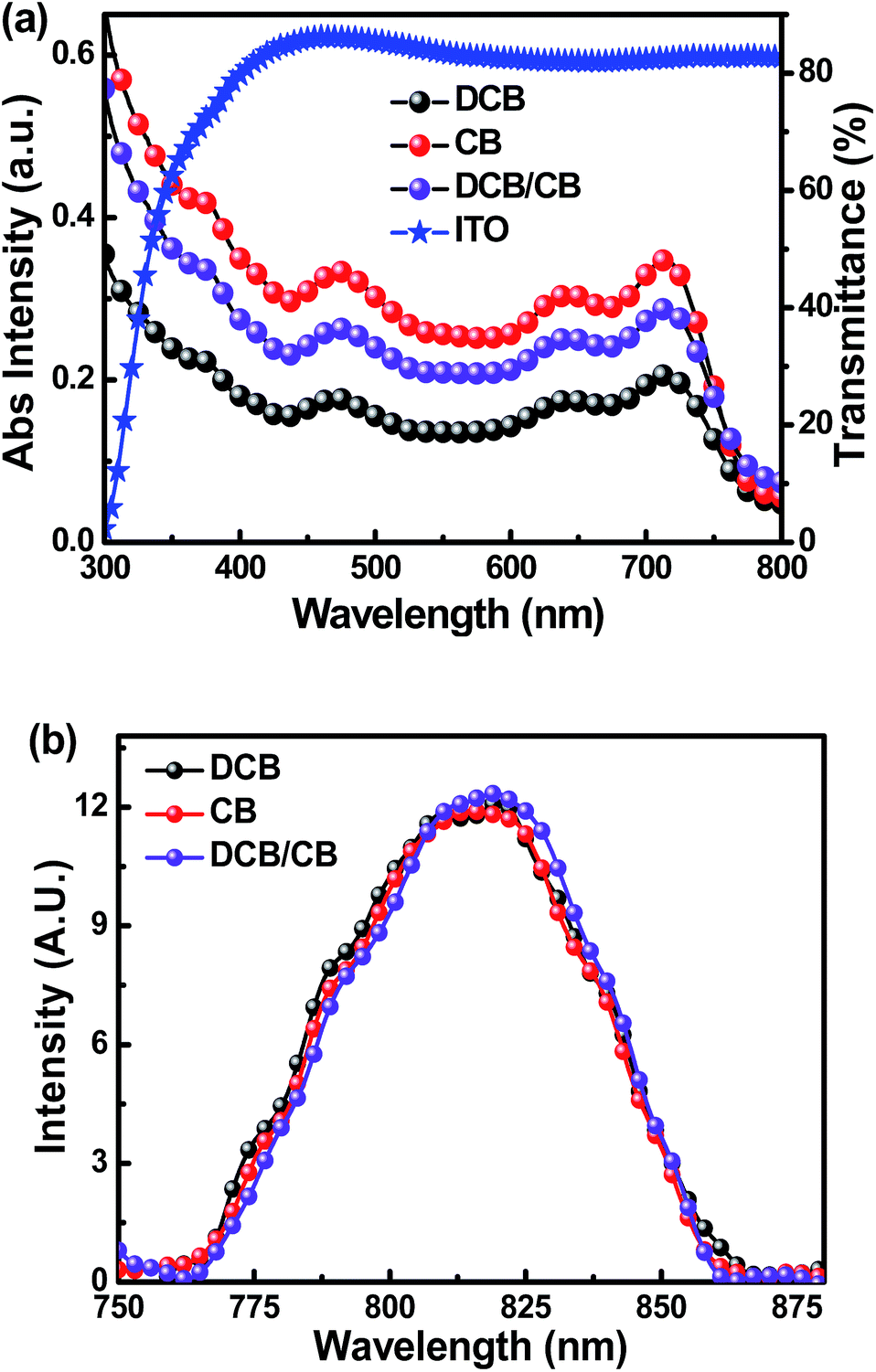 | ||
| Fig. 3 (a) Absorption spectra of PBDTTT-EFT:PC71BM blend films processed by different solvents, the transmittance spectrum of ITO substrate. (b) Emission spectrum of PBDTTT-EFT in different solvents. | ||
In order to further investigate the effect of solvent on the electrical properties of blend films, the dark J–V characteristic curves of all PSCs were measured and are shown in the Fig. S7.† According to the single logarithmic dark current curves of all PSCs, thePSC processed with DCB/CB as solvent have the smallest leakage current density under reverse bias compared with the PSCs processed with DCB or CB as solvent. It is known that the leakage current is determined by the blend films quality and the electrodes/active layer interfaces, which are generally associated with the shunt resistance (Rsh) and series resistance (Rs).38,39 The Rsh strongly depends on the loss of charge carriers through leakage paths including pinholes in the films and charge carrier recombination during transporting through the active layer.40 The relative small Rs indicates a good bi-continuous interpenetrating network for low bulk resistance of active layer and a better active layer/electrode interface for low contact resistance.41 The PSCs processed with DCB/CB as solvent exhibit the largest Rsh and the lowest Rs among all the PSCs, resulting in the optimized FF and PCE.where 2θ is the position of the peak, d is the d-spacing of crystal lattice in a certain direction, FWHM is the full width at half maximum of the peak, D is the crystallite size of blend films.
In order to clarify the effect of solvent on the molecular arrangement of PBDTTT-EFT:PC71BM blend films, X-ray diffraction (XRD) on the blend films was carried out to investigate the structural information such as crystallite size and intermolecular distance, as shown in Fig. 4. The detailed values of the diffraction peak intensity and the d-spacing were calculated according to XRD spectra and are summarized in Table 2. It is apparent that blend films processed with DCB as solvent show lower crystallinity, which is similar with that of the blend films with CB as solvent. The intensity of three pronounced diffraction peaks (2θ = 35.21°, 50.47°, 60.01°) was improved for the blend films processed with DCB/CB as solvent. The detailed information is supplied in Fig. S8.† It indicates that PBDTTT-EFT molecular arrangement may be packed in a more orderly manner in the blend films when processed with DCB/CB as solvent. It is known that DCB has a higher boiling-point (180.4 °C) than that of CB (131.7 °C), resulting in an incomplete crystalline structure due to a larger amount of excess solvent remaining within the active layer.42 The mixed DCB/CB solvent may have a suitable volatilization speed for further PBDTTT-EFT self-organization during solution-to-film transition stage.9 The solvent additive DIO can drive the polymer to self-stack to form the more ordered alignments, while allowing PC71BM to remain in solution longer to avoid excessive fullerene aggregation.43 According to the XRD profiles, the crystallite size of PBDTTT-EFT was decreased from 36.6 nm for DCB as solvent, to 34.7 nm for CB as solvent, and to 27.0 nm for DCB/CB as solvent. The reduced domain size should be beneficial to exciton migration to the D–A interface for charge dissociation, since the diffusion length of the exciton in the organic materials is only small range of 10–20 nm.44,45 The optimized phase separation forming bi-continuous interpenetrating network can effectively enlarge the D–A interfacial area for more efficient exciton separation and charge transportation.
 | ||
| Fig. 4 XRD patterns of the PBDTTT-EFT:PC71BM blend films processed by different solvents. | ||
| Solvent | 2θ (deg) | d (nm) | Intensity | FWHM (deg) | D (nm) |
|---|---|---|---|---|---|
| DCB | 35.220 | 2.546 | 447 | 0.294 | 36.6 |
| CB | 35.221 | 2.552 | 445 | 0.339 | 34.7 |
| DCB/CB | 35.239 | 2.545 | 519 | 0.360 | 27.0 |
In order to further investigate the effect of solvent and solvent additive on the active layer morphology, the morphology and phase images of blend films were measured by using tapping mode atomic force microscopy (AFM), as shown in Fig. 5. The root means square roughness (Rrms) of blend films are 3.07 nm, 2.73 nm and 1.50 nm for the blend films processed with DCB, CB or DCB/CB as solvents and DIO as solvent additive, respectively. The blend films processed with DCB/CB as solvent have the lowest Rrms value compared to the other blend films. This clearly indicates that the DCB/CB solvent could adjust the miscibility between PBDTTT-EFT and PC71BM leading to the more homogeneous films, which agrees with the d-spacing of crystal lattice and crystallite size obtained from XRD profiles. The individual phase images also show an apparent D–A distribution change induced by using different solvent. The morphologic improvement of the blend films processed with DCB/CB as solvent and DIO as solvent additive results in the increase of Jsc and FF, both of which enhance the performance of PSCs. It means that the D–A phase separation and bi-continuous interpenetrating network could be adjusted by using different boiling point solvents.
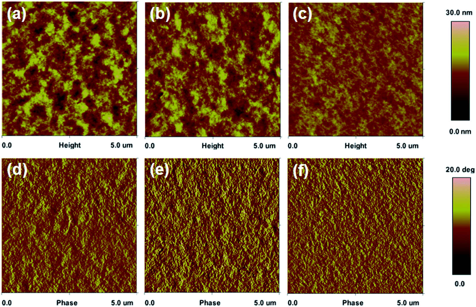 | ||
| Fig. 5 AFM morphology images of PBDTTT-EFT:PC71BM blend films processed with DCB, CB and DCB/CB as solvents (a–c) with additive DIO, the individual phase images (d–f). | ||
In order to finely adjust the morphology of active layers for high performance of PSCs, chloroform (CF) vapor annealing treatment was employed on the blend films processed with DCB/CB as solvent and DIO as solvent additive. It is notable that solvent vapor annealing has attracted more and more attention due to its versatility to the dissolvable conjugated polymers, low cost and preventing narrow band gap polymer degradation.46–48 The J-V characteristic curves of PSCs with different time CF vapor annealing treatment were measured under illumination 100 mW cm−2 AM 1.5G simulated solar light and are shown in Fig. 6a. The key photovoltaic parameters of PSCs with different time CF vapor annealing treatment are listed in the Table 3. It is apparent that the Jsc of PSCs was firstly enhanced and then weakened along with the increase of CF vapor annealing treatment time. The maximum 7.58% PCE of PSCs was obtained for the active layers with 60 s CF vapor annealing treatment, along with a Jsc of 14.88 mA cm−2, a Voc of 0.79 V and FF of 64.5%. For the PSCs with CF vapor annealing treatment more than 3 minutes, the Voc, Jsc and FF values were significantly decreased due to the getting worse morphology of active layer, resulting in the low 4.85% PCE with a 36% decrease compared to the maximum 7.58% PCE. As we know, the morphology of active layer is crucial to the electrical properties of PSCs, especial to the series resistance and shunt resistance. The Rs was decreased from the initial value of 4.9 Ω cm2 to 2.5 Ω cm2 and then increased to 8.3 Ω cm2 along with the increase of CF vapor annealing treatment time. The Rsh was increased from the initial value of 97.2 Ωcm2 to 116.9 Ω cm2 and then decreased to 90.5 Ω cm2, when CF vapor annealing time arrives to 60 s and further prolongs to 3 minutes. It is known that the FF should mainly depend on the Rs and Rsh,43,49,50 the optimized 64.5% FF was obtained when the Rs and Rsh arrives to its minimum and maximum value, respectively. The dark J–V characteristic curves of PSCs with different time solvent vapor annealing treatment are shown in Fig. 6b. The PSCs with 60 s CF vapor annealing treatment show the least amount of current leakage at low and reverse bias, which should be attributed to the distribution of PBDTTT-EFT and PC71BM, especially on the top surface of active layer.
 | ||
| Fig. 6 (a) J–V characteristics curves of PSCs with the active layers under CF solvent annealing for different times under illumination 100 mW cm−2 AM 1.5G simulated solar light. (b) Single logarithmic of J–V characteristics curves of PSCs with the active layers under different CF solvent annealing time. | ||
| Time | Voc (V) | Jsc (mA cm−2) | FF (%) | Best PCE (%) | Ave PCE (%) | Rs (Ω cm2) | Rsh (Ω cm2) |
|---|---|---|---|---|---|---|---|
| a The average PCE was evaluated based on 30 cells. | |||||||
| 0 s | 0.79 | 13.63 | 62.9 | 6.77 | 6.70 ± 0.07 | 4.9 | 97.2 |
| 30 s | 0.79 | 14.74 | 62.9 | 7.32 | 7.22 ± 0.10 | 3.1 | 109.6 |
| 60 s | 0.79 | 14.88 | 64.5 | 7.58 | 7.46 ± 0.12 | 2.5 | 116.9 |
| 90 s | 0.79 | 14.56 | 62.5 | 7.19 | 7.12 ± 0.07 | 3.3 | 107.9 |
| 120 s | 0.79 | 14.17 | 59.0 | 6.61 | 6.56 ± 0.05 | 5.3 | 90.5 |
| 180 s | 0.77 | 12.56 | 58.6 | 5.67 | 5.64 ± 0.03 | 7.06 | 84.11 |
| 360 s | 0.76 | 11.41 | 55.9 | 4.85 | 4.77 ± 0.08 | 8.30 | 70.12 |
The EQE spectra of PSCs with different CF vapor annealing treatment time were measured and are shown in Fig. 7. The EQE values of PSCs from 350 nm to 500 nm were firstly increased and then decreased along with the increase of CF vapor annealing treatment time. The maximum EQE value arrives to 73% at the 360 nm light, which is a relative high reported value. Meanwhile, the EQE values were decreased in the longer wavelength range from 550 nm to 750 nm along with CF vapor annealing treatment time, which corresponds to the absorption range of PBDTTT-EFT. The decreased EQE values in the longer wavelength range should be attributed to the more PBDTTT-EFT aggregation, resulting in the limited exciton dissociation. Xiao et al. also reported that a method to boost the efficiency of PSCs by forming a compositionally graded bulk heterojunction with better donor–acceptor bi continuous connection using a simple solvent-fluxing process.51 Chen et al. reported that the solvent quality in the solvent annealing treatment provides a controllable and versatile method to direct the morphology of a conjugated polymer–fullerence nano-composite for further performance improvement of PSCs. The relative variation of EQE spectra means that the contribution of PBDTTT-EFT and PC71BM on the performance of PSCs was changed by individual molecular distribution induced by CF solvent annealing treatment. In order to further confirm the effect of CF vapor annealing treatment on the morphology of PBDTTT-EFT:PC71BM films, the morphology of blend films with different CF vapor annealing treatment time was investigated by AFM, as shown in Fig. 8.
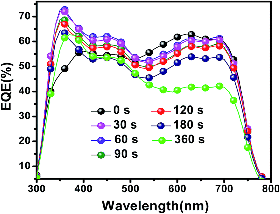 | ||
| Fig. 7 EQE spectra of PSCs with different time CF solvent vapor annealing treatment. | ||
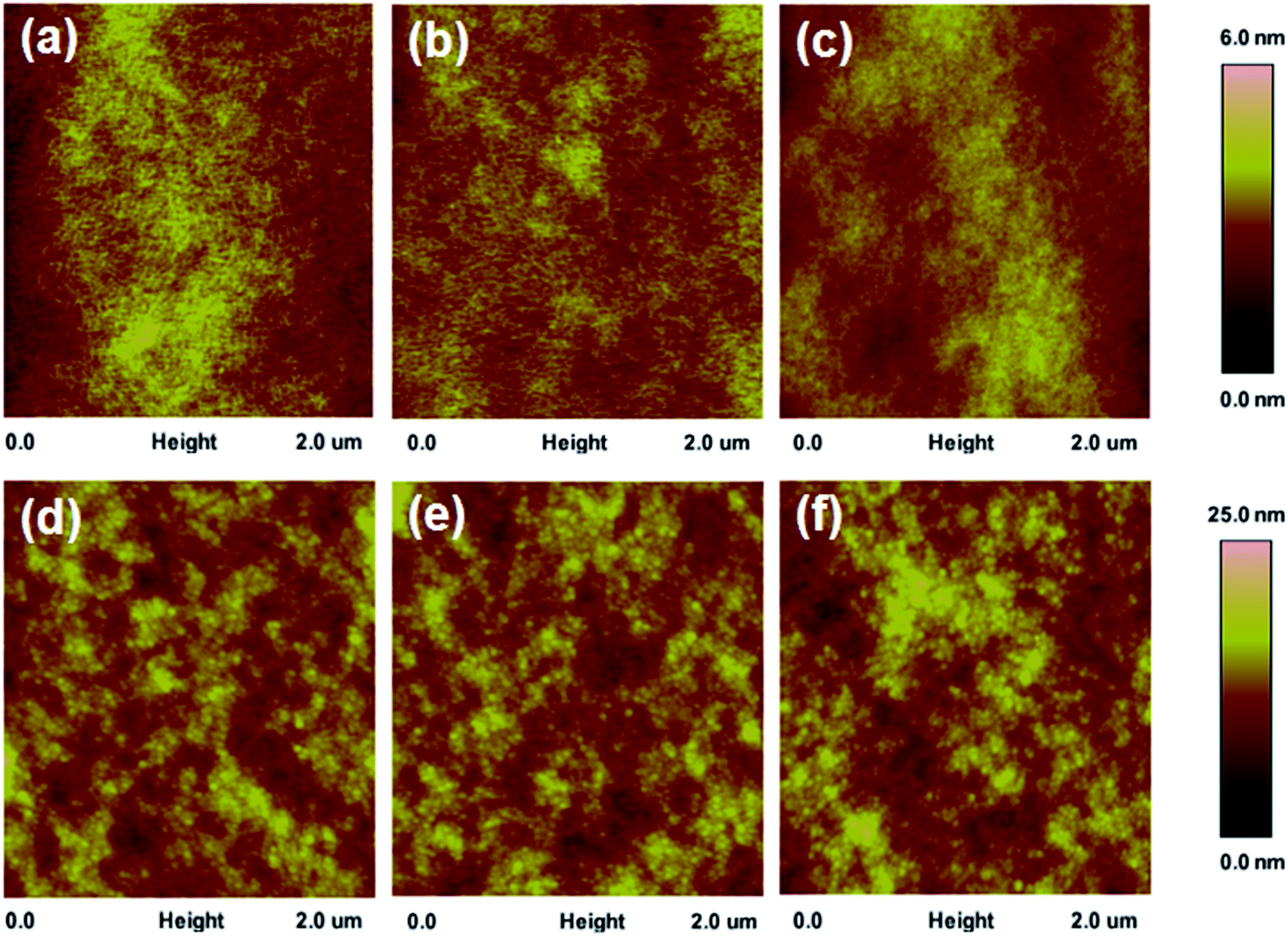 | ||
| Fig. 8 AFM morphology images of PBDTTT-EFT:PC71BM blend films under different time (30 s, 60 s, 90 s, 120 s, 180 s, 360 s) CF vapor annealing treatment. (a) Rrms = 0.58 nm, (b) Rrms = 0.37 nm, (c) Rrms = 0.71 nm, (d) Rrms = 1.88 nm, (e) Rrms = 1.91 nm, (f) Rrms = 2.16 nm. | ||
It is apparent that CF vapor annealing treatment on the PBDTTT-EFT:PC71BM films clearly alters the morphology of blend films along with the increase of CF vapor annealing treatment time, which in turn impacts its ability to act as an active layer for high performance PSCs. The Rrms of blend films was decreased from 1.5 nm of pristine films (as shown in Fig. 5c) to 0.37 nm of films with 60 s CF vapor annealing treatment and then increased to 2.16 nm of films with 6 minutes CF vapor annealing treatment. The PCE of PSCs arrives to the maximum 7.58% for the active layer with the smallest Rrms about 0.37 nm, which also well accords with the phenomenon observed from the effect of solvent on the morphology of active layer and PCE of PSCs. The relative phase images of blend films with different time CF vapor annealing treatment are shown in Fig. S9.† Clearly, the effect of CF solvent annealing treatment on active layers for performance improvement of PSCs was mutually demonstrated by J–V characteristic curves, EQE spectra and AFM images, D–A distribution in the active layer should play the key role in determining the performance of PSCs.
Conclusions
In summary, a series of devices with PBDTTT-EFT:PC71BM as the active layer were fabricated to clarify the positive effect of solvent and solvent vapor annealing treatment on the performance of PSCs. The performance of PSCs should strongly depend on the morphology of active layers, i.e. bi-continuous interpenetrating networks of D–A induced by solvent and solvent vapor treatment. The PSCs processed with DCB/CB as solvent and DIO additive obtains a maximum Jsc and FF, yielding a highest PCE of 7.58%, which is attributed to the fine morphology adjustment for the better exciton dissociation and charge carrier transport in the active layer. These findings indicate that the choice of mixed solvent and solvent vapor annealing treatment provide effective methods to exquisitely control and optimize the morphology of narrow band gap conjugated polymer–fullerene mixtures for high performance PSCs.Experimental details
The indium tin oxide (ITO) glass substrates with sheet resistance 15 Ω □−1 were cleaned by continuously in ultrasonic baths containing in acetone, detergent, de-ionized water and ethanol. Then the cleaned ITO substrates were blow-dried by high pure nitrogen gas and then treated by UV-ozone for 10 minutes to increase the work function of ITO. The solution of PEDOT:PSS (Clevios PVP Al 4083, purchased from H.C. Starck co. Ltd.) was spin-coated onto the cleaned ITO substrates under 5000 rounds per minute (RPM) for 40 s to fabricate the interfacial layers. Then PEDOT:PSS coated ITO glass substrates were annealed in air at 120 °C. After drying for 20 minutes, the substrates were transferred to a nitrogen-filled glove box. The polymer PBDTTT-EFT and [6,6]phenyl-C71-butyric acid methyl ester (PC71BM) (product no. LT-S923, purchased from Luminescence Technology Corp) with a weight ratio of 1:1.5 were dissolved in DCB, CB or DCB/CB (1:1) at a concentration of 25 mg ml−1, and 3% 1,8-diiodooctance (DIO) additive was added into the solutions before the spin-coating process. The blend solutions were stirred with a magnetic stirrer at 60 °C for 12 hours, and then the active layers were fabricated by spin-coating method in a high purity nitrogen filled glove box. The 1 nm LiF interfacial layer and about 100 nm cathode layer Al were deposited by thermal evaporation under 10−4 Pa vacuum conditions, where the thickness was monitored by a quartz crystal microbalance. The active area of about 3.8 mm2 is defined by the vertical overlap of ITO anode and Al cathode. The device architecture is ITO/PEDOT:PSS/PBDTTT-EFT:PC71BM/LiF (1 nm)/Al (100 nm). For the CF vapor annealing treatment, the controlled CF vapor annealing treatment on the blend films processed with DCB/CB mixed solvent was executed in a cuboid box (13 cm in length, 9 cm in height and 10 cm in width), and the PBDTTT-EFT/PC71BM samples were placed at a same height of 6 cm from the CF solvent source. In this process, the CF solvent was added to the cuboid box and heated at 60 °C for 20 min, forming amount of solvent vapor filled in the box. The samples were rapidly placed at the given position in the box and controlled by the amount of treatment time from 30 s to 360 s. The absorption spectra of films were measured with a Shimadzu UV-3101 PC spectrophotometer. The current density–voltage (J–V) characteristics of the PSCs were measured using a Keithley 4200 source measurement unit and an ABET Sun 2000 solar simulator at room temperature in air. Photoluminescence (PL) spectra were measured by a Perkin Elmer LS-55 spectrophotometer. The external quantum efficiency (EQE) spectra were measured by a Zolix Solar Cell Scan 100. The X-ray diffraction (XRD) spectra of the PBDTTT-EFT:PC71BM films drop-cast onto PEDOT:PSS/ITO substrate were obtained by using a Bruker D8 Advance X-ray diffractometer. The morphology of film was investigated with atomic force microscopy (AFM) using a multimode Nanoscope IIIa operated in tapping mode.
Acknowledgements
This work was supported by Fundamental Research Funds for the Central Universities (no. 2014JBZ017); National Natural Science Foundation of China (no. 61377029); Beijing Natural Science Foundation (no. 2122050); Program for New Century Talents in University (NCET-12-0633) and National Natural Foundation of Distinguished Young Scholars of China (no. 61125505). We also thank Yun Zhang for providing help on the synthesis of novel narrow band gap polymer PBDTTT-EFT.Notes and references
- D. D. S. Fung, L. Qiao, W. C. H. Choy, C. Wang, W. E. I. Sha, F. Xie and S. He, J. Mater. Chem., 2011, 21, 16349–16356 RSC.
- Z. C. He, H. B. Wu and Y. Cao, Adv. Mater., 2014, 26, 1006–1024 CrossRef CAS PubMed.
- T. Ameri, T. Heumüller, J. Min, N. Li, G. Matt, U. Scherf and C. J. Brabec, Energy Environ. Sci., 2013, 6, 1796–1801 CAS.
- L. Y. Bian, E. W. Zhu, J. Tang, W. H. Tang and F. J. Zhang, Prog. Polym. Sci., 2012, 37, 1292–1331 CrossRef CAS PubMed.
- Y. Deng, J. Liu, J. Wang, L. Liu, W. Li, H. Tian, X. Zhang, Z. Xie, Y. Geng and F. Wang, Adv. Mater., 2014, 26, 471–476 CrossRef CAS PubMed.
- Y.-W. Su, S.-C. Lan and K.-H. Wei, Mater. Today, 2012, 15, 554–562 CrossRef CAS.
- M. Nam, J. Park, S. W. Kim and K. Lee, J. Mater. Chem. A, 2014, 2, 3978–3985 CAS.
- J. H. Kim, J. Kang, D. Mi, F. Xu, S. H. Jin, H. H. Chun and D. H. Hwang, J. Nanosci. Nanotechnol., 2014, 14, 5187–5191 CrossRef CAS PubMed.
- L. Chang, H. W. A. Lademann, J.-B. Bonekamp, K. Meerholz and A. J. Moulé, Adv. Funct. Mater., 2011, 21, 1779–1787 CrossRef CAS.
- J. Gao, W. Chen, L. Dou, C. C. Chen, W. H. Chang, Y. Liu, G. Li and Y. Yang, Adv. Mater., 2014, 26, 3142–3147 CrossRef CAS PubMed.
- Q. An, F. Zhang, J. Zhang, W. Tang, Z. Wang, L. Li, Z. Xu, F. Teng and Y. Wang, Sol. Energy Mater. Sol. Cells, 2013, 118, 30–35 CrossRef CAS PubMed.
- Q. S. An, F. J. Zhang, L. L. Li, J. Wang, J. Zhang, L. Y. Zhou and W. H. Tang, ACS Appl. Mater. Interfaces, 2014, 6, 6537–6544 CAS.
- F. Z. Wang, Q. Xu, Z. A. Tan, L. J. Li, S. S. Li, X. L. Hou, G. Sun, X. H. Tu, J. H. Hou and Y. F. Li, J. Mater. Chem. A, 2014, 2, 1318–1324 CAS.
- H. Y. Chen, J. H. Hou, S. Q. Zhang, Y. Y. Liang, G. W. Yang, Y. Yang, L. P. Yu, Y. Wu and G. Li, Nat. Photonics, 2009, 3, 649–653 CrossRef CAS.
- L. J. Huo, S. Q. Zhang, X. Guo, F. Xu, Y. F. Li and J. H. Hou, Angew. Chem., Int. Ed., 2011, 50, 9697–9702 CrossRef CAS PubMed.
- J. H. Hou, H. Y. Chen, S. Q. Zhang and Y. Yang, J. Phys. Chem. C, 2009, 113, 21202–21207 CAS.
- S. H. Liao, H. J. Jhuo, Y. S. Cheng and S. A. Chen, Adv. Mater., 2013, 25, 4766–4771 CrossRef CAS PubMed.
- L. Ye, S. Q. Zhang, W. Ma, B. H. Fan, X. Guo, Y. Huang, H. Ade and J. H. Hou, Adv. Mater., 2012, 24, 6335–6341 CrossRef CAS PubMed.
- A. Thomas, A. E. Tom, A. D. Rao, K. A. Varman, K. Ranjith, R. Vinayakan, P. C. Ramamurthy and V. V. Ison, J. Appl. Phys., 2014, 115, 104302 CrossRef PubMed.
- C. G. Wu, C. H. Chiang and H. C. Han, J. Mater. Chem. A, 2014, 2, 5295–5303 CAS.
- S. Venkatesan, N. Adhikari, J. H. Chen, E. C. Ngo, A. Dubey, D. W. Galipeau and Q. Q. Qiao, Nanoscale, 2014, 6, 1011–1019 RSC.
- Z. Xiao, Y. Yuan, B. Yang, J. Vanderslice, J. Chen, O. Dyck, G. Duscher and J. Huang, Adv. Mater., 2014, 3068–3075 CrossRef CAS PubMed.
- R. Dierick, B. Capon, H. Damm, S. Flamee, P. Arickx, E. Bruneel, D. Van Genechten, M. Van Bael, A. Hardy, C. Detavernier, Z. Hens and S. S. Project, J. Mater. Chem. C, 2014, 2, 178–183 RSC.
- B. Y. Huang, J. A. Amonoo, A. Li, X. C. Chen and P. F. Green, J. Phys. Chem. C, 2014, 118, 3968–3975 CAS.
- X. Liu, Q. D. Li, Y. C. Li, X. Gong, S. J. Su and Y. Cao, J. Mater. Chem. A, 2014, 2, 4004–4013 CAS.
- H. Y. Chen, S. H. Lin, J. Y. Sun, C. H. Hsu, S. Lan and C. F. Lin, Nano, 2013, 24, 484009 Search PubMed.
- O. Synooka, K. R. Eberhardt, C. R. Singh, F. Hermann, G. Ecke, B. Ecker, E. von Hauff, G. Gobsch and H. Hoppe, Adv. Energy Mater., 2014, 4, 20130098 Search PubMed.
- Y. Liang, Z. Xu, J. Xia, S. T. Tsai, Y. Wu, G. Li, C. Ray and L. Yu, Adv. Mater., 2010, 22, E135–E138 CrossRef CAS PubMed.
- L. Dou, J. Gao, E. Richard, J. You, C. C. Chen, K. C. Cha, Y. He, G. Li and Y. Yang, J. Am. Chem. Soc., 2012, 134, 10071–10079 CrossRef CAS PubMed.
- J. Gao, W. Chen, L. Dou, C. C. Chen, W. H. Chang, Y. Liu, G. Li and Y. Yang, Adv. Mater., 2014, 26, 3142–3147 CrossRef CAS PubMed.
- Y. Y. Liang, D. Q. Feng, Y. Wu, S. T. Tsai, G. Li, C. Ray and L. P. Yu, J. Am. Chem. Soc., 2009, 131, 7792–7799 CrossRef CAS PubMed.
- Y. Huang, F. Liu, X. Guo, W. Zhang, Y. Gu, J. P. Zhang, C. C. Han, T. P. Russell and J. H. Hou, Adv. Energy Mater., 2013, 3, 930–937 CrossRef CAS.
- M. J. Zhang, X. Guo, W. Ma, S. Q. Zhang, L. J. Huo, H. Ade and J. H. Hou, Adv. Mater., 2014, 26, 2089–2095 CrossRef CAS PubMed.
- Y. S. Liu, C. C. Chen, Z. R. Hong, J. Gao, Y. Yang, H. P. Zhou, L. T. Dou, G. Li and Y. Yang, Sci. Rep., 2013, 3, 3356 Search PubMed.
- S. W. Ko, E. T. Hoke, L. Pandey, S. H. Hong, R. Mondal, C. Risko, Y. P. Yi, R. Noriega, M. D. McGehee, J. L. Bredas, A. Salleo and Z. A. Bao, J. Am. Chem. Soc., 2012, 134, 5222–5232 CrossRef CAS PubMed.
- X. M. Zhao, C. H. Xu, H. T. Wang, F. Chen, W. F. Zhang, Z. Q. Zhao, L. W. Chen and S. F. Yang, ACS Appl. Mater. Interfaces, 2014, 6, 4329–4337 CAS.
- Y. Liu, F. J. Zhang, H. D. Dai, W. H. Tang, Z. X. Wang, J. Wang, A. W. Tang, H. S. Peng, Z. Xu and Y. S. Wang, Sol. Energy Mater. Sol. Cells, 2013, 118, 135–140 CrossRef CAS PubMed.
- V. Gupta, A. K. K. Kyaw, D. H. Wang, S. Chand, G. C. Bazan and A. J. Heeger, Sci. Rep., 2013, 3, 1965 Search PubMed.
- S. W. Heo, K. H. Baek, T. H. Lee, J. Y. Lee and D. K. Moon, Org. Electron., 2013, 14, 1629–1635 CrossRef CAS PubMed.
- S. Das, J. Joslin and T. L. Alford, Sol. Energy Mater. Sol. Cells, 2014, 124, 98–102 CrossRef CAS PubMed.
- A. Turak, T. Aytun and C. W. Ow-Yang, Appl. Phys. Lett., 2012, 100, 253303 CrossRef PubMed.
- L. L. Chang, H. W. A. Lademann, J. B. Bonekamp, K. Meerholz and A. J. Moule, Adv. Funct. Mater., 2011, 21, 1779–1787 CrossRef CAS.
- K. H. Kim, S. C. Gong and H. J. Chang, Thin Solid Films, 2012, 521, 69–72 CrossRef CAS PubMed.
- L. J. A. Koster, O. Stenzel, S. D. Oosterhout, M. M. Wienk, V. Schmidt and R. A. J. Janssen, Adv. Energy Mater., 2013, 3, 615–621 CrossRef CAS.
- S. M. Menke and R. J. Holmes, Energy Environ. Sci., 2014, 7, 499–512 CAS.
- G. Li, Y. Yao, H. Yang, V. Shrotriya, G. Yang and Y. Yang, Adv. Funct. Mater., 2007, 17, 1636–1644 CrossRef CAS.
- H. Y. Lv, X. L. Zhao, W. T. Xu, H. Li, J. Y. Chen and X. N. Yang, Org. Electron., 2013, 14, 1874–1881 CrossRef CAS PubMed.
- H. P. Chen, J. Peet, S. Hu, J. Azoulay, G. Bazan and M. Dadmun, Adv. Funct. Mater., 2014, 24, 140–150 CrossRef CAS.
- S. J. Lee, A. B. Yusoff and J. Jang, RSC Adv., 2014, 4, 20242–20246 RSC.
- M. W. Denhoff and N. Drolet, Sol. Energy Mater. Sol. Cells, 2009, 93, 1499–1506 CrossRef CAS PubMed.
- Z. Xiao, Y. Yuan, B. Yang, J. VanDerslice, J. Chen, O. Dyck, G. Duscher and J. Huang, Adv. Mater., 2014, 26, 3068–3075 CrossRef CAS PubMed.
Footnote |
| † Electronic supplementary information (ESI) available. See DOI: 10.1039/c4ra09417d |
| This journal is © The Royal Society of Chemistry 2014 |