DOI:
10.1039/C4RA09221J
(Paper)
RSC Adv., 2014,
4, 56318-56322
Effects of Ag-ion implantation on the performance of DSSCs with a tri-layer TiO2 film
Received
25th August 2014
, Accepted 9th October 2014
First published on 9th October 2014
Abstract
Tri-layer titania films were doped with Ag ions using MEVVA (metal vapor vacuum arc) ion-implantation, and characterized for photovoltaic performance in dye-sensitized solar cells (DSSCs). The current density was significantly improved with the increasing numbers of implanted Ag-ions. The highest energy-efficiency of 5.85% was achieved for the modified DSSCs by Ag-ion implantation with 1 × 10¹⁶ atom per cm−2. The enhancement effect of Ag-ion implantation on photoelectric performance of the DSSCs contributed toward the decrease in charge-transfer resistance and enhancement of dye adsorption. In addition, the Ag-doping induced an impurity level, which reduces the recombination rate of electrons and positively shifts the conduction band edge of titania to match the LUMO level of the dye.
1. Introduction
Dye-sensitized solar cells (DSSCs) have been extensively studied and are increasingly attractive in the past two decades, due to their low cost, excellent performance, and potential applications for commercialization.1–5 In a typical structure of DSSCs, a mesoporous titania film plays an important role as a medium for dye adsorption and charge transport. Desirable properties of titania films include large surface area, fast charge transport, appropriate band structure to match the LUMO level of dye, and a minimal number of electron–hole recombination centers. However, many studies found that titania films contain lots of surface- and inner-defects, which increase the chance of charge recombination and lower the performance of DSSCs.6 Active researches are being focused on engineering the morphology, charge transport, electronic band structure, and defects of titania films.
Doping titania with metals or nonmetals has been considered the most effective method to tailor the photovoltaic properties of photoanode titania films. Doping Mn+ + Co+, Ta+ and V+ ions was found to induce a positive shift of the conduction band of titania, which improves the driving force of injecting electrons from dye to titania.7–9 For N+, B+ and C+ dopants, the doping states are in the band gap of bulk titania, and influence light absorption and electron transport.10–12 However, most of the doping experiments used chemical methods and the doping processes were carried out before or during the fabrication of titania films.13 Due to the complexity of the chemical reactions, accurate control of experimental conditions and reproducibility is frequently a problem of the chemical doping methods. Physical doping (such as high-energy beam modifications), which are capable of post-processing synthesized titania films for further improvements, were largely neglected and few work was conducted in the researches for doping DSSC electrodes.
Ion implantation technique provides a convenient way to modify physical and chemical properties of materials. However, there are rare reports on enhancement of photovoltaic properties for DSSCs with ion implantation.14 Hou et al. calculated the electronic structure of Ag-implanted titania, the result indicated Ag implantation narrowed the band gap of titania, which enhanced visible light activity and photocatalytic properties of titania.15 But, the photoelectric properties of Ag-implanted titania were not investigated in their work. In this work, we use ion implantation to prepare Ag-ion doped tri-layer titania films for DSSCs, investigate the effects of doping on the photovoltaic properties of a series of Ag-doped cells. This report also contains a theoretical analysis of the doping effect of Ag ions.
2. Experiments section
2.1 Preparation of Ag-ion implanted titania tri-layer films
Three kinds of titania pastes consisting of titania particles of different sizes were screen-printed on a F-doped SnO2 conductive glass (FTO glass) substrate to make the titania tri-layer photoanodes. The titania pastes were prepared following the procedures in ref. 16. A 6 μm thick transparent layer was printed using the paste of titania particles of 20 nm (a type of commercial nanoparticles named P25) on the FTO substrate, forming the bottom layer. This layer was covered by a 6 μm thick layer of mixed paste (made up of pastes of titania particles of 20 nm and 200 nm, in the mass ratio of 6![[thin space (1/6-em)]](https://www.rsc.org/images/entities/char_2009.gif) :4). The top layer is a 2 μm thick scattering layer of paste consisted of titania particles of 200 nm. Before the screen printing, the FTO glass was treated by ultrasonic cleaning in deionized water and alcohol, and immersed in 40 mM TiCl4 aqueous solution at 70 °C for 30 min. After being sintered at 500 °C for 30 min, the tri-layer films were placed in a MEVVA (metal vapor vacuum arc) implanter (see for details of the implanter in ref. 17 and 18). The accelerating voltage was set to a low-energy of 8 kV at a high-vacuum level (<1 × 10⁻³ Pa) at room temperature, to limit possible damage to the films induced by the ions. Variable contents of Ag ions of 1 × 10¹⁵, 2 × 10¹⁵, 4 × 10¹⁵, 6 × 10¹⁵, 1 × 10¹⁶ atom per cm−2 were implanted, and the resultant samples were named Ag100–TiO2, Ag200–TiO2, Ag400–TiO2, Ag600–TiO2, Ag1000–TiO2, respectively. A 3.7 nm ions penetration depth and 10 nm ions projection was calculated by using SRIM software with the condition of implantation energy 8 keV. The Ag-implanted samples were compared with the unimplanted sample to investigate influence of dose on the photoelectric properties of the devices.
:4). The top layer is a 2 μm thick scattering layer of paste consisted of titania particles of 200 nm. Before the screen printing, the FTO glass was treated by ultrasonic cleaning in deionized water and alcohol, and immersed in 40 mM TiCl4 aqueous solution at 70 °C for 30 min. After being sintered at 500 °C for 30 min, the tri-layer films were placed in a MEVVA (metal vapor vacuum arc) implanter (see for details of the implanter in ref. 17 and 18). The accelerating voltage was set to a low-energy of 8 kV at a high-vacuum level (<1 × 10⁻³ Pa) at room temperature, to limit possible damage to the films induced by the ions. Variable contents of Ag ions of 1 × 10¹⁵, 2 × 10¹⁵, 4 × 10¹⁵, 6 × 10¹⁵, 1 × 10¹⁶ atom per cm−2 were implanted, and the resultant samples were named Ag100–TiO2, Ag200–TiO2, Ag400–TiO2, Ag600–TiO2, Ag1000–TiO2, respectively. A 3.7 nm ions penetration depth and 10 nm ions projection was calculated by using SRIM software with the condition of implantation energy 8 keV. The Ag-implanted samples were compared with the unimplanted sample to investigate influence of dose on the photoelectric properties of the devices.
2.2 DSSCs assembly
The Ag-implanted and un-treated samples were dipped into 40 mM TiCl4 solution at 70°C for 30 min, and sintered at 500 °C for 30 min. Then, the samples were cooled to 80–100 °C and immersed immediately in a 0.5 mM dye solution of cis-bis (isothiocyanato) bis (2,2-bipryridyl-4,4′-dicarboxylic acid) ruthenium(II) (N719).19 The procedure of sensitization continued for 24 h at room temperature in the dark to allow for complete adsorption of dye molecules. A platinum paste was screen-printed on another FTO substrate, dried at 100°C for 1 h and annealed at 400 °C for 10 min, for the platinization of the counter-electrode. The dye-coated working-electrode and Pt counter-electrode were assembled into a sandwich type cell. A redox (I−/I3−) electrolyte was injected between the two-electrodes. The cells did not seal up and the active area of the working electrode was 0.25 cm2.
2.3 Characterization
X-ray diffraction (XRD) was performed using a D/Max-2200 X-ray diffractometer with Cu Kα radiation, and the scattering angles (2-theta) are 20–40°. A JSM-6700F cold field emission scanning electronic microscope (FE-SEM) equipped with an energy-dispersive X-ray spectroscopy (EDS) detector was employed for measuring the morphology of the Ag-ion implanted films and un-treated films. Photocurrent–voltage characteristics were measured with a solar light simulator (Oriel, 91160-1000) under intensity of 100 mW cm−2, at AM1.5. The monochromatic incident photon-to-collected electron conversion efficiency (IPCE) spectra were examined by a Qtest Station 2000AD in the range of wavelengths from 200 nm to 800 nm. The electrochemical impedance spectra (EIS) were carried out by an electrochemical workstation CHI660E at a forward bias of 0.75 V, in the frequency range from 1 Hz to 100 kHz.
3. Results and discussion
3.1 Crystal structures and morphology
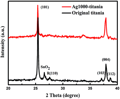
Fig. 1 shows the X-ray diffraction patterns of Ag-ion implanted titania and the untreated titania. The spectra indicate no presence of Ag or Ag compounds in the Ag-doped titania thin films. However, as will be shown later, Ag element mapping clearly evidenced the presence of Ag. The reason may be that the Ag ions were deeply dispersed below the surface of the titania films and the associated electron clouds failed to scatter X-ray coherently to produce a recognizable pattern. The diffraction peak at 2θ = 27.5°, marked as R (110) in Fig. 1, is for the rutile phase and is present only in the diffraction pattern of the untreated titania films. The absence of this peak in the diffraction pattern of Ag1000–titania indicates a phase transformation from rutile to anatase has occurred during the Ag-ion implantation. The phase transition is conducive to electron-transfer because, as we know, electron transport in anatase is faster than in rutile.20 The Ag-ion implantation also influenced the lattice structure of titania. Slight expansions were observed after Ag-ion insertion into titania lattice, e.g. the lattice parameters for the original titania are a = 3.6954 Å, c = 9.3804 Å, while for Ag1000–titania they are a = 3.7716 Å, c = 9.5016 Å.
 |
| | Fig. 1 XRD pattern of original titania and Ag1000–titania. | |
After the ion-implantations, all the films show a metallic luster and gray, in contrast to the white color of the untreated films. The mesoporous morphologies of the original titania and Ag1000–titania were presented in Fig. 2. The tri-layer films are highly uniform and porous, which are expected to enhance dye adsorption and electrolyte penetration. There was no obvious change in the two samples from FE-SEM except the surface of Ag1000–TiO2 showing more flat morphology than that of the original titania films. The phenomenon is well explained by previous researchers.21,22 The inset of Fig. 2 is an element mapping, which exhibits the presence and irregular dispersion of Ag in the titania film. The number of Ag ions in the Ag-doped TiO2 films was too small to be detectable by EDS. The element of Ag was found only in the Ag-ion implanted titania film at dose of 1 × 1016 cm−2.
 |
| | Fig. 2 SEM images of the original (a) and Ag1000–titania films (b). The inset is Ag element mapping with same scale. | |
3.2 Photoelectric properties
The energy conversion efficiency (η) of DSSCs relates to the open circuit (VOC), current density (JSC), fill factor and the intensity of the incident light (PS) as follows:| |
 | (1) |
The J–V characteristics were presented in Fig. 3 for the DSSCs using the untreated titania and Ag-ion implanted titania films under AM1.5 full sunlight, and the photoelectric parameters of all cells were summarized in Table 1. The J–V curves show apparently a beneficial effect of Ag-ion implantation on the photoelectric performance of the photoanodes. With increasing concentrations of Ag-ion implantation, JSC exhibit an obvious trend of increasing. This may be interpreted as follows. The Ag ions act as the centers of recombination in titania films at low doses (below the 1 × 10¹⁵ Ag atom per cm−2), while they play a role of mediator for charge transfer at high doses. The phenomenon is similar to a previous report by Hachiya et al.,23 VOC, which is determined by the difference between the Fermi level of titania and the redox potential of the electrolyte,24 is increased by 52 mV from Ag400–TiO2 to Ag1000–TiO2. It indicated that the Ag-ion doping positively moves the conduction band edge of titania. The DSSC using Ag1000–TiO2 exhibits the highest conversion efficiency (5.85%), in contrast to that of the original cell (4.36%). The poor performance of the original cells may be due to the non-crystalline single-phase of the commercial P25 particles and the unsealed cells during testing in the atmosphere.
 |
| | Fig. 3 (a) J–V curves of DSSCs with original and Ag-ion implanted photoanode. (b) Photovoltaic parameters of DSSCs as a function of the dose of implanted Ag ions. | |
Table 1 The photoelectric parameters of DSSCs with the original and Ag-ion implanted photoanodesa
| Samples |
VOC (V) |
JSC (mA cm−2) |
FF |
η (%) |
Dye adsorption (×10−7 mol cm−2) |
| The desorption of N719 from the TiO2 films by immersing into a 0.1 M NaOH solution (water–ethanol = 1:1 v/v). |
| Ag100–TiO2 |
0.718 |
9.44 |
0.61 |
4.14 |
8.61 |
| Ag200–TiO2 |
0.711 |
10.49 |
0.64 |
4.78 |
8.33 |
| Ag400–TiO2 |
0.7 |
11.24 |
0.59 |
4.61 |
9.05 |
| Ag600–TiO2 |
0.752 |
11.66 |
0.65 |
5.7 |
9.21 |
| Ag1000–TiO2 |
0.724 |
13.04 |
0.62 |
5.85 |
9.57 |
| Unimplanted cells |
0.729 |
9.59 |
0.62 |
4.36 |
7.96 |
The monochromatic incident photon-to-collected electron conversion efficiency (IPCE) corresponds to the external quantum yield of the device and can be defined as follows:
| | |
IPCE = (LHE)(ϕinj)(ηel)
| (2) |
where LHE is the light harvesting efficiency,
ϕinj is the charge injection yield and
ηel is the charge collection efficiency. IPCE spectra of the DSSCs based on the original and Ag-ion implanted tri-layer titania photoanodes are shown in
Fig. 4. The IPCE of the DSSC based on Ag1000–TiO
2 is higher than the original cell, the increase in the IPCE value indicated that dye adsorption of the tri-layer film was enhanced after Ag-ion implantation at 1 × 10
16 atom per cm
−2, which agreed well with the results of Dye adsorption measurements (see
Table 1) and the results of photocurrent–voltage characteristics. As IPCE is related to light harvesting, charge collection and injection, which all depend on the functionality of dye.
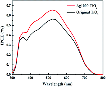 |
| | Fig. 4 IPCE spectra of DSSCs based on the original and Ag-ion implanted tri-layer titania photoanodes. | |
3.3 Electron transport analysis
The spectra of electrical impedance reflect charge-transfer characteristics in DSSCs. The cells are measured under a forward bias voltage of 0.75 V, which is close to the open circuit. The frequency range is 1–100 kHz, and the regions of charge transfer are the cross interfaces of dye-sensitized titania/electrolyte and counter electrode–electrolyte. Electrolyte diffusion is not considered in this work, because it is sensitive only to a much lower frequency range (<1 Hz). Therefore, the equivalent circuit of the DSSCs can be expressed as two RC elements and a series of resistance.25 Nyquist plots for the DSSCs based on the original and Ag-ion implanted TiO2 electrodes are shown in Fig. 5. The plots were fitted to the simulated model of the equivalent circuit (the inset of Fig. 5) by the Z-view software. Rs is series resistance, which contains the ohmic resistance of FTO substrate, the TiO2 layer, the Pt layer and the electrolyte.26 Among them, ohmic resistance of FTO substrate is greatly influenced by Ag-ion implantation. RS for untreated cell is 22.36 Ω, and increased to 56.04 Ω after Ag-ion implantation at 1 × 10¹⁵ atom per cm−2. However, the values of Rs decreased with increasing numbers of implanted Ag ions. It may be due to changes in the FTO substrate's surface, from the sheet resistance of FTO substrate for Ag100–FTO (18.4 Ω □−1), Ag200–FTO (17.2 Ω □−1), Ag600–FTO (15.8 Ω □−1), Ag1000–FTO (15.3 Ω □−1) and the untreated FTO (15 Ω □−1) measured by using the four probe tester. R1 and CPE1 reflect the electron transfer resistance and capacitance at the interface of TiO2/electrolyte, corresponding to the larger semicircle in the plots. R2 and CPE2 express the resistance and capacitance at the interface of counter electrode/electrolyte, represented by the smaller semicircle. The magnitude of R1 and R2 can be estimated from the diameter of the semicircle. The value of R1 is 15.1 Ω, 14.6 Ω, 15.1 Ω and 14.8 Ω for the Ag-doped DSSCs with increasing numbers of implanted Ag ions, respectively, from 1 × 10¹⁵ to 1 × 10¹⁶ atom per cm−2. All the R1 values are lower than that of the original cells (17.6 Ω), indicating that the charge-transfer resistance was reduced mainly due to enhancement of electron transport after the Ag-ion implantation. The electrons lifetime (τeff = (2πf)−1, f is the character frequency) was obtained by EIS fitting with the equivalent circuit model, shown in Fig. 5b. Its value determined the performance of electrons transport and recombination rate in TiO2 films.27 The linear fit show increasing in electrons lifetime with increasing the implanted dose of Ag ions. The larger lifetime of Ag1000–TiO2 indicate that more electrons can transport into outside circuit and less electrons recombined.
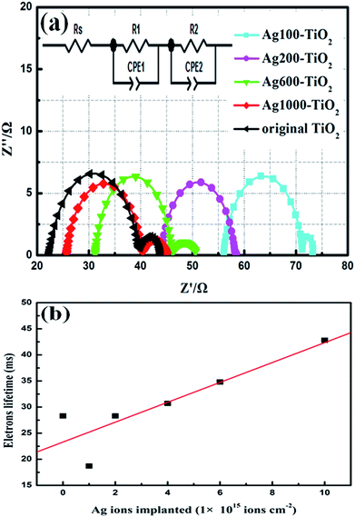 |
| | Fig. 5 (a) Nyquist plots of DSSCs with original and Ag-ion implanted the tri-layered TiO2 film under dark at a forward bias potential voltage 0.75 V. The inset is an equivalent circuit of the cells. (b) Electrons lifetime as a function of the dose of implanted Ag ions, the red line is a linear fit. | |
For further understanding of the effect of Ag-ions on the photoelectric performance, which is related to charge transfer and other photoelectric properties, the band structures of pure TiO2 and Ag-doped TiO2 were computed using first principles calculations based on density functional theory.15 The electronic band structures of pure TiO2 and Ag-doped TiO2 are displayed in Fig. 6. It is observed that the top of value band are positioned at N-point and the bottom of conduction band at Γ-point both in the structure of pure TiO2 and Ag-doped TiO2. This indicates that TiO2 is an indirect-gap material. For the structure of Ag-implanted TiO2, the Ag doping produce the middle states in band gap of TiO2, which is mainly consisted from Ag 4d impurity states. As we know, TiO2 is a wide band gap semiconductor, only response to ultraviolet region. While Ag-doped narrowed the band gap and obviously expanded the light absorption range from UV to visible light (note the different scales in Fig. 6a and b). The extent of modifications to the electronic structure of TiO2 increases with the content of Ag-ion dopant. At low dopant contents, Ag ions in TiO2 films act as “traps” for charge recombination centers, which lead to poor current density as shown in Fig. 3. With increasing dopant content, the doping Ag ions change the electronic structure to enable faster electron injection and transport. There are two “channels” of the conduction band and the Ag 4d states for electrons injection and transport, which reduce the recombination rate of electrons. In addition, Ag-doped positively shift conduction band edge of TiO2 to match the LUMO level of dye, which improve electron injection efficiency from LUMO of excited N719 to conduction band of TiO2. This electronic-structure model explained the increasing JSC of Ag-ion implanted cells with the concentrations of Ag ions, and agreed well with the results of UV-vis absorption measurements.
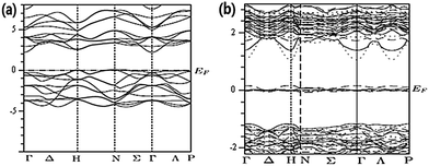 |
| | Fig. 6 Calculated band structure of (a) undoped TiO2 and (b) Ag-doped TiO2. The energy zero represents the Fermi level.15 | |
4. Conclusions
In conclusion, the effects of Ag-ion implantation on the performance of DSSCs were investigated. The Ag ions have tremendous impact on the current density of the devices. At low concentrations (1 × 10¹⁵ atom per cm−2) of Ag-ion implantations, the Ag ions mainly act as recombination centers which decreased current density (JSC) and lowered the performance of DSSCs. At high concentrations of Ag-ion implantations, the implanted Ag ions act as mediators for electron transport, resulting in decrease of charge-transfer resistance and enhancement of dye adsorption. The optimized conversion efficiency (5.85%) and JSC (13.04 mA) were achieved from the cell with Ag1000–TiO2, both values substantially higher than that of the untreated cells.
Acknowledgements
This study is primarily supported by Shanghai Pujiang Program (Grant no. 11PJ1403400) and the National Natural Science Foundation of China (Grant no. 51202139). The authors also acknowledge financial support from the Fundamental Research Funds for Central Universities (Grant no.2012LYB24).
Notes and references
- B. O'Regan and M. Grätzel, Nature, 1991, 353, 737 CrossRef.
- M. Grätzel, Nature, 2001, 414, 338 CrossRef PubMed.
- L. G. Wei, Y. L. Yang, R. Q. Fan, P. Wang, L. Li, J. Yu, B. Yang and W. W. Cao, RSC Adv., 2013, 3, 25908 RSC.
- T. G. Deepak, G. S. Anjusree, S. Thomas, T. A. Arun, S. V. Nair and A. S. Nair, RSC Adv., 2014, 4, 17615 RSC.
- A. E. Shalan, M. M. Rashad, Y. H. Yu, M. Lira-Cantú and M. S. A. Abdel-Mottaleb, Electrochim. Acta, 2013, 89, 469 CrossRef CAS PubMed.
- S. J. Wu and H. W. Han, J. Power Sources, 2008, 182, 119 CrossRef CAS PubMed.
- A. E. Shalan and M. M. Rashad, Appl. Surf. Sci., 2013, 283, 975 CrossRef CAS PubMed.
- J. Liu and H. Yang, Electrochim. Acta, 2010, 56, 396 CrossRef CAS PubMed.
- J. Liu and Y. D. Duan, Appl. Surf. Sci., 2013, 277, 231 CrossRef CAS PubMed.
- S. K. Parka and T. K. Yuna, Appl. Surf. Sci., 2013, 285, 789 CrossRef PubMed.
- H. Tian and L. Hu, J. Mater. Chem., 2011, 21, 863 RSC.
- D. B. Chu, X. M. Yuan and G. X. Qin, J. Nanopart. Res., 2008, 10, 357 CrossRef CAS.
- S. H. Kang and J. Y. Kim, J. Phys. Chem. C, 2007, 111, 9614 CAS.
- G. Dearnaley, Nucl. Instrum. Methods Phys. Res., Sect. B, 1990, 50, 358 CrossRef.
- X. G. Hou, A. D. Liu, M. D. Huang, B. Liao and X. L. Wu, Chin. Phys. Lett., 2009, 26, 077106 CrossRef.
- S. Ito, T. N. Murakami and M. Grätzel, Thin Solid Films, 2008, 516, 4613 CrossRef CAS PubMed.
- T. H. Zhang, X. Y. Wang and H. Liang, Surf. Coat. Technol., 1996, 83, 280 CrossRef.
- A. D. Liu, H. X. Zhang and T. H. Zhang, Surf. Coat. Technol., 2005, 193, 65 CrossRef CAS PubMed.
- M. K. Nazeeruddin, S. M. Zakeeruddin and M. Grätzel, Inorg. Chem., 1999, 38, 6298 CrossRef CAS PubMed.
- V. Thavasi and V. Renugopalakrishnan, Mater. Sci. Eng., R, 2009, 63, 81 CrossRef PubMed.
- P. Romero-Gomez, A. Palmero, F. Yubero, M. Vinnichenko, A. Kolitsch and A. R. Gonzalez-Elipe, Scr. Mater., 2009, 60, 574 CrossRef CAS PubMed.
- P. Romero-Gomez, A. Palmero, T. Ben, J. G. Lozano, S. I. Molina and A. R. González-Elipe, Phys. Rev. B: Condens. Matter Mater. Phys., 2010, 82, 115420 CrossRef.
- A. Hachiya and S. Takata, J. Phys. Chem. C, 2012, 116, 16951–16956 CAS.
- J. Zhang, W. Q. Peng and Z. H. Chen, J. Phys. Chem. C, 2012, 116, 19182 CAS.
- N. Papageorgiou, W. F. Maier and M. Grätzel, J. Electrochem. Soc., 1997, 144, 876 CrossRef CAS PubMed.
- S. M. Zakeeruddin and M. Grätzel, Adv. Funct. Mater., 2009, 19, 1 CrossRef.
- M. Adachi, M. Sakamoto, J. Jiu, Y. Ogata and S. Isoda, J. Phys. Chem. B, 2006, 110, 13872 CrossRef CAS PubMed.
|
| This journal is © The Royal Society of Chemistry 2014 |
Click here to see how this site uses Cookies. View our privacy policy here. 


