Electrochemically etched sharp aluminium probes with nanoporous aluminium oxide coatings: demonstration of addressed DNA delivery

R. Poplausksa, U. Malinovskisa, J. Andzanea, J. Svirkstsab, A. Viksnaab, I. Muiznieksc and D. Erts*a
aInstitute of Chemical Physics, University of Latvia, Riga, Latvia. E-mail: donats.erts@lu.lv
bDepartment of Chemistry, University of Latvia, Riga, Latvia
cDepartment of Biology, University of Latvia, Riga, Latvia

Received 11th August 2014 , Accepted 24th September 2014

First published on 24th September 2014


Abstract

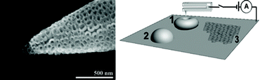
Electrochemical etching of metal wires is widely used to fabricate sharp probes for use in scanning tunnelling microscopy. In this work an electrochemical fabrication method for sharp aluminium probes coated with nanoporous anodised aluminium oxide (AAO) layer is described. The method presented here involves simultaneous anodisation and etching of aluminium wires. The probe apex radius as well as the nanopore length and diameter depend on the etching mode, which could be direct current (DC), alternating current (AC), or pulsed voltage mode (PVM). The probes, coated with a nanoporous AAO layer, were used to demonstrate addressed DNA delivery.


Introduction

Nanoscale probes are widely used in scanning probe microscopy and other areas for material characterisation and surface modification on a local scale.1 Porous tips and nanoscale tip arrays have been proposed for investigation of cell communication problems,2 for drug delivery through the skin,3 and other similar applications. A simple method for obtaining sharp tips for scanning tunnelling microscopes (STM) is electrochemical etching of metal wires.4,5 This process can achieve a tip apex radius of 5 nm.6 Tungsten, platinum–iridium, gold, and silver are the most commonly used materials for nanoprobe fabrication.7 A sharp tip with a nanoporous structure has a significantly increased surface area. This feature enables controlled access and realisation of immobilisation and other processes on the local scale. The combination of electrochemical probe etching (to obtain sharp tips) and electrochemical fabrication of nanoporous coatings by anodising is a promising method for creating sharp structures coated with nanoporous films.

In this paper we present an electrochemical method for fabricating sharp Al probes coated with a nanoporous anodised aluminium oxide (AAO) layer.8 It is one of the most popular and promising materials for template assisted growth of nanostructures9 and for other applications (such as for catalysts, immobilisation enzymes,10 DNA hybridisation and filtration,11,12 sensors,13 and nano-tips14,15). We also demonstrate the application of AAO coated nanoprobes to addressed DNA delivery into the cytoplasm of selected plant cells.

Experimental

The chemicals H3PO4 (analytical grade 85%), HClO4 (70%), H2SO4 (98%) and C2H5OH (96%) were used to prepare the electrolytes. High purity (99.999%) aluminium wires (GoodFellow) with a diameter of 0.25 mm were used as starting material for probe fabrication.

The etching and anodisation was performed at room temperature using three different regimes: alternating current (AC), direct current (DC), and pulse voltage mode (PVM). A homemade two-electrode electrochemical cell and a programmable (±30 V range) voltage source was used to generate rectangular pulses with duration from 10 μs to 1 s, which were applied to the electrodes, the aluminium wire, and a sheet of platinum, which had ∼10 times larger surface area than the aluminium surface. The electrodes were placed inside a 50 mL beaker filled with the electrolyte solution. The immersion depth of the aluminium wire was 2–3 mm. The electrolyte was not stirred during the etching/anodising process in order to reduce the risk of probe apex damage during fabrication. The etching/anodising process was controlled by visual observation under an optical microscope and stopped when the length of the immersed aluminium wire decreased to 0.5–1 mm. After the etching/anodising, the probes were immediately withdrawn from the electrolyte, rinsed with deionised water and allowed to dry naturally at room temperature. The structure of the fabricated probes was investigated by a scanning electron microscope (Hitachi S 4800).

DNA transportation experiments with AAO probes were done using a homebuilt system, which consists of a 3D micromanipulator (SIGNATONE 96MW-MML) placed on an epifluorescent inverted microscope (OLYMPUS IX-71) with a long working distance (10 × 0.3 NA) objective lens. Such a system allowed direct and simultaneous observation of the positioning of the whole probe as well as the DNA sorption/desorption process on the surface of the probe. Detection of the DNA movement into and out of the porous AAO was based on the observation of the colour and intensity of the fluorescence from the whole probe surface. However, this system did not allow precise quantification of the sorbed/desorbed DNA solution. A quartz tuning fork (TF) with an attached probe was mounted on a micromanipulator and used to control the distance between the apex of the probe and the counter electrode/cell surface. The TF oscillation frequency and amplitude were registered and managed using an AFM controller (Nanonis OC4).

Lambda bacteriophage DNA was cut with restriction endonuclease Eco130I (Fermentas), precipitated with isopropanol, dissolved in TE buffer (10 mM TRIS, 1 mM EDTA, pH 8) and labelled with the intercalating dye ethidium bromide (Abmax300 and 360 nm, Emmax 590 nm). The quality and concentration of the DNA achieved from the above process were determined by agarose gel electrophoresis and UV spectrophotometry (Amersham Ultraspec 3110). Single stranded DNA with 6-carboxyfluorescein (Abmax 495 nm, Emmax 520 nm) attached to the 5′ end (5′FAM – GAGATCGGATTGAGGAGGTC, green fluorescent dye) from MWG-Biotech AG was dissolved in TE buffer.

Results and discussion

The widely used method of porous AAO synthesis by anodisation in sulphuric, oxalic, or phosphoric acid aqueous solutions16 was not useful for the fabrication of sharp probes since it resulted in the wire being covered by a nanoporous AAO layer rather than forming a sharp tip. The commonly used acid solutions and anodisation voltages do not yield sufficient aluminium etching speeds. To overcome this problem an attempt was made do perform the probe fabrication in two steps. First, the aluminium wire was etched in a standard electrolyte for electropolishing of aluminium surfaces (HClO4[thin space (1/6-em)]:[thin space (1/6-em)]C2H5OH solution in a 1[thin space (1/6-em)]:[thin space (1/6-em)]5 ratio)16 at a bias of 10 V. A sharp aluminium probe with an apex radius of approximately 200 nm and a smooth surface was obtained as a result of this process (Fig. 1a). Second, the surface of the obtained aluminium probe was anodised under standard conditions (0.3 M H2SO4 at 20 V bias), and the probe apex was covered with a porous AAO layer (Fig. 1b and c). Such experiments resulted in more than 80% defective probes. The porous AAO layer was either damaged or split into several domains (Fig. 1d).
image file: c4ra08509d-f1.tif
Fig. 1 SEM images of (a) Aluminium probe obtained using standard electro polishing conditions (HClO4[thin space (1/6-em)]:[thin space (1/6-em)]C2H5OH solution in a 1[thin space (1/6-em)]:[thin space (1/6-em)]5 ratio at a bias of 10 V); (b) the same probe covered with a nanoporous AAO layer as the result of anodising in standard solution of 0.3 M H2SO4 at 20 V bias; (c) closer view of the porous probe surface; (d) an AAO probe with surface defects.

A significant improvement could be achieved using concentrated acid solutions and rapid switching between the etching and anodising processes. This solution provided a surface anodising process, intensive oxide dissolution, and the formation of the probe apex. Experiments showed that probes coated with an AAO layer could be obtained using electrolytes composed of a mixture of 98% H2SO4, 85% H3PO4, and H2O with a volume ratio in the range of 1[thin space (1/6-em)]:[thin space (1/6-em)]0–2[thin space (1/6-em)]:[thin space (1/6-em)]0.5–4 and a voltage interval of 19–35 V for the DC and 11–18 V at 50 Hz for the AC regimes. Phosphoric acid was added to the etching electrolyte solution on purpose to increase the AAO etching rate. The formation of an AAO layer in the phosphoric acid electrolyte occurs at a bias voltage starting from 80 V.17,18 At our applied voltage of 10–35 V DC it worked just like an AAO dissolving agent. We found that the optimal electrolyte to obtain probes of the best quality is a mixture of sulphuric and phosphoric acids with water in a ratio of 1[thin space (1/6-em)]:[thin space (1/6-em)]1.2[thin space (1/6-em)]:[thin space (1/6-em)]2. Depending on the required probe parameters, which are the probe apex radius, the pore length and the pore diameter, several electrochemical etching modes could be used to obtain the required result.

Direct (DC) and alternating (AC) current etching modes

Use of both direct and alternating current etching regimes resulted in probe pore diameters of 20–60 nm and probe apex radii of 130 nm and larger. The choice of DC or AC regime depends on the required pore length. Use of the DC current mode allows achieving pore lengths that are 10–20 times larger than result from the AC mode, for which pore lengths normally do not exceed 150 nm. The formation of a sharp probe occurs at currents of 100–150 mA. At lower current values Al wire branching was observed instead of probe sharpening. However, currents higher than 150 mA resulted in distortion of the AAO layer. An example of a sharp probe with an apex radius of 130 nm, fabricated by the DC mode, is shown in Fig. 2. The AAO layer grows on the Al surface increasing the electrical resistance and impeding the etching process. To keep the current constant during the process, the applied potential had to be gradually increased from 19 V to a maximum of 35 V in steps of 0.5 V s−1.
image file: c4ra08509d-f2.tif
Fig. 2 SEM images of (a) an aluminium probe with AAO coating fabricated by the DC mode at a constant current of 100 mA and (b) apex of the same probe.

The cross-section structure of the DC-etched probes was investigated to find the pore length and test for the presence of a metal core inside the probe. Fig. 3 shows SEM images of the cross-sections of the DC-etched probes. The probes for the cross-section investigation were randomly selected. In both samples a metal core was present (Fig. 3a and b). The observed pore length can reach 4000 nm at a distance of 50 μm from the probe apex (Fig. 3a) and approx. 1000 nm at a distance of 10 μm from the probe apex (Fig. 3b). The cross-section images also demonstrate that a thick AAO layer formed along the straight planes instead of forming radially along the Al wire surface. Such AAO layer formation results in its splitting between the different planes (Fig. 3a) due to mechanical stress between the straight planes formed on the conical surface.19 The cracked areas at the aluminium surface were covered with a thin, porous AAO layer (Fig. 3c).


image file: c4ra08509d-f3.tif
Fig. 3 SEM images of the cross-sections of the probes. (a) SEM image of the cross-section of the probe showing a metallic Al core at a distance of 50 μm from the apex surrounded by perpendicular cracked, rectangular, nanoporous AAO domains; (b) cross-section of the probe's apex; (c) the probe image showing the crack areas at the aluminium surface covered with a thin porous AAO layer.

The drawback of the DC etching method was aluminium surface passivation, which results in an untimely termination of the probe etching process. The process could be re-established by increasing the applied voltage to the probe. In such cases the etching and anodising process was reinitiated spontaneously and with very high intensity. The average yield of good quality probes fabricated by the DC method was about 10%.

When pore lengths below 150 nm were required, it was preferable to use the AC etching mode, which enables alternating anodising and cathodising processes at the aluminium surface. The cathodising process caused by the negative half-period of the AC bias resulted in intensive etching of the probe surface in addition to the primary etching by phosphoric acid. Cathodising could be explained as a partial etching of an AAO layer previously formed during the positive half-period of the AC voltage cycle as a result of an increase in the concentration of hydrogen ions next to the AAO surface as a result of water hydrolysis:21

 
Al2O3 + 6H+ → 2Al3+ + 3H2O (1)

It was found that a nanoporous layer formed at the probe surface when the applied AC bias was between 11 and 18 V. The best quality probes were obtained at 14–15 V AC bias (Fig. 4a). Probes fabricated in the AC mode had a pronounced conical apex structure. Investigation of the cross-section of randomly chosen probes showed that the nanopore length was approximately 150 nm (Fig. 4b) and apex radii varied in the range of 250–1000 nm.


image file: c4ra08509d-f4.tif
Fig. 4 SEM images of an AAO coated probe with an apex radius of 250 nm (a) the aluminium probe covered with an AAO layer fabricated by the AC regime at 15 V amplitude and 50 Hz frequency; (b) determination of the thickness of the probe's nanoporous AAO layer.

Pulsed voltage mode (PVM)

Pulsed voltage etching mode (PVM) was developed to improve the process control of the probe fabrication process. It allowed production of probes covered with an ultra-thin (50 nm) nanopore layer and improved sharpness. The PVM mode was realised with a programmable voltage source, which applied variable voltage, pulse width, and polarity between the electrodes of the electrochemical cell.

The width of the positive pulse was selected based on the data from the kinetic curve of the electrical current density for the anodising process of planar surfaces in a standard (20 V DC, 0.3 M H2SO4) electrolyte solution20–22 (Fig. 5 inset). This kinetic curve depicts the time intervals during which the bottom AAO barrier layer of the pores (I) and the base of the pores (II) were formed. Region (III) of the curve indicates the process of pore growth and the increase of the coating thickness.


image file: c4ra08509d-f5.tif
Fig. 5 Real time diagram for the PVM mode: the solid line is the electrical current (primary vertical axis), the dashed line is the amplitude of the pulses (secondary vertical axis). Width and amplitude were respectively 0.3 s and 14 V for the positive, and 0.4 s and −10 V for the negative pulses. Inset: kinetic curve of the current density in a standard electrolyte solution for the anodising process of planar surfaces.

For the sharp probe apex formation to occur, the speeds of the anodising and etching processes must be balanced. The width of the positive pulses was controlled in real time to mimic the current changes of the kinetic curve to be equal to the length of region I, which stops at the lowest point of the kinetic curve in the inset of Fig. 5. At that point, the pulse polarity was switched to negative. Switching from positive to negative pulses occurred in the automatic regime if the current remained constant or increased during three successive measurements (the time interval of one measurement was 2.5 ms). If the positive pulses were wider, the kinetic process would move to region II, pores would start to be formed, and the AAO layer would grow in thickness and reduce the speed of the probe apex etching.

The best quality probes were obtained using a mixture of sulphuric and phosphoric acids with water in a 1[thin space (1/6-em)]:[thin space (1/6-em)]1.2[thin space (1/6-em)]:[thin space (1/6-em)]2 ratio as electrolyte and a the positive pulse amplitude between 10 and 25 V. At higher pulse amplitudes intensive side reactions (release of gases) started impeding the formation of the pores. At lower positive pulse amplitudes it was not possible to obtain sharp probe apexes.

The cathodising process occurred during the negative pulse and, similarly to the AC regime, (1) resulted in partial or full dissolution of the AAO barrier layer formed during the time of the previous positive pulse. As can be observed from the current–time curve (Fig. 5), the electrical current during the negative pulse was higher than during the positive pulse of the same value. This observation corresponds to partial etching of the AAO layer during the negative pulse. This process promotes further the probe apex etching reaction. The optimal amplitude and width of the negative pulse were chosen experimentally based on the quality of the obtained probes. The amplitudes of the negative pulses were between 5 and 12 V. The reduction of the current amplitude during the positive pulse after 46 seconds of anodising/etching (Fig. 5) is caused by a decrease of the probe surface and indicates that the probe formation has finished, and the etching/anodising process should be interrupted.

The negative pulse current decrease was accompanied by current fluctuations (Fig. 5) whose nature is not understood yet.

The control of the proportion of negative and positive pulses during etching/anodising process in the PVM mode allowed obtaining sharper probe apexes than in the AC or DC modes. It was possible to obtain probes with apex radii down to 80 nm (Fig. 6).


image file: c4ra08509d-f6.tif
Fig. 6 SEM image of a sharp aluminium probe with an AAO coating obtained in the PVM mode. The duration of positive (+15 V) was 0.3 s and negative (−10 V) respectively 0.4 s. The radius of the tip apex is 80 nm.

DNA addressed delivery to the plant cells using nanoporous AAO probe

For the DNA transition tests, a device based on a quartz tuning fork was constructed (Fig. 7). The DNA molecules have a negative charged phosphate backbone. Therefore, they could be moved inside a liquid if an external electrical field was applied. The bias applied between the probe and the ITO surface electrode (0.1–1.0 V) to accomplish the electrophoretic process did not exceed the water splitting potential (1.25 V at 25 °C)23 in order to avoid the formation of atomic oxygen which could have oxidised DNA molecules. The circuit current limitation was set to 30 nA to prevent intensive chemical reactions in the buffer solution. Prior to the electrophoretic process with the DNA the probes were kept in deionised water for 24 hours to dissolve the anodising acid residues and to remove any air from the pores. Then, the probes were immersed into the TE buffer solution to fill the pores with the solution.
image file: c4ra08509d-f7.tif
Fig. 7 Schematic diagram of the experimental setup for addressed DNA delivery. Position (1): a drop of ethidium-bromide-labelled Eco130I-digested λ bacteriophage DNA solution; position (2): a drop of clean TE buffer solution to which DNA should be transferred; position (3): monolayer of Allium cepa (onion) epidermal cells for addressed DNA delivery demonstration.

A drop of ethidium-bromide-labelled Eco130I-digested λ bacteriophage DNA solution (1 μL, 10 ng μL−1) was deposited on ITO glass. To check the ability of the probe to transfer and deliver the DNA molecules, the probe was immersed into this drop (Fig. 7, position 1). For the DNA electrophoretic sorption, a positive voltage of 0.5 V was applied between the probe and the ITO substrate. Then the nanoporous probe filled with the DNA molecules was withdrawn from the DNA solution drop and moved into the TE buffer solution drop (Fig. 7, position 2) for the DNA desorption process. The DNA sorption and desorption processes were visually detected by observing the colour and intensity of the fluorescence of the probe (Fig. 8).


image file: c4ra08509d-f8.tif
Fig. 8 Process of sorption (a–c) and desorption (d–f) of DNA molecules marked with ethidium bromide to- and from- the pores of a fabricated probe.

The absorption process of the DNA substance could be controlled by varying the sorption time (Fig. 8). At the beginning of the DNA sorption process, the probe fluorescence colour was blue, which corresponds to the AAO fluorescence (Fig. 8a). Thirty seconds after the beginning of the DNA sorption process, the probe fluorescence colour turned to orange (Fig. 8b), and its intensity increased with time (Fig. 8c). The orange colour matched the fluorescence colour of the ethidium-bromide-marked, double-stranded DNA molecules used for this test and established the DNA sorption by the pores of the probe. For the DNA desorption from the pores, the voltage applied between the probe and the ITO substrate was switched from positive to negative of the same magnitude (−0.5 V). Fig. 9d–f illustrate the DNA desorption from the probe when the fluorescence colour changed from orange to blue as the DNA molecules were desorbed from the pores.


image file: c4ra08509d-f9.tif
Fig. 9 Optical images of Allium cepa epidermal cells before (a) and after (b) DNA delivery.

To test the AAO probe's suitability for DNA delivery into plant cells, Allium cepa (onion) epidermal cells were used. 5′-FAM-labelled, single-stranded DNA dissolved in TE buffer solution (DNA concentration 10 μM) was used for the delivery into the A. cepa cells. A freshly prepared A. cepa cell monolayer was placed on a clean ITO slide serving as electrode (Fig. 7, position 3). To prevent drying of the cells, they were continuously moisturised using filter paper strips saturated with buffer solution. For the DNA delivery, the probe was positioned above the chosen cell. The probe position was defined, and the probe was moved to the drop with DNA molecules (Fig. 7, position 1) and immersed into it for 5 minutes for the DNA electrophoretic sorption. After the DNA sorption process was finished, the probe was returned to the previously defined position above the selected cell and lowered until it penetrated the cell. When the plant cell wall and plasma membrane were pierced, the DNA molecules were desorbed from the probe pores into the cytoplasm of the cell.

Fig. 9 illustrates the delivery of the DNA molecules into the cell: Fig. 9a and b show the surface of the cell monolayer respectively before and after the penetration by the probe followed by the DNA desorption. In Fig. 9b the footprint of the probe surrounded by a bright fluorescent spot of delivered DNA molecules is clearly seen, indicating that the DNA molecules were successfully delivered into the cytoplasm of the cell.

Conclusions

A one-stage method for the electrochemical fabrication of sharp nanoporous probes from Al wire was developed. It was determined experimentally that the optimal electrolyte for this method was a mixture of sulphuric and phosphoric acids with water in a 1[thin space (1/6-em)]:[thin space (1/6-em)]1.2[thin space (1/6-em)]:[thin space (1/6-em)]2 ratio. The electrochemical process could be accomplished in the DC, AC, or PVM regimes. The fabricated probes were covered with a nanoporous AAO layer with pore diameters of 20–60 nm. Pore lengths depended on the etching/anodising regime and varied in the range of 150–4000 nm for the DC and AC regimes. Probe apex radii for the same regimes varied in the range of 130–1000 nm. The PVM regime enabled improved control of the probe fabrication and made it possible to obtain probes with apex radii of 80 nm covered with an ultra-thin 50 nm AAO layer. The PVM regime permitted choosing and adjusting the pulsating electric signal that balanced the AAO layer formation process and probe etching speed. In the PVM process the nanoporous AAO layer growth occurred during the positive pulses. During the negative pulses, the previously formed AAO layer was dissolved both electrochemically (cathodising) and chemically (by phosphoric acid). In this process further aluminium surface etching was promoted. As a result, sharper tip apexes in comparison with the AC and DC modes were obtained. Further research is required to standardize the probe fabrication process and to understand the influence of external conditions as temperature, diffusion, and gas release on the rate of the etching/anodising process.

The fabricated probes were used to demonstrate addressed delivery of DNA molecules into the cytoplasm of plant cells. Further development of the experimental setup for the addressed DNA delivery is required to enable accurate dosage of the delivered DNA solution. An improvement of this experimental setup could include direct (detection of fluorescence) and indirect (e.g., quantitative polymerase chain reaction) methods for the precise quantification of sorbed/delivered DNA.

Acknowledgements

This work was supported by ERAF project no. 2010/0251/2DP/2.1.1.1.0/10/APIA/VIAA/096.

Notes and references

  1. T. A. Crowley, B. Daly, M. A. Morris, D. Erts, O. Kazakova, J. J. Boland, B. Wu and J. D. Holmes, J. Mater. Chem., 2005, 15, 2408 RSC.
  2. R. J. Fashing, S. J. Bai, T. Fabian and F. B. Prinz, Microelectron. Eng., 2006, 83, 1638 CrossRef PubMed.
  3. A. Meister, M. Gabi, P. Berh, P. Studer, J. Voros, P. Niedermann, J. Bitterli, J. Polesel-Maris, M. Liley, H. Heinzelmann and T. Zambelli, Nano Lett., 2009, 9, 2501 CrossRef CAS PubMed.
  4. U. J. Quaade and L. Oddershede, Europhys. Lett., 2002, 57, 611 CrossRef CAS.
  5. J. P. Ibe, P. P. Bey, S. L. Brandow, R. A. Brizzolara, N. A. Burnham, D. P. Dilella, K. P. Lee, C. R. K. Marrian and R. J. Colton, J. Vac. Sci. Technol., A, 1990, 8, 3570 CAS.
  6. O. L. Guise, J. W. Ahner, M. C. Jung, P. C. Goughnour and J. T. Yates, Nano Lett., 2002, 2, 191 CrossRef CAS.
  7. J. Abbou, C. Demaille, M. Druet and J. Moiroux, Anal. Chem., 2002, 74, 6355 CrossRef CAS.
  8. H. Masuda and K. Fukuda, Science, 1995, 268, 1466 CAS.
  9. M. Wu, L. Wen, Y. Lei, S. Ostendrop, K. Chein and G. Wilde, Small, 2010, 6, 695 CrossRef CAS PubMed.
  10. S. Park, Y. S. Kim, W. B. Kim and S. Jon, Nano Lett., 2009, 9, 1325 CrossRef CAS PubMed.
  11. I. Vlassiouk, A. Krasnoslobodtsev, S. Smirnov and M. Germann, Langmuir, 2004, 20, 9913 CrossRef CAS PubMed.
  12. P. Takmakov, I. Vlassiouk and S. Smirnov, Analyst, 2006, 131, 1248 RSC.
  13. J. Prikulis, U. Malinovskis, R. Poplausks, I. Apsite, G. Bergs and D. Erts, Plasmonics, 2014, 9, 427 CrossRef CAS.
  14. H. Y. Tsai, H. C. Liu, J. H. Chen and C. C. Yeh, Nanotechnology, 2011, 22, 235301 CrossRef PubMed.
  15. P. C. Chen, S. J. Hsieh, C. C. Chen and J. Zou, J. Nanomater., 2013, 1 DOI:10.1155/2013/164953.
  16. L. Zaraska, G. D. Sulka and M. Jaskula, J. Solid State Electrochem., 2011, 15, 2427 CrossRef CAS.
  17. Q. Wang, G. Wang, X. Han, X. Wang and J. G. Hou, J. Phys. Chem. B, 2005, 109, 23326 CrossRef CAS PubMed.
  18. J. Bao, D. Xu, Q. Zhou, Z. Xu, Y. Feng and Y. Zhou, Chem. Mater., 2002, 14, 4709 CrossRef CAS.
  19. A. Yin, R. S. Guico and J. Xu, Nanotechnology, 2007, 18, 035304 CrossRef PubMed.
  20. I. Pastore, R. Poplausks, I. Apsite, I. Pastare, F. Lombardi and D. Erts, IOP Conf. Ser.: Mater. Sci. Eng., 2011, 23, 1 Search PubMed.
  21. C. K. Chung, R. X. Zhou, T. Y. Liu and W. T. Chang, Nanotechnology, 2009, 20, 055301 CrossRef CAS PubMed.
  22. U. Malinovskis, R. Popļausks, I. Apsite, R. Meija, J. Prikulis, F. Lombardi and D. Erts, J. Phys. Chem. C, 2014, 118, 8685 CAS.
  23. L. Pauling, General Chemistry, ed. W. H. Freeman, San Francisco, 3rd edn, 1970, pp. 517–519 Search PubMed.

This journal is © The Royal Society of Chemistry 2014
Click here to see how this site uses Cookies. View our privacy policy here.