Electrospun anatase TiO2 nanorods for flexible optoelectronic devices

Shuai Chen ab, Miao Yuac, Wen-Peng Han*ab, Xu Yanab, Yi-Chen Liub, Jun-Cheng Zhangab, Hong-Di Zhangab, Gui-Feng Yuab and Yun-Ze Long*abd
aCollaborative Innovation Center for Low-Dimensional Nanomaterials and Optoelectronic Devices, Qingdao University, Qingdao 266071, P. R. China. E-mail: yunze.long@163.com; han_wenpeng@163.com
bCollege of Physics, Qingdao University, Qingdao 266071, P. R. China
cDepartment of Mechanical Engineering, Columbia University, New York, New York 10027, USA
dCollaborative Innovation Center for Marine Biomass Fibers, Materials and Textiles of Shandong Province, State Key Laboratory Cultivation Base of New Fiber Materials and Modern Textile, Qingdao University, Qingdao 266071, P. R. China

Received 1st August 2014 , Accepted 10th September 2014

First published on 10th September 2014


Abstract

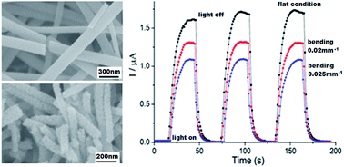
Titanium dioxide (TiO2) nanorods with anatase phase were successfully fabricated by electrospinning and followed calcination. The TiO2 nanorods were characterized by scanning electron microscopy (SEM), X-ray diffraction (XRD), energy dispersive X-ray spectroscopy (EDS) and UV-visible spectroscopy. The diameter of the TiO2 nanorods was about 60–150 nm and the length was 200 nm–2 μm. Electrical properties under bending were investigated by fixing the device to a curved surface with different curvatures, and the device showed a fast and stable resistance response to curvature changing. Photoelectric properties were studied by irradiation with different light intensities. The device exhibited a short response time (∼10 s) and a high sensitivity (∼103) which increased with the light intensity increasing. These results indicate that electrospun anatase TiO2 nanorods have potential applications in flexible photodetectors and solar cells.


1. Introduction

Electrospinning has been recognized as a versatile and efficient method for fabrication of ultrafine fibers from a wide range of materials including organic polymers, semiconductor ceramics, biomacromolecules and even metals with nanometer-to-micrometer size diameters.1,2 Up to now, many complex architectures such as hollow fibers and core–shell fibers have been produced by special electrospinning methods such as coaxial electrospinning.3–5 Besides, it has been achieved to produce single and ordered arrangements of fibers through the optimization of electrospinning conditions.6,7 According to reports, electrospun fibers have many potential applications such as filtration, energy conversion, field-effect transistor, photoelectric devices, chemical sensors, etc.8,9 As the study of electrospun nanofibers continues and the technology tends to mature, researchers now pay much attention to the mass production of electrospun nanofibers in industry, which is a revolutionary progress for their production and applications.10

Recently, the research of flexible devices based on inorganic nanomaterials has attracted much attention due to their fascinating properties such as softness, flexibility, shock resistance and transparency, which is looking forward to the potential applications in paper displays, wearable devices, photodetectors, energy-storage devices and electronic skin field, etc.11 For example, Shen and coworkers have reported high performance p-type Cd3P2,12 Zn3As2[thin space (1/6-em)]13 nanowire photodetectors built on elastic polymer substrate with excellent flexibility and high stability of photoresponse in a broad spectral range. According to these studies, though many semiconductor nanomaterials show excellent optical and electrical properties, their mechanical properties need to be further improved to expand their applications in flexible/stretchable optoelectronic devices.

Titanium dioxide (TiO2) is well known for the potential wide applications such as chemical sensors,14,15 photo catalyst,16 lithium batteries17 and solar cells.18,19 And due to its stability, low cost and environmental protection, TiO2 is also regarded as one of the ideal photochemical materials. For the recent years, air pollution problem caused by PM2.5 suspended particulate has become serious especially in China, TiO2 can play a remarkable role to control the dust concentration to protect the environment because of the self-cleaning and anti-fogging functions. Particularly, one-dimension (1D) TiO2 nanostructures (e.g., nanotubes,20 nanorods,21 nanofibers22 and nanowires23) usually exhibit a more excellent performance due to wide bandgap (Eg = 3.2 eV) and larger specific surface area. For instance, the porous fibrous structure can provide abundant surfactivity sites for effective photocatalysis.24–28 In addition, as we know, synthetic methods have strong influences on optical, electronic and chemical properties of 1D TiO2 nanostructures. So, many different synthetic approaches have been investigated, such as hydrothermal method,29 template growth,30 chemical vapor deposition,31 thermal evaporation32 and electrospinning.33 Compared with other techniques, electrospinning has been considered as a convenient and efficient technique to produce organic, inorganic and composite ultrathin fibers. In the process of electrospinning, the continuity and morphology such as diameter, alignment, nanotubes and coaxial nanostructures of TiO2 could be controlled primely by adjusting the conditions of electrospinning.34,35 However, there are still many challenges need to be solved and further studied such as control of crystalline phases (rutile, anatase and brookite), exploration of flexibility devices and enhancement of photoelectricity under UV-irradiation.

In this work, TiO2 nanorods with anatase phase have been fabricated successfully through electrospinning. The diameters of TiO2 nanorods were ranging from 60 nm to 150 nm and lengths were in the range of 200 nm to 2 μm after calcination under 500 °C for 1 h. In addition, the mechanical and optical properties were also investigated and the results demonstrated the device could be used as the flexible devices and photodetector devices.

2. Experimental

2.1 Fabrication of precursor nanofibers

Firstly, 0.6 g PVP was added into the mixed solvent which containing 8.16 g ethanol, 4.2 g acetic acid and 6.0 g butyl titanate. After magnetic stirring for 2 hours, the mixed solvent becomes uniform and transparent. Then, 4.0 g of the solution was loaded into a 10.0 ml disposable plastic syringe with stainless steel needle which connected to a high-voltage power supply (Tianjin Dongwen, China). A silicon wafer was chose as collector and the distance between the syringe needle and collector was adjusted to 15 cm. A voltage of 20 kV was applied for electrospinning and in the process of electrospinning, the solvent volatilized and butyl titanate/PVP composite nanofibers were deposited on the silicon wafer.

2.2 Calcination under 500 °C to remove PVP

In order to obtain pure crystalline TiO2 nanorods, the obtained precursor nanofibers were calcined under 500 °C for 2.0 h in a muffle furnace (Longkou Electric Furnace Factory, China). Then, the furnace was cooled down to room temperature naturally and the pure crystalline TiO2 nanorods were fabricated.

2.3 Assembly of the TiO2 nanorods devices

For investigating the mechanical and UV photoelectric property of the TiO2 nanorods, the electrode was assembled as follows: firstly, a piece of TiO2 nanorods membrane was placed on a plastic sheet, then coated by silver paste on the both ends of the membrane, and each end was linked with a copper conductive wire. With 30 minutes aeration–drying, polydimethylsiloxane (PDMS) was dropped upon the surface of the TiO2 nanorods membrane to encapsulate so as to be moistureproof. Finally, the device was put into the vacuum drying chamber under 80 °C for 2 h.

2.4 Characterization of TiO2 nanorods

The TiO2 nanorods were characterized by a scanning electron microscope (SEM, FEI DB235 Dual-Beam (FIB/SEM) System), an X-ray diffraction (XRD, Rigaku D/max-2400) diffractometer, and a TU-1901 dual-beam UV-visible spectrophotometer, energy dispersive X-ray spectroscopy (EDS, Hitachi S4800). The electrode was placed in an illumination chamber which was illuminated with various light intensities through adjusting the supplied light power. The light intensity was measured by an UV radiometer (UVATA-UE500, Shanghai). A 50 W xenon lamp (PLS-SXE300UV, Beijing Perfectlight Technology Co.) was used as the light source with the constant distance of 20 cm between lamp and sample. All the photoelectronic measurements for the TiO2 devices were carried out at room temperature in air.

3. Results and discussion

3.1 Morphological and structural properties

Fig. 1 shows the SEM images of the as-obtained precursor and pure TiO2 nanofibers by electrospinning. It's obvious that the precursor nanofibers are very long and the fiber surface is very smooth (Fig. 1a), and their diameters range from 100 nm to 250 nm. After calcination under 500 °C for 1 h, the nanofibers' surface becomes very rough, and the fibers become very short with length ranging from 200 nm to several micrometers. Comparing with the precursor fibers, the diameters of the pure TiO2 nanorods also decrease to 60–150 nm as a result of the removal of organic component PVP and crystallization of TiO2 during calcination.
image file: c4ra07943d-f1.tif
Fig. 1 SEM images of TiO2 nanostructures: (a) butyl titanate/PVP precursor nanofibers; (b–d) different resolutions of pure TiO2 nanorods after calcination under 500 °C for 1 h.

The elemental analysis of TiO2 nanorods was investigated by EDS analysis. As shown in Fig. 2, the sample contains Ti and O elements with theoretical atomic ratio of 1[thin space (1/6-em)]:[thin space (1/6-em)]2. Here, it is noted that a small quantity of element Au was detected because a very thin layer of Au film was deposited onto the sample before AEM imaging. Except Au, no other peak related to impurity was detected in the EDS spectrum, indicating that the sample is free of impurity.


image file: c4ra07943d-f2.tif
Fig. 2 EDS spectrum of pure TiO2 nanorods.

The crystal structure of the TiO2 nanorods after calcination in air at 500 °C for 1 h was investigated by XRD technology. All the diffraction peaks of the XRD pattern as shown in Fig. 3 can be clearly indexed to the anatase phase of TiO2 (JCPDS no. 89-4921). The highest intensity diffraction peak at 2θ = 25.36° is representative of the (101) plane diffraction in the anatase phase of TiO2. Other crystalline phases like brookite and rutile phase diffraction peak have not been detected, demonstrating that the TiO2 of anatase phase is in high purity without any secondary crystalline phase.


image file: c4ra07943d-f3.tif
Fig. 3 XRD pattern of pure TiO2 nanorods.

It's important to confirm the band gap of TiO2 nanorods because that the optical and electrical properties of TiO2 are closely related to the electronic band gap which is affected by the size, shape, impurities, surface charges, and phase transitions, etc.36,37 Fig. 4 shows absorption spectrum of TiO2 nanorods under the UV-visible wavelength region. The band gap energy of the TiO2 nanorods could be obtained to be about 3.2 eV (385 nm in Fig. 4) by extrapolating the linear portion of the plot to the wavelength axis. This value is consistent with the band gap of bulk anatase TiO2 (3.2 eV) by previous reports.38,39


image file: c4ra07943d-f4.tif
Fig. 4 UV-visible absorption spectrum of the TiO2 nanorods.

3.2 Optoelectronic properties of flexible TiO2 devices

The flexible devices of TiO2 nanorods were assembled as shown in Fig. 5a. Polydimethylsiloxane (PDMS) adhesive was a layer of organic polymer which was transparent with a lower Young's modulus leading to a structural flexibility. Due to the coverage of PDMS layer, TiO2 nanorods were encapsulated inside the sheet and could be curled to measure their electrical and optical properties.
image file: c4ra07943d-f5.tif
Fig. 5 Electrical measurements of electrospun TiO2 nanorods device under bending: (a) schematic illustration for the device structure. (b) Schematic illustration for electrical measurement under bending. (c) Sensitivity of TiO2 nanorods under different curvatures. (d) Cyclic response curves under the same curvature (σ = 0.067 mm−1 and the applied voltage was 5.0 V).

As shown in Fig. 5b, the device was fixed on a round object and got a curvature, equaling to get a tension. When fixed on the objects with different diameters, the curvatures and tension values were different from each other. We selected eleven diameters including 50 mm, 45 mm, 40 mm, 35 mm, 30 mm, 25 mm, 20 mm, 15 mm, 13 mm, 10 mm, 7 mm as the variable (the curvature is defined as σ = 1/diameter), and detected the current changes in order to investigate the resistance changes (ΔR/R), as shown in Fig. 5c. The electrical resistance of the TiO2 nanorod device increased with the curvature increasing. For example, the resistance increased to 5–6 times compared with the original value when the curvature was 0.14 mm−1. Due to the inexistence of piezoelectric effect of TiO2, there must be some other reasons which lead to such a large relative change in resistance. In our opinions, the length (L) of the nanorod device may increase and the cross-sectional area (S) may decrease during the bending process. According to the calculation equation of electrical resistance (R = ρL/S), these two trends could result in the increase of the device's resistance. Moreover, when the device was bending, some nanorods may become loosened or fractured, which would increase the conduction distance/barrier of charge carriers and thus decreased the electrical conductivity apparently. From Fig. 5d, we could observe that the resistance increased as soon as the sample got a tension and could recover to the original state immediately when the device returned to a flat position. Additionally, the resistance could drop to the same value nearly in each cycle with the same strain and could fully recover to the original state under flat condition. The results indicate that the resultant TiO2 nanorod sensor exhibits high reproducibility and good stability, is a promising candidate for applications in flexible electronics.

Optoelectronic properties of the nanorod device were also measured by illuminating under a xenon lamp which radiates a wavelength region from 200 to 2500 nm, the current changes could reflect the response to illumination. Under dark condition, the current showed an inconspicuous increase with the increase of voltage. However, when the electrode was exposed under the lamp with light power of 1 mW, the current became increased obviously. The band gap of as-obtained TiO2 nanorods have been calculated to 3.2 eV, so the photon of wavelength region less than 385 nm which the energy is higher than the band gap could be absorbed sufficiently to excite electrons directly from the valence band to the conduction band. As shown in the inset of Fig. 6a, with the increase of the light power, the current increased greater because larger numbers of photons with enough energy could lead to a higher carrier concentration according to Stoletov's law. When the light power reached to 10.24 mW, the photocurrent increased from initial current (background current under bias of 5.0 V) 2.04 nA to 1.74 μA and tended to be saturation with a sensitivity (defined as Imax/I0) as high as 103. From Fig. 6b, we could observe that the TiO2 nanorod devices showed a good cyclicity and reversibility after repeated exposure to illumination (light power was 10.24 mW) with a fast response and recovery speed of ∼10 s.


image file: c4ra07943d-f6.tif
Fig. 6 Optoelectronic properties of electrospun TiO2 nanorods device. (a) IV characteristic curves under dark condition and light illumination. Inset: photoresponse curve under illumination with different light powers (the applied voltage was 5.0 V). (b) Photoresponse curves of TiO2 nanorods under different curvatures (the light power of light illumination was 10.24 mW and the applied voltage was 5.0 V).

In the condition of bending, the photocurrent had a little decrease compared with the current in the flat condition. However, the conductivity had a big improvement towards dark condition. When σ = 0.02 mm−1, the photocurrent increased to 1.31 μA and when σ = 0.025 mm−1, the photocurrent increased to 1.09 μA. The curves showed that bending the sample would block the transport of carriers and the influence of bending deformation was weak relatively towards dark condition (Fig. 5c). When σ = 0.02 mm−1, the resistance changes (ΔR/R) reached to 33% (R is the original resistance under flat condition) and when σ = 0.025 mm−1, it reached to 60%. The results indicate that the TiO2 nanorod devices possess a potential application as a flexible photodetector and solar cells.

Compared to brookite and rutile phase, TiO2 with anatase phase always have a remarkable performance of the photoelectric conversion and photocatalytic activity. However, phase structure is not the only factor which affects its activity. It's also important to control the morphology (e.g., porosity, specific surface and size distribution), crystalline, and surface structure to make sure better device performance. There have been lots attempts to improve the photocatalytic performance of TiO2 nanomaterials under UV light and to extend the light absorption and conversion capacity into the visible light for getting higher solar-energy conversion efficiency. Such studies on flexible TiO2 nanorods via electrospinning are now in progress.

4. Conclusions

TiO2 nanorods with anatase phase were successfully fabricated by electrospinning and followed calcination. From the SEM images, we could observe the nanorods with length ranging from 200 nm to 2 μm and the diameter ranging from 60 nm to 150 nm. We have investigated the mechanical properties of electrospun TiO2 nanorods and found the TiO2 nanorods had a high sensitivity and reproducibility when the sample got a curvature. The results indicate that the as-obtained flexible sensor is a promising candidate for applications in flexible electronics. We also studied the photoresponse properties of the TiO2 nanorods under xenon lamp's illumination and found that the photocurrent became increased with a high sensitivity of 103 when exposed under light with the power of 10.24 mW. The above results exhibited that the electrospun TiO2 nanorods could be applied as a flexible photodetector and solar cells.

Acknowledgements

This work was supported by National Natural Science Foundation of China (51373082), Natural Science Foundation of Shandong Province for Distinguished Young Scholars (JQ201103), Taishan Scholars Program of Shandong Province, China (ts20120528) and National Key Basic Research Development Program of China (973 special preliminary study plan, 2012CB722705), Shandong Provincial Natural Science Foundation, China (ZR2013EMQ003) and Program of Science and Technology in Qingdao City (13-1-4-195-jch).

Notes and references

  1. D. H. Reneker, A. L. Yarin, H. Fong and S. Koombhongse, J. Appl. Phys., 2000, 87, 4531 CrossRef CAS PubMed .
  2. K. H. Lee, Y. H. Kim, M. S. Khil, Y. M. La and D. R. Lee, Polymer, 2003, 44, 1287 CrossRef CAS .
  3. D. Li and Y. Xia, Nano Lett., 2003, 3(4), 555–560 CrossRef CAS .
  4. S. Zhan, D. Chen, X. Jiao and C. Tao, J. Phys. Chem. B, 2006, 110(23), 11199–11204 CrossRef CAS PubMed .
  5. Z. Sun, E. Zussman, A. L. Yarin, J. H. Wendorff and A. Greiner, Adv. Mater., 2003, 15(22), 1929–1932 CrossRef CAS .
  6. P. Katta, M. Alessandro, R. D. Ramsier and G. G. Chase, Nano Lett., 2004, 4, 2215 CrossRef CAS .
  7. L. S. Carnell, E. J. Siochi, N. M. Holloway, R. M. Stephens, C. Rhim, L. E. Niklason and R. L. Clark, Macromolecules, 2008, 41, 5345 CrossRef CAS .
  8. N. J. Pinto, A. T. Johnson, C. H. Mueller, N. Theofylaktos, D. C. Robinson and F. A. Miranda, Appl. Phys. Lett., 2003, 83, 4244–4246 CrossRef CAS PubMed .
  9. H. Q. Liu, J. Kameoka, D. A. Czaplewski and H. G. Craighead, Nano Lett., 2004, 4, 671–675 CrossRef CAS .
  10. L. Persano, A. Camposeo, C. Tekmen and D. Pisignano, Macromol. Mater. Eng., 2013, 298(5), 504–520 CrossRef CAS .
  11. B. Sun, Y. Z. Long, Z. J. Chen, S. L. Liu, H. D. Zhang, J. C. Zhang and W. P. Han, J. Mater. Chem. C, 2014, 2, 1209–1219 RSC .
  12. G. Chen, B. Liang, X. Liu, Z. Liu, G. Yu, X. Xie, T. Luo, D. Chen, M. Zhu, G. Shen and Z. Fan, ACS Nano, 2014, 8, 787–796 CrossRef CAS PubMed .
  13. G. Chen, Z. Liu, B. Liang, G. Yu, Z. Xie, H. Huang, B. Liu, X. Wang, D. Chen, M. Q. Zhu and G. Shen, Adv. Funct. Mater., 2013, 23, 2681 CrossRef CAS .
  14. W.-T. Moon, K.-S. Lee, Y.-K. Jun, H.-S. Kim and S.-H. Hong, Sens. Actuators, B, 2006, 115, 123 CrossRef CAS PubMed .
  15. A. M. More, J. L. Gunjakar and C. D. Lokhande, Sens. Actuators, B, 2008, 129, 671 CrossRef CAS PubMed .
  16. A. Fujishima and K. Honda, Nature, 1972, 238, 37–38 CrossRef CAS .
  17. M. Wagemaker, R. V. D. Krol, A. P. M. Kentgens, A. A. V. Well and F. M. Mulder, J. Am. Chem. Soc., 2001, 123, 11454 CrossRef CAS PubMed .
  18. H. S. Shim, S. I. Na, S. H. Nam, H. J. Ahn, H. J. Kim, D. Y. Kim and W. B. Kim, Appl. Phys. Lett., 2008, 92, 183107 CrossRef PubMed .
  19. Q. Tai, X. Zhao and F. Yan, J. Mater. Chem., 2010, 20, 7366–7371 RSC .
  20. J. Qiu, W. Yu, X. Gao and X. Li, Nanotechnology, 2006, 17, 4695–4698 CrossRef CAS PubMed .
  21. L. Miao, S. Tanemura, S. Toh, K. Kaneko and M. Tanemura, J. Cryst. Growth, 2004, 264, 246–252 CrossRef CAS PubMed .
  22. E. Formo, E. Lee, D. Campbell and Y. Xia, Nano Lett., 2008, 8, 668–672 CrossRef CAS PubMed .
  23. Y. X. Zhang, G. H. Li, Y. X. Jin, Y. Zhang, J. Zhang and L. D. Zhang, Chem. Phys. Lett., 2002, 365, 300–304 CrossRef CAS .
  24. W. K. Chang, F. J. Xu, X. Y. Mu, L. L. Ji, G. P. Ma and J. Nie, Mater. Res. Bull., 2013, 48, 2661–2668 CrossRef CAS PubMed .
  25. M. E. Simonsen, H. Jensen, Z. Li and E. G. Søgaard, J. Photochem. Photobiol., A, 2008, 200, 192–200 CrossRef CAS PubMed .
  26. J. Yu, M. Zhou, B. Cheng, H. Yu and X. Zhao, J. Mol. Catal. A: Chem., 2005, 227, 75–80 CrossRef CAS PubMed .
  27. Q. Zhang, A. K. Chakraborty and W. I. Lee, J. Phys. Chem. Solids, 2008, 69, 1450–1453 CrossRef CAS PubMed .
  28. R. K. Wahi, W. W. Yu, Y. Liu, M. L. Mejia, J. C. Falkner, W. Nolte and V. L. Colvin, J. Mol. Catal. A: Chem., 2005, 242, 48–56 CrossRef CAS PubMed .
  29. B. D. Yao, Y. F. Chan, X. Y. Zhang, W. F. Zhang, Z. Y. Yang and N. Wang, Appl. Phys. Lett., 2003, 82(2), 281–283 CrossRef CAS PubMed .
  30. S. J. Limmer and C. Guozhong, Adv. Mater., 2003, 15(5), 427 CrossRef CAS .
  31. J. M. Baik, M. H. Kim, C. Larson, X. Chen, S. Guo, A. M. Wodtke and M. Moskovits, Appl. Phys. Lett., 2008, 92(24), 242111 CrossRef PubMed .
  32. J.-M. Wu, C. S. Han and T. Wen, Nanotechnology, 2006, 17, 105–109 CrossRef CAS .
  33. T. Krishnamoorthy, V. Thavasi and S. Ramakrishna, Energy Environ. Sci., 2011, 4(8), 2807–2812 CAS .
  34. A. Kumar, R. Jose, K. Fujihara, J. Wang and S. Ramakrishna, Chem. Mater., 2007, 19(26), 6536–6542 CrossRef CAS .
  35. S. Chuangchote, J. Jitputti, T. Sagawa and S. Yoshikawa, ACS Appl. Mater. Interfaces, 2009, 1(5), 1140–1143 CAS .
  36. S. D. Mo and W. Y. Ching, Phys. Rev. B: Condens. Matter Mater. Phys., 1995, 51(19), 13023 CrossRef CAS .
  37. M. Mikami, S. Nakamura, O. Kitao, H. Arakawa and X. Gonze, Jpn. J. Appl. Phys., 2000, 39(8B), L847–L850 CAS .
  38. J. J. Wu and C. C. Yu, J. Phys. Chem. B, 2004, 108(11), 3377–3379 CrossRef CAS .
  39. H. Tang, K. Prasad, R. Sanjines, P. E. Schmid and F. Levy, J. Appl. Phys., 1994, 75, 2042 CrossRef CAS PubMed .

Footnote

These two authors contributed to this work equally.

This journal is © The Royal Society of Chemistry 2014
Click here to see how this site uses Cookies. View our privacy policy here.