Nanodielectric properties of 16-MHDA self-assembled monolayers†
Wenxiu Wang,
Hushan Piao,
Dongchul Choi and
Yongkeun Son*
Department of Chemistry, BK21plus School of HRD Center for Creative Convergence Chemical Science, Sungkyunkwan University, Suwon 440-746, Korea. E-mail: ykson@skku.edu; Fax: +82-31-290-7075; Tel: +82-31-290-7068
First published on 5th September 2014
Abstract
A new type of potential organic nanodielectric was constructed by only 16-mercaptohexadecanoic (16-MHDA) self-assembled monolayers (SAMs). The tunneling effect through the mono- and multilayered 16-MHDA was explained with the Simmons tunneling model by measuring a metal–molecule–metal (M–M–M) sandwich device.
The term “nanodielectrics” refers to the entities, such as gate dielectrics,3 memory devices,4 energy storage,5 and embedded capacitors,6 usually comprised of dielectric materials at a nanoscale level.1,2 Dielectric materials have therefore experienced a surge of activity to take advantage of their low dielectric loss and high dielectric constant (high-k) for different potential applications. So far, many traditional inorganic and organic materials have been widely researched for decades, still, the limitations of their chemical or physical nature remain for the realistic applications in nanodielectrics. For instance, the inorganic metal oxides such as ZrO2,7 ZnO
![[thin space (1/6-em)]](https://www.rsc.org/images/entities/char_2009.gif) 8 and HfO2,9 have numerous hydroxyl groups that are presented on the metal oxide surface of the high-k dielectrics in ambient environments. The interaction between these hydroxyl groups and the water molecules induces the moisture adsorption, resulting in the hysteresis-causing charge traps (which, except in memory devices, are not undesirable,) and the carrier mobility fading of the semiconductors.10,11 In sharp contrast, organic dielectrics, such as poly(vinyl acetate) (PVAc),12 poly(methyl methcarylate) (PMMA),13 etc., have a high dielectric strength and can be easily fabricated onto the rough surfaces or a flexible substrate under relativity low temperatures of 200 °C during the solution process. This polymer layer fabrication process can be used to either top electrode or bottom electrode in the device. However, not many successful applications of the gate dielectrics by using polymer with the thickness in the nanometer scale have been reported to date because the making of a pinhole-free polymer and ultrathin dielectric layer with a thickness of less than 100 nm is impossible14–18 and, the dielectric constant is relatively low.19
8 and HfO2,9 have numerous hydroxyl groups that are presented on the metal oxide surface of the high-k dielectrics in ambient environments. The interaction between these hydroxyl groups and the water molecules induces the moisture adsorption, resulting in the hysteresis-causing charge traps (which, except in memory devices, are not undesirable,) and the carrier mobility fading of the semiconductors.10,11 In sharp contrast, organic dielectrics, such as poly(vinyl acetate) (PVAc),12 poly(methyl methcarylate) (PMMA),13 etc., have a high dielectric strength and can be easily fabricated onto the rough surfaces or a flexible substrate under relativity low temperatures of 200 °C during the solution process. This polymer layer fabrication process can be used to either top electrode or bottom electrode in the device. However, not many successful applications of the gate dielectrics by using polymer with the thickness in the nanometer scale have been reported to date because the making of a pinhole-free polymer and ultrathin dielectric layer with a thickness of less than 100 nm is impossible14–18 and, the dielectric constant is relatively low.19
As a consequence, the molecular dielectrics that are prepared by using the self-assembled method to make ultrathin gate dielectrics should be a good option for the modern nanoelectronics.20 The ideal molecular devices are challenging to be uniform and stable in ambient conditions, and to give a long lifetime particularly, when a well-controlled metal–molecule interface is needed to make a reproducible molecular device.21–23 Alkylsilanes have been widely studied as promising materials for formatting the dielectric layer.24 However, the synthesis of the silane SAMs usually requires strict and harsh conditions that require the reactions to be operated in a glove box. To address these issues, alkanethiols as a good candidate can form a uniform and well-ordered layer on the Au surfaces under mild conditions.25,26 This kind of molecule has a large energy gap (8–10 eV) between the highest occupied molecular orbital (HOMO) and the lowest unoccupied molecular orbital (LOMO),22 thereby providing a good characteristic of the insularity property for the dielectric application. Many studies have discussed the electronic transport characteristics through molecules of alkanethiols (C8, C10, C12, C16 etc.).27–30 However, until now, people are only focusing on a system using a monolayer, which is too thin to obtain an unavoidable tunneling effect.31
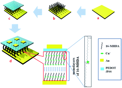
Herein, a kind of alkanethiol, 16-MHDA, was used to make the SAMs with several thicknesses which were dependent on the variation of the number of layers on the gold wafer (Scheme 1). To the best of our knowledge, this is the first reported time to construct a simple alkanethiol molecule for the nanodielectrics with a facile and convenient fabrication process. The current densities are obtained from the working M–M–M junction devices, and the tunneling transport through SAMs is explained by the Simmons tunneling model.
To study the electrochemical character of the molecule layer, a metal–molecule–metal (M–M–M) junction was widely used.32 During the process of making the sandwich junction structure, the top metal electrodes were commonly deposited on the top of the molecular layer with a direct vapor-deposited method such as e-beam lithography. Unfortunately, the filamentary pathways of the metal atoms would be formed through the molecular monolayer during deposition of the top electrodes of the SAMs, especially at the place of the pinhole defect sites in the SAMs,33 thereby causing electrical shorts. Research by Takhee Lee et al.21 showed that evaporation of the top Au electrodes on the SAM structure caused electric shorts or open circuits, along with a typical yield of only ∼1.2% of working devices (156 working devices out of 13440 devices fabricated). To avoid this kind of phenomenon, a conducting interlayer is needed to protect the SAMs from electric shorts.34 Here, we utilized poly(3,4-ethylenedioxythiophene) with poly(4-styrenesulfonic acid) (PEDOT:PSS), a widely used conducting polymer (30 S cm−1)35 as the protection layer between the metal electrodes and the SAMs in the M–M–M junctions. The terminal group of the 16-MHDA molecule is a hydrophilic carboxyl group. Therefore, the PEDOT:PSS layer was spin-coated on the SAMs and formed a dense and uniform layer that decreased the occurrence of pinholes with the hydrophilic–hydrophilic interaction effect.36
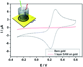
This nanodielectric was made through a self-assembled method, and the formation process was described in the (ESI†). As we know, to make a nanodielectric SAM, close covering the substrate by the SAMs was the key point, and then the assembled molecules were required to grow in an accordant direction. To first confirm the formation of the 16-MHDA SAM on the Au substrate, the most effective method is to characterize the electric property of the SAM-modified substrate. The CV was performed to measure the general formation state of the 16-MHDA SAM on the gold in the potassium hexacyanoferrate(III) (K3Fe(CN)6) and potassium chloride (KCl) solution (Fig. 1). Here, a bare gold wafer and a 16-MHDA SAM on gold wafer were set up as the working electrodes separately. A pair of perfect oxidation/reduction peaks of K3Fe(CN)6 were present in the cyclic voltammogram by using the bare gold as the working electrode. Different from the bare substrate, in the K3Fe(CN)6 redox region, the peaks disappeared after we made the SAM on the gold wafer as a working electrode, indicating that the gold surface was passivated with the non-electroactivity material when the SAM was successfully built up.
FT-IR spectrum was not only used to prove the presence of the molecules on the surface, but also used to evaluate the SAMs' structure. The C–H stretching mode spectrum in Fig. 2a showed the antisymmetric and symmetric C–H stretch modes at 2919 and 2850 cm−1, respectively.37 The C–H stretching region appeared at identical frequencies (2919, 2850 cm−1), and the absorbances increased linearly with the increasing layer number of SAMs (Fig. 2b and c). These phenomena suggested nearly ordered and identical alkyl chains were orientated and that no disordered layer-by-layer structure of 16-MHDA occurred even if the layer number reached 8. The interfacial bonding was examined by XPS, which illustrated that the Au–SH, S–Cu+, and S–S were formatted, respectively, at 161.9 ± 0.1, 162.4 ± 0.1, 163.5 eV separately (see ESI Fig. s1†).
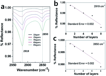 | ||
| Fig. 2 Comparison of FT-IR of different layers of the 16-MHDA SAMs. (a) was the FT-IR of the C–H stretching modes. (b) and (c) correspond to the absorbances. | ||
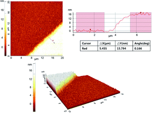
AFM was used to ascertain the thickness of 8 layers of the 16-MHDA on the gold substrate. The multilayer thickness was checked by the height difference profile between the local SAMs and the revealed gold surface. A cooled piranha solution was used to remove the local region of the preexisting SAMs. Since the length of the 16-MHDA molecule was about 2 nm, the theoretical height of 8 layers of 16-MHDA was about 16 nm. Fig. 3 showed the height difference between the top of the eight layers SAMs and the Au surface (SAMs removed region) was 15.8 ± 0.51 nm, which was consistent with the theoretical calculation.
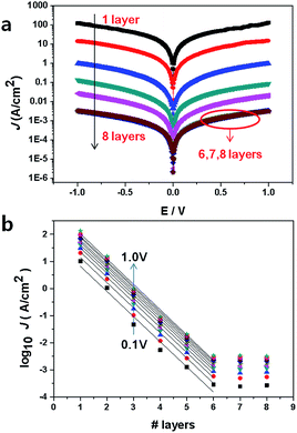
Fig. 4a shows the J–V characteristics of the 16-MHDA SAMs junctions on the gold substrate. The current was determined by the alkane length in the M–M–M junction, and the relationship between them was explained usually by the tunneling model.30 The tunneling effect could be used to explain the electron shuttle in the dielectric material with several-nanometer thickness between two electrodes. Here, an interesting phenomenon was observed in our work. Remarkably, the current density J was dramatically dependent on the number of the layers up to 6. By increasing the layers number, the current density decreased exponentially. Therefore, the results demonstrated that the nonresonant tunneling was the main mechanism for electron transport when the number of 16-MHDA layers was less than 6 (the thickness of SAMs was less than ∼12 nm). The tunneling effect can be further explained by using the Simmons equation.30
 | (1) |
 | (2) |
 | (3) |
Fig. 5 describes the relationship between capacitance and voltage, which was carried out on M–M–M type devices at high frequency (105 to 106 Hz). The C–f plots revealed maximum capacitances as follows. For 6 layers, Cmax-6 was 251 nF cm−2 at 105 Hz with slight all-off about 14% at the higher frequency of 106 Hz. For 7 layers, Cmax-7 was 222 nF cm−2 at 105 Hz with slight all-off about 11% at the higher frequency of 106 Hz, and for 8 layers, the Cmax-8 was 195 nF cm−2 at 105 Hz with slight all-off about 11% at the higher frequency of 106 Hz (Cmax-7 and Cmax-8 were shown in Fig. s2†).
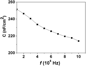 | ||
| Fig. 5 Frequency (f) dependence of the capacitance (C) at 1 V between 105 Hz and 106 Hz for 6-layers 16-MHDA. | ||
The capacitance decreased as the applied frequency increased. This phenomenon of the capacitance variation may be due to the formation of charges at the interface. These charges strongly affected the alternating current signal (ac signal) at lower frequency. So, the capacitance showed a decrease toward high frequencies.39
Conclusions
In summary, we have successfully constructed an organic nanodielectric of the 16-MHDA SAMs on a gold wafer, which could be potentially used in modern nanoelectronics. From the characterization of the CV, FT-IR, XPS, and AFM, the SAM layers were densely packed, and as demonstrated, the layer-by-layer structures of the 16-MHDA were well ordered when we increased the layer numbers from one to eight. The charge transfer characteristics of the self-assembled 16-MHDA mono- and multilayers were examined by using the M–M–M junction devices and explained with the Simmons tunneling model. The six layers 16-MHDA with about a 12 nm thickness was the critical barrier width for avoiding the tunneling effect, which was found in this work by testing the relationship between the current and the voltage in J–V characterization. Furthermore, a study of the C–f demonstrated great capacities for this type of SAMs. Our work will enhance the understanding of making nanodielectrics with long chained alkanethiol molecules by a self-assembled method and develop more applications in the nanometer electronic applications.Acknowledgements
This work was supported by the Energy & Resource Recycling of the Korea Institute of Energy Technology Evaluation and Planning (KETEP) grant funded by the Ministry of Trade, industry & Energy, Korea (no. 2010501010002B).Notes and references
- M. Osada, G. Takanashi, B.-W. Li, K. Akatsuka, Y. Ebina, K. Ono, H. Funakubo, K. Takada and T. Sasaki, Adv. Funct. Mater., 2011, 21, 3482–3487 CrossRef CAS PubMed.
- P. Lin and F. Yan, Adv. Mater., 2012, 24, 34–51 CrossRef CAS PubMed.
- F. Colleaux, J. M. Ball, P. H. Wobkenberg, P. J. Hotchkiss, S. R. Marder and T. D. Anthopoulos, Phys. Chem. Chem. Phys., 2011, 13, 14387–14393 RSC.
- A. I. Kingon, J.-P. Maria and S. K. Streiffer, Nature, 2000, 406, 1032 CrossRef CAS PubMed.
- Z. M. Dang, J. K. Yuan, S. H. Yao and R. J. Liao, Adv. Mater., 2013, 25, 6334–6365 CrossRef CAS PubMed.
- C. G. Hardy, M. S. Islam, D. Gonzalez-Delozier, H. J. Ploehn and C. Tang, Macromol. Rapid Commun., 2012, 33, 791–797 CrossRef CAS PubMed.
- C. Zou, D. Kushner and S. Zhang, Appl. Phys. Lett., 2011, 98, 082905 CrossRef PubMed.
- S. Ju, K. Lee, M.-H. Yoon, A. Facchetti, T. J. Marks and D. B. Janes, Nanotechnology, 2007, 18, 155201 CrossRef.
- K. Everaerts, L. Zeng, J. W. Hennek, D. I. Camacho, D. Jariwala, M. J. Bedzyk, M. C. Hersam and T. J. Marks, ACS Appl. Mater. Interfaces, 2013, 5, 11884–11893 CAS.
- T.-H. Huang, K.-C. Liu, Z. Pei, W.-K. Lin and S.-T. Chang, Org. Electron., 2011, 12, 1527–1532 CrossRef CAS PubMed.
- S. H. Kim, S. Nam, J. Jang, K. Hong, C. Yang, D. S. Chung, C. E. Park and W.-S. Choi, J. Appl. Phys., 2009, 105, 104509 CrossRef PubMed.
- G. A. Schwartz, C. Riedel, R. Arinero, P. Tordjeman, A. Alegria and J. Colmenero, Ultramicroscopy, 2011, 111, 1366–1369 CrossRef CAS PubMed.
- E. Tuncer, A. J. Rondinone, J. Woodward, I. Sauers, D. R. James and A. R. Ellis, Appl. Phys. A: Mater. Sci. Process., 2008, 94, 843–852 CrossRef.
- L.-L. Chua, P. K. H. Ho, H. Sirringhaus and R. H. Friend, Appl. Phys. Lett., 2004, 84, 3400 CrossRef CAS PubMed.
- F. Werkmeister and B. Nickel, J. Mater. Chem. B, 2013, 1, 3830 RSC.
- L.-H. Chen, P. Lin, M.-C. Chen, P.-Y. Huang, C. Kim, J.-C. Ho and C.-C. Lee, Org. Electron., 2012, 13, 1881–1886 CrossRef CAS PubMed.
- J.-M. Won, H. J. Suk, D. Wee, Y. H. Kim, J.-W. Ka, J. Kim, T. Ahn, M. H. Yi and K.-S. Jang, Org. Electron., 2013, 14, 1777–1786 CrossRef CAS PubMed.
- Y. Kim, J. Roh, J.-H. Kim, C.-m. Kang, I.-N. Kang, B. J. Jung, C. Lee and D.-H. Hwang, Org. Electron., 2013, 14, 2315–2323 CrossRef CAS PubMed.
- C. G. Hardy, M. S. Islam, D. Gonzalez-Delozier, J. E. Morgan, B. Cash, B. C. Benicewicz, H. J. Ploehn and C. Tang, Chem. Mater., 2013, 25, 799–807 CrossRef CAS.
- D. D. Agonafer, E. Chainani, M. E. Oruc, K. S. Lee and M. A. Shannon, J. Nanotechnol. Eng. Med., 2013, 3, 031006 CrossRef.
- T.-W. Kim, G. Wang, H. Lee and T. Lee, Nanotechnology, 2007, 18, 315204 CrossRef.
- H. B. Akkerman and B. de Boer, J. Phys.: Condens. Matter, 2008, 20, 013001 CrossRef.
- M. Akabori, V. A. Guzenko, T. Sato, T. Schäpers, T. Suzuki and S. Yamada, Phys. Rev. B: Condens. Matter Mater. Phys., 2008, 77, 205320 CrossRef.
- J. Collet, O. Tharaud, A. Chapoton and D. Vuillaume, Appl. Phys. Lett., 2000, 76, 1941 CrossRef CAS PubMed.
- A. Salomon, D. Cahen, S. Lindsay, J. Tomfohr, V. B. Engelkes and C. D. Frisbie, Adv. Mater., 2003, 15, 1881–1890 CrossRef CAS PubMed.
- E. Lee, I. Chung and Y. Son, Mol. Cryst. Liq. Cryst., 2010, 519, 199–205 CrossRef CAS.
- F. C. Simeone, H. J. Yoon, M. M. Thuo, J. R. Barber, B. Smith and G. M. Whitesides, J. Am. Chem. Soc., 2013, 135, 18131–18144 CrossRef CAS PubMed.
- H. J. Yoon, C. M. Bowers, M. Baghbanzadeh and G. M. Whitesides, J. Am. Chem. Soc., 2014, 136, 16–19 CrossRef CAS PubMed.
- N. Okabayashi, M. Paulsson and T. Komeda, Prog. Surf. Sci., 2013, 88, 1–38 CrossRef CAS PubMed.
- W. Wang, T. Lee and M. Reed, Phys. Rev. B: Condens. Matter Mater. Phys., 2003, 68 CAS.
- A. M. Nardes, M. Kemerink, R. A. J. Janssen, J. A. M. Bastiaansen, N. M. M. Kiggen, B. M. W. Langeveld, A. J. J. M. van Breemen and M. M. de Kok, Adv. Mater., 2007, 19, 1196–1200 CrossRef CAS PubMed.
- H. Haick, J. Ghabboun and D. Cahen, Appl. Phys. Lett., 2005, 86, 042113 CrossRef PubMed.
- G. Wang, H. Yoo, S.-I. Na, T.-W. Kim, B. Cho, D.-Y. Kim and T. Lee, Thin Solid Films, 2009, 518, 824–828 CrossRef CAS PubMed.
- H. B. Akkerman, P. W. Blom, D. M. de Leeuw and B. de Boer, Nature, 2006, 441, 69–72 CrossRef CAS PubMed.
- D. J. Yun and S. W. Rhee, ACS Appl. Mater. Interfaces, 2012, 4, 982–989 CAS.
- J. Jiang, W. Lu and Y. Luo, Chem. Phys. Lett., 2004, 400, 336–340 CrossRef CAS PubMed.
- T. A. Daniel, S. Uppili, G. McCarty and D. L. Allara, Langmuir, 2006, 23, 638–648 CrossRef PubMed.
- V. B. Engelkes, J. M. Beebe and C. D. Frisbie, J. Am. Chem. Soc., 2004, 126, 14287–14296 CrossRef CAS PubMed.
- A. Tataroğlu, İ. Yücedağ and Ş. Altindal, Microelectron. Eng., 2008, 85, 1518–1523 CrossRef PubMed.
Footnote |
| † Electronic supplementary information (ESI) available. See DOI: 10.1039/c4ra07868c |
| This journal is © The Royal Society of Chemistry 2014 |

