DOI:
10.1039/C4RA07609E
(Paper)
RSC Adv., 2014,
4, 51632-51639
Microwave assisted synthesis, characterization and thermoelectric properties of nanocrystalline copper antimony selenide thin films†
Received
25th July 2014
, Accepted 30th September 2014
First published on 2nd October 2014
Abstract
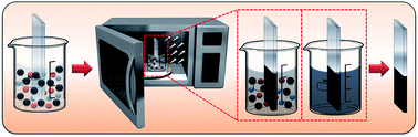
In the present work, we have synthesized p-type copper antimony selenide (Cu3SbSe4) thin films in an aqueous alkaline medium using a microwave assisted synthesis technique. The deposited thin films were characterized by UV-Vis-NIR spectroscopy, X-ray diffraction (XRD), field-emission scanning electron microscopy (FESEM), energy dispersive X-ray spectroscopy (EDS), high-resolution transmission electron microscopy (HRTEM) and thermoelectric techniques. On the basis of experimental results, a possible reaction mechanism has been discussed in detail. The band gap of the as deposited film is 1.94 eV and after annealing it reaches 1.87 eV for Cu3SbSe4. XRD results indicate that the as deposited thin films of CuSbSe2 have an orthorhombic crystal structure with secondary mixed phases and after annealing this is converted to Cu3SbSe4 having a pure tetragonal crystal structure. FESEM micrographs of Cu3SbSe4 showed a spherically diffused granular morphology having an average grain size of 25 nm. The HRTEM result of Cu3SbSe4 shows good crystallinity with a lattice spacing of 0.327 nm along the (112) plane. The EDS spectrum shows the presence of Cu, Sb and Se elements. The thermoelectric figure of merit (ZT) of the as deposited film is calculated to be 0.059 at 300 K and that of annealed Cu3SbSe4 is found to be 0.141 at 300 K.
1. Introduction
Inorganic nanocomposite materials are attracting considerable attention of researchers all over the world for the development of low cost power generation technologies. Synthesis of ternary metal chalcogenides by a simple synthetic approach is an increasing interest of researchers due to their unique physical and chemical properties.1 In recent years scientists have made more effort to utilize waste environmental energy by introducing alternative energy conversion sources like solar cells,2 fuel cells,3 water splitting for hydrogen production,4 nanogenerators,5 as well as thermoelectricity.6 In the past few years copper containing chalcogenides gained increasing attention due to their potential applications in thermoelectric, photovoltaic and photocatalytic devices.7 Nowadays semiconducting materials of I–V–VI group chalcogenides have driven extensive research interest because of their better electronic transport properties, low thermal conductivity, near-optimum band gap energy and large absorption coefficient (>104 cm−1). Copper antimony selenide (Cu–Sb–Se) is also one of the members of this group. With respect to its availability and low cost it was suggested as an alternative to CIGS.8 Cu–Sb–Se can be used as a promising material for photovoltaic as well as thermoelectric power generation purposes.9–12 The thermoelectric materials of this type can be used to convert heat energy to electrical energy and their efficiency depends on the dimensionless figure of merit (ZT).
Till today only few thin film synthesis methods based on physical and chemical techniques such as direct fusion method, low temperature solvothermal method, sequential evaporation followed by annealing and electrodeposition have been utilized to synthesize copper antimony selenide.12–21 However despite previously reported methods, it is necessary to develop a simple and cost effective synthesis route for deposition of Cu3SbSe4 thin films. Hence we have used new low cost and effective method for the deposition of Cu3SbSe4 thin films i.e. microwave assisted synthesis technique. Microwave technique is an emerging and versatile technique which gained lots of attention in recent years as compared with other techniques, because it is simple, less time consuming, energy efficient and reduces equipment costs.22,23 Recently synthesis of nanostructures of oxides,24,25 sulphides26 and selenides27 were successfully achieved by using microwave technique for different optoelectronic applications. It is well known fact that, microwave radiations absorbed by polar molecules present in reaction bath and undergoes excitations which leads to increase in thermal energy of the bath solution. Thermal energy consequently accelerates the reaction rate in an aqueous medium. Such type of heating process reduces the reaction time compared to conventional chemical process.
In the present investigation attempts have been made for first time to synthesize mixed metal chalcogenide (MMC) thin films of copper antimony selenide using relatively simple, low cost and rapid microwave technique. In this article we describe kinetics and reaction mechanism during the growth of ternary thin films. It has been observed that nanocrystalline Cu3SbSe4 thin film having average thickness of 400 nm grown on substrate support with optical energy gap value of 1.87 eV. The structural, compositional, morphological and thermoelectric properties as a function of temperature for as deposited CuSbSe2 and annealed Cu3SbSe4 thin films are discussed in this paper. To the best of our knowledge, there is no single report on the microwave assisted synthesis of Cu3SbSe4 thin films.
2. Experimental
2.1 Materials
All the chemicals are AR grade, used as received without further purification and prepared in double distilled water. In a typical experiment copper sulphate pentahydrate (CuSO4·5H2O, 99.5% Ranbaxy), antimony trichloride (SbCl3, 99.0% Merck) used as a source of Cu and Sb respectively. Tartaric acid (C4H6O6, 99.0% S D Fine Chem.) was used as a complexing agent. Aqueous sodium selenosulphite (Na2SeSO3) solution was used as source of Se which were obtained by refluxing Se metal powder (99.5% Sigma Aldrich) with saturated solution of Na2SO3 (97.0% S D Fine Chem.) as per our earlier report.28 Ammonia (NH3, 28.0–30.0% Thomas Baker) was used to adjust the pH of the reaction bath in the prescribed range and ammonium acetate (C2H4O2·NH3, 96.0% S D fine Chem.) used as buffer solution.
2.2 Deposition
The synthesis of copper antimony selenide thin films was carried out in domestic Microwave oven [ONIDA Microwave oven power convection 25] under ambient conditions. For the deposition of thin films reaction bath was prepared in 50 ml reaction container to which appropriate volumes of 0.25 M copper sulphate, 0.25 M antimony trichloride, 1 M tartaric acid as complexing agent and ammonium acetate were taken. Then pH of the solution was adjusted to 9.0 by adding NH3 followed by addition of appropriate volume of 0.25 M Na2SeSO3 solution and finally double distilled water was added to make total volume 40 ml. Immediately, the solution was stirred for 2 min and ultrasonically cleaned glass substrates were kept vertically in the reaction bath and reaction was kept in a microwave oven. The reaction bath was irradiated with microwave radiations with power of 180 W to provide heating. After 1 min time interval microwave oven was switch off for 2 min to prevent overheating of the reaction bath which leads to formation of multinucleation centers of MMC cluster according to Ostwald's ripening law. In the present experiment we have maintained microwave power 180 W for 1 h to deposit thin films. The influence of preparative parameters such as pH, molar ratio of precursors and irradiation time of microwave were optimized in order to deposit good quality thin films. At the end of the reaction, a uniform bluish black coloured thin films deposited on glass substrate were taken out and rinsed with double distilled water, dried at 50 °C in a constant temperature oven for 1 h. The as deposited films contain other mixed phases and to obtain pure Cu3SbSe4 thin films the as deposited films were annealed at 450 K for 1 h. The detailed schematic representation for the deposition of Cu3SbSe4 thin film formation using microwave assisted synthesis technique is represented in Fig. 1. To examine the reproducibility of deposited thin films, we have repeated the process for several times, also pure Cu3SbSe4 thin films were obtained after annealing.
 |
| Fig. 1 Schematic representation for the deposition of Cu3SbSe4 thin films using Microwave technique. | |
2.3 Characterizations
The thickness of the film was measured by surface profiler (AMBIOS XP-1). Optical absorption studies of as deposited and annealed thin films were carried out using UV-Vis-NIR spectrophotometer in wavelength range 400 nm to 1100 nm (Shimadzu UV-1800). To study the structural properties of films, X-ray diffraction (XRD) pattern were recorded by a Bruker AXS, D8 Model using Cu Kα (λ = 1.5406 Å) radiation. The surface morphology and compositional study were carried out by field-emission scanning electron microscopy (FESEM) (FESEM-S- 4700, Hitachi) attached with energy dispersive X-ray spectroscopy (EDS). The crystal lattice plane of deposited material were investigated by high-resolution transmission electron microscopy (HRTEM) using a TECNAI F20 Philips microscope operated at 200 kV. The DC electrical conductivity and thermal electromotive force (thermo emf) as a function of temperature was studied using two-probe method in temperature range 300 K to 400 K. To insure good ohmic contacts between the sample and probe silver paste finger was applied to film and to measure the working temperature Chromel–Alumel thermocouple was used. The thermo emf of the film with temperature was measured by applying temperature gradient across the film and corresponding thermal voltage was recorded. The room temperature thermal conductivity of the film was measured by ring probe method using commercial conductivity equipment (C-T meter, Teleph, France).
3. Results and discussion
The as deposited and annealed thin films were characterized by UV-Vis-NIR spectrophotometer, XRD, FESEM, EDS, HRTEM, DC electrical conductivity and thermo emf. For FESEM Pt coated sample is used. TEM sample was prepared by drop casting ethanolic dispersion of film onto a carbon-coated Cu grid. DC electrical conductivity measurements were carried out by keeping measurement system in light tight box which was kept at room temperature in air atmosphere.
Microwave synthesis process depends on the interaction of electromagnetic waves with molecules. In microwave synthesis process dipole moment is very important. A dipole moment is very sensitive to electromagnetic waves and it tries to align with waves. This process creates momentum in the molecules and leads to internal homogeneous heating of reaction bath. Water molecule has dipole moment which helps in the microwave heating. In microwave radiations, aqueous solvent heated frequently and also radiations provide uniform internal heating by direct transformation of microwave energy to molecules. Therefore, it reduces the thermal gradient in the reaction bath and provides consistent heating which leads to formation of multi nucleation centers, at this stage rate of reaction dramatically increased and hence microwave heating save reaction time and increases product yield.
|
Cu(Tartarate)aq → Cu2+ + (Tartarate)aq
| (1) |
|
Sb(Tartarate)aq → Sb3+ + (Tartarate)aq
| (2) |
Na2SeSO3 + H+ → HSe− + Na2SO3 |
|
HSe− + OH− → Se2− + H2O
| (3) |
Na2SO3 + 2OH− → Na2SO4 + H2O + 2e− |
|
Cu+ + Sb3+ + 2Se2− → CuSbSe2
| (5) |
In the reaction bath copper sulphate and antimony trichloride form complex with tartaric acid as Cu(Tartarate) and Sb(Tartarate) respectively. The Na2SeSO3 added in the reaction bath plays dual role in deposition, as it releases Se2− ions and reducing agent Na2SO3. At alkaline pH and under microwave irradiation Cu(Tartarate) and Sb(Tartarate) complexes undergo slow dissociation resulting into release of Cu2+ and Sb3+ ions respectively in the reaction bath as shown in reactions (1) and (2). Simultaneously Na2SeSO3 hydrolyses to release Se2− ions as in reaction (3). The released reducing agent Na2SO3 hydrolyses to form an electron, which is responsible for reduction of Cu2+ to Cu+ as shown in reaction (4) which is confirmed from color change of reaction bath from blue to colorless.29 The deposition of chalcogenide takes place by ion-by-ion condensation followed by Ostwald's ripening of corresponding ions onto the substrate surface. Generally in Ostwald's ripening process ‘growth of larger particles is done at the expense of smaller particles which have higher solubility’.
Throughout the process it was found that the reaction mixture remains colorless for first 10 min of microwave irradiation which indicates the induction period for the formation of nucleation centers. After 10 min under microwave irradiation when the ionic product (Kp) of released Cu+, Sb3+ and Se2− ions exceeds the solubility product (Ksp). The nucleation processes were start on the substrate surface by ion-by-ion condensation mechanism and reaction mixture turns turbid to form CuSbSe2 thin film as in reaction (5). At this stage mixed phases of Sb2Se3, Cu3Se2 and CuSe are also formed due to incomplete reduction of copper and presence of antimony. These nucleation centers form a monolayer onto surface of glass substrate and acts as a catalyst for the fast condensation of film.28 Under microwave radiations remaining metal complexes dissociates due to increase in heat energy and forms ions in the reaction bath. These released ions continue to grow on the monolayer formed on substrate support by following Ostwald's ripening law. In which monolayer grows at the expense of released ions under microwave irradiation. The kinetics of film growth is studied by measuring film thickness at different time intervals. Fig. 2 show the film grows continuously with deposition time and at the end thickness is nearly invariable. After 1 h film growth is stopped due to complete ionization of metal complexes. If the microwave power is increased above 180 W then the fast released ions undergoes precipitation and film were not formed. The as deposited films are of CuSbSe2 with presence of other mixed phases, which are converted to pure Cu3SbSe4 after annealing.
 |
| Fig. 2 Plot of as deposited film thickness vs. deposition time. | |
The optical absorbance of as deposited and annealed Cu3SbSe4 thin films were measured in the wavelength range 400 nm to 1100 nm at room temperature which is shown in inset of Fig. 3. The nature of optical transition in film is confirmed using eqn (1)
where, ‘
α’ is absorption coefficient, ‘
h’ is Plank's constant, ‘
ν’ is frequency, ‘
A’ is parameter that depends on the transition, ‘
Eg’ is optical energy gap and exponent ‘
n’ depends on the type of transition. For direct allowed transition exponent
n = 1/2, direct forbidden
n = 3/2, indirect allowed
n = 2 and for indirect forbidden
n = 3. The plot of (
αhν)
2 with photon energy (
hν) for both deposited thin films is shown in
Fig. 3 and value of
Eg was calculated by taking the intercept on the
X-axis. The nature of plot suggests the direct allowed transition in both as deposited and annealed thin film. The band gap energy of as deposited thin film is 1.94 eV and for pure Cu
3SbSe
4 it is 1.87 eV which is slightly higher than reported bulk values.
19 The higher band gap value may be due to the quantum confinement effect.
30,31
 |
| Fig. 3 Plot of (αhν)2 vs. photon energy (hν) of as deposited (a) and annealed (b) thin films (inset show plot of absorbance vs. wavelength of particular films). | |
Fig. 4 show X-ray diffraction patterns of as deposited and annealed thin film in range 20° to 80° 2θ. The diffraction peaks imply better crystallinity of the films. The as deposited CuSbSe2 film having orthorhombic crystal structure matches with JCPDS card 75-0992 with presence of other mixed phases. The annealed Cu3SbSe4 film having pure tetragonal crystal structure matches with JCPDS card 85-0003. The calculated lattice parameters for as deposited film are a = 6.41 Å, b = 3.97 Å and c = 15.32 Å, and for annealed Cu3SbSe4 film were found to be a = 5.66 Å and c = 11.28 Å is in good agreement with the JCPDS values.
 |
| Fig. 4 XRD Pattern of as deposited CuSbSe2 and annealed Cu3SbSe4 thin films synthesized by microwave technique indexed with standard JCPDS cards. | |
XRD pattern of pure Cu3SbSe4 thin film show prominent diffraction peaks at diffraction angle 27.2, 45.1, 45.3, 53.6 and 53.7 degree can be indexed as (112), (220), (204), (312) and (116) planes respectively. The comparison of 2θ and d values of standard JCPDS data with observed XRD data is given in Table 1 with difference in d value (Δd). The crystallite size of as deposited and annealed film was calculated by Scherrer's formula using eqn (2)
|
 | (2) |
where, ‘
D’ is diameter of the crystallite, ‘
K’ is dimensionless constant (0.94), ‘
λ’ is wavelength of the X-ray (1.5406 Å), ‘
β’ is full width at half maximum (FWHM) and ‘
θ’ is the diffraction angle.
32 The calculated crystallite size for the prominent diffraction peak of as deposited CuSbSe
2 was found to be 17.5 nm for (013) plane and that of annealed Cu
3SbSe
4 it is 30.6 nm for (112) plane. In order to evaluate the reproducibility of our experimental results, we have carried out similar experiments for several times at same conditions. Fig. S1 and S2
† show the XRD patterns of as deposited and annealed films at different time interval respectively. Fig. S3
† shows photographs of as deposited and annealed Cu
3SbSe
4 thin film samples of respective samples. These XRD patterns show no any variation with original samples confirming the reproducibility of our experimental conditions. From above discussion it is clear that developed microwave deposition technique is reproducible (ESI Fig. S1–S3
†).
Table 1 The angle of diffraction (2θ) and ‘d’ values along with its (hkl) planes of Cu3SbSe4 thin films is compared with standard JCPDS d-values, and difference in ‘d’ values (Δd)
No. |
Standard |
Observed |
Plane |
Δd (Å) |
2θ |
d (Å) |
2θ |
d (Å) |
h |
k |
l |
1. |
27.2 |
3.264 |
27.2 |
3.275 |
1 |
1 |
2 |
0.011 |
2. |
45.2 |
2.001 |
45.1 |
2.008 |
2 |
2 |
0 |
0.007 |
3. |
45.3 |
1.997 |
45.3 |
2.000 |
2 |
0 |
4 |
0.003 |
4. |
53.6 |
1.706 |
53.6 |
1.708 |
3 |
1 |
2 |
0.002 |
5. |
53.8 |
1.701 |
53.7 |
1.702 |
1 |
1 |
6 |
0.001 |
A typical FESEM image of as deposited and annealed thin films at different magnifications is shown in the Fig. 5. For both films spherically diffused grains were observed with quite uniform size distribution having average grain size to be 25 nm. The observed grain size of thin film deposited by microwave assisted technique was much smaller than the samples prepared by the traditional techniques reported so far. As seen in the FESEM, the synthesized material were little bit aggregated and which may be due to the absence of capping agent. The spherical grains are diffused to each other which exhibit very small interparticle distance and which would be very good for the charge transfer.
 |
| Fig. 5 FESEM images of as deposited (a and b) and annealed (c and d) thin films at different magnifications. | |
Further verification regarding composition of thin films was carried out using EDS technique. Fig. 6 shows the EDS spectra of the as deposited and annealed thin film with observed atomic percentage in inset table. Both patterns show three prominent peaks at 0.93 eV, 3.60 eV and 1.37 eV confirms the presence of Cu, Sb and Se elements respectively. This quantitative analysis shows that the films were slightly copper rich. No doubt the accurate composition control of ternary or any other multinary compounds remains challenging task. The deviations of product stoichiometry from starting ratios were widely observed for the ternary as well as quaternary chalcogenides.33 The non-stoichiometry may be attributed due to the difference in reactivity of the metal ions with chalcogen ions. In this case, the reactivity of copper ions was high as compared to antimony with respect to selenium ions and hence it may be responsible for the observed deviation in stoichiometry and formation of copper rich thin films.
 |
| Fig. 6 EDS spectra of both as deposited (a) and annealed (b) thin films prepared by microwave technique with obtained composition. | |
To study additional information about the morphology and structural properties, both the sample were further characterized by HRTEM technique. The representative HRTEM images of the as deposited and annealed thin films are shown in Fig. 7. The HRTEM images are in well agreement with FESEM results and show average grain size about 25 nm. The Fig. 7(a) and (b) show spherically diffused granular morphology of the material. The lattice fringes observed in the HRTEM Fig. 7 (c–f) point out that the material is crystalline in nature. The inter planer spacing of annealed Cu3SbSe4 film was calculated to be 0.327 nm corresponds for (112) lattice plane of tetragonal crystal structure. The HRTEM results are consistent with the XRD pattern and confirm the crystallinity and phase of both the films.
 |
| Fig. 7 HRTEM images of as deposited (a–d) and annealed Cu3SbSe4 (e and f) thin films at different magnifications, show spherically diffused granular morphology. | |
The Seebeck coefficient, electrical conductivity and resulting power factor of as deposited and annealed thin films in temperature range 300 K to 400 K is displayed in Fig. 8. As shown in Fig. 8(a) the electrical conductivity ‘σ’ of both films increases exponentially with increase in temperature, confirms semiconducting nature of the material. The room temperature ‘σ’ of as deposited CuSbSe2 thin film was measured to be 313.6 S cm−1 which is increased to 345.0 S cm−1 for pure Cu3SbSe4 at 300 K. This moderate conductivity is attributed due to the diffused granules which facilitates the smooth charge transfer.
 |
| Fig. 8 Temperature dependant electrical conductivity ‘σ’ (a), Seebeck coefficient ‘S’ (b) and power factor ‘S2σ’ (c) of as deposited CuSbSe2 and annealed Cu3SbSe4 thin films. | |
The temperature dependence of the Seebeck coefficient ‘S’ of thin films were measured by integral method which shown in Fig. 8(b). Thermal gradient between two ends of sample causes transport of charge carriers from hot end to cold end and this bring out generation of electrical field which gives rise to thermal voltage. Seebeck coefficient of as deposited and annealed thin films was calculated by using eqn (3).34
|
 | (3) |
where, ‘Δ
V’ is measured thermal voltage and ‘Δ
T’ is temperature difference across the film. The positive value of Seebeck coefficient for both as deposited and annealed thin films determined in the temperature range 300 K to 400 K reveals that the major charge carriers in film are holes and it consistent with p-type semiconducting nature. Till date the p-type nature is most common in nearly all of the Cu–Sb–Se based reported compounds.
21 Temperature dependence of Seebeck coefficient show approximately linear behavior throughout the temperature range. The Seebeck coefficient of as deposited CuSbSe
2 thin film was found to be 34.0 μV K
−1 and for annealed Cu
3SbSe
4 it is 47.6 μV K
−1 at 300 K.
The power factor (S2σ) is one of the important parameter, because it evaluates the performance of the thermoelectric materials, especially for thin films, as kind of figure of merit. It can be easily obtained from the electrical conductivity and Seebeck coefficient.35 The temperature dependence of power factor were shown in Fig. 8(c), it also shows the linear relationship throughout temperature range. For instance it was calculated to be 0.36 μW cm−1 K−2 for as deposited film and for annealed Cu3SbSe4 film it is 0.78 μW cm−1 K−2 at 300 K. This improvement in power factor is mainly due to the annealing process which leads to the pure phase of the material. The maximum power factor for pure Cu3SbSe4 film is obtained to be 19.92 μW cm−1 K−2 at 400 K. This value is comparable with nearly all reported value, in Ge doped Cu3SbSe4 (around 16 μW cm−1 K−2 at 600 K),13 in Cu3SbSe4 (between the range 2 μW cm−1 K−2 to 5 μW cm−1 K−2)11 and in Cu3Sb0.94Sn0.06Se3.5S0.5 (17 μW cm−1 K−2 at 620 K).36
The thermal conductivity ‘κ’ is also one of the important properties of the material to improve the performance of thermoelectric device. Thermal conductivity of material is due to the heat transport from one side to another by both phonons and carriers. The thermal conductivity is inversely proportional to ZT, due to this fact lower κ value is suitable. The κ of as deposited thin film is observed to be 0.184 W m−1 K−1 and for annealed thin film it reaches to 0.166 W m−1 K−1. This lower κ value is due to the small size of the material with presence of higher grain boundaries. The thermoelectric performance of both thin films were quantified by using a dimensionless ZT as in eqn (4)
|
 | (4) |
An ideal thermoelectric material should have high electrical conductivity, high power factor and low thermal conductivity. The ZT of as deposited film is calculated to be 0.059 at 300 K and for annealed film it reaches to 0.141 at 300 K. The room temperature ZT and other parameters (σ, S, PF and κ) of as deposited and annealed films are given in Table 2. This obtained ZT value is compatible with reported value in Ti doped CuSbSe2 (which is 0.0041)17 but lower than reported in Cu3Sb0.07Ge0.03Se3.8S1.2 (0.89 at 650 K),14 in Cu3Sb0.975Sn0.025Se4 (0.75 at 673 K),18 in 2% Sn doped Cu3SbSe4 (0.72 at 630 K),13 in pure Cu3SbSe4 (0.17 for 575 K) and in Bi doped Cu3SbSe4 (0.7 for 600 K).11 All these reported materials were synthesized by direct fusion method and it requires high temperature and annealing treatment. At this stage the ZT value of Cu3SbSe4 is lower at room temperature and it might be improved at higher temperature or may be with addition of controlled amounts of dopants. Up to now the highest reported ZT value obtained for Cu3SbSe4 based nanostructured bulk material is 1.1 at 700 K (ref. 36) which were synthesized by low temperature co-precipitation route.
Table 2 Room temperature (300 K) electrical conductivity (σ), Seebeck coefficient (S), power factor (S2σ), thermal conductivity (κ) and ZT of as deposited and annealed thin films
Sample |
σ (S cm−1) |
S (μV K−1) |
S2σ (μW cm−1 K−2) |
κ (W m−1 K−1) |
ZT (300 K) |
CuSbSe2 |
313.6 |
34.0 |
0.36 |
0.184 |
0.059 |
Cu3SbSe4 |
345.0 |
47.6 |
0.78 |
0.166 |
0.141 |
4. Conclusions
Nanocrystalline ternary chalcogenide (Cu3SbSe4) thin films were successfully prepared for the first time by microwave assisted synthesis route. The microwave assisted growth mechanism was discussed on the basis of Ostwald's ripening law. The thin films deposited by this technique showed good crystallinity and morphology with remarkable electrical and thermal conductivity. The compositional analysis showed copper rich thin films might be due to better reactivity of copper with selenium which also reflects on high optical absorption coefficient with optical band gap of material. Consequently the formation of spherically diffused granular morphology was shown to be very effective to obtain better thermoelectric properties. Based on this approach, the σ, S, PF and κ were calculated to be 345.0 S cm−1, 47.6 μV K−1, 0.78 μW cm−1 K−2 and 0.166 W m−1 K−1 respectively at 300 K. The calculated ZT was found to be 0.141 at 300 K. The structural, morphological, compositional and thermoelectric results at 300 K shows that the Cu3SbSe4 thin film material is a good candidate for thermoelectric power generation.
Acknowledgements
One of the authors VBG thanks to University Grants Commission (UGC), New Delhi for awarding ‘UGC Research Fellowship in Science for Meritorious Student’ and providing financial assistance for this work. This research was also supported by the basic Science Research program through the National Research Foundation of Korea (NRF) funded by the Ministry of Education (NRF-2009-0094055).
Notes and references
- D. Aldakov, A. Lefrançois and P. Reiss, J. Mater. Chem. C, 2013, 1, 3756 RSC.
- J. K. Olesiak and H. Weller, ACS Appl. Mater. Interfaces, 2013, 5, 12221 Search PubMed.
- C. Y. Wang, Chem. Rev., 2004, 104, 4727 CrossRef CAS.
- J. Xing, H. B. Jiang, J. F. Chen, Y. H. Li, L. Wu, S. Yang, L. R. Zheng, H. F. Wang, P. Hu, H. J. Zhao and H. G. Yang, J. Mater. Chem. A, 2013, 1, 15258 CAS.
- X. Wang, J. Song, J. Liu and Z. L. Wang, Science, 2007, 316, 102 CrossRef CAS PubMed.
- F. J. Fan, B. Yu, Y. X. Wang, Y. L. Zhu, X. J. Liu, S. H. Yu and Z. Ren, J. Am. Chem. Soc., 2011, 133, 15910 CrossRef CAS PubMed.
- X. Lin, A. Steigert, M. C. L. Steiner and A. Ennaoui, RSC Adv., 2012, 2, 9798 RSC.
- D. Colombara, L. M. Peter, K. D. Rogers, J. D. Painter and S. Roncallo, Thin Solid Films, 2011, 519, 7438 CrossRef CAS PubMed.
- D. J. Temple, A. B. Kehoe, J. P. Allen, G. W. Watson and D. O. Scanlon, J. Phys. Chem. C, 2012, 116, 7334 CAS.
- D. Tang, J. Yang, F. Liu, Y. Lai, J. Li and Y. Liu, Electrochim. Acta, 2012, 76, 480 CrossRef CAS PubMed.
- X. Y. Li, D. Li, H. X. Xin, J. Zhang, C. J. Song and X. Y. Qin, J. Alloys Compd., 2013, 561, 105 CrossRef CAS PubMed.
- P. Maiello, G. Zoppi, R. W. Miles, N. Pearsall and I. Forbes, Sol. Energy Mater. Sol. Cells, 2013, 113, 186 CrossRef CAS PubMed.
- E. J. Skoug, J. D. Cain, P. Majsztrik, M. Kirkham, E. L. Curzio and D. T. Morelli, Sci. Adv. Mater., 2011, 3, 602 CrossRef CAS PubMed.
- E. J. Skoug, J. D. Cain and D. T. Morelli, Appl. Phys. Lett., 2011, 98, 261911 CrossRef PubMed.
- E. J Skoug, J. D. Cain, D. T. Morelli, M. Krkham, P. Majsztrik and E. L. Curzio, J. Appl. Phys., 2011, 110, 023501 CrossRef PubMed.
- L. I. Soliman, A. M. A. E. Soad, H. A. Zayed and S. A. E. Ghfar, Fiz. A, 2002, 4, 139 Search PubMed.
- D. Li and X. Y. Qin, J. Appl. Phys., 2006, 100, 023713 CrossRef PubMed.
- C. Yang, F. Huang, L. Wu and K. Xu, J. Phys. D: Appl. Phys., 2011, 44, 295404 CrossRef.
- J. Zhou, G. Q. Bian, Q. Y. Zhu, Y. Zhang, C. Y. Li and J. Dai, J. Solid State Chem., 2009, 182, 259 CrossRef CAS PubMed.
- A. M. Fernandez and J. A. Turner, Sol. Energy Mater. Sol. Cells, 2003, 79, 391 CrossRef CAS.
- D. Tang, J. Yang, F. Liu, Y. Lai, M. Jia, J. Li and Y. Liu, Electrochem. Solid-State Lett., 2012, 15, 11 CrossRef PubMed.
- H. Qian, X. Qiu, L. Li and J. Ren, J. Phys. Chem. B, 2006, 110, 9034 CrossRef CAS PubMed.
- C. C. Wu, C. Y. Shiau, D. W. Ayele, W. N. Su, M. Y. Cheng, C. Y. Chiu and B. J. Hwang, Chem. Mater., 2010, 22, 4185 CrossRef CAS.
- L. Zhang, X. F. Cao, Y. L. Ma, X. T. Chen and Z. L. Xue, CrystEngComm, 2010, 12, 3201 RSC.
- R. R. Kharade, K. R. Patil, P. S. Patil and P. N. Bhosale, Mater. Res. Bull., 2012, 47, 1787 CrossRef CAS PubMed.
- S. Ge, Z. Shuia, Z. Zheng and L. Zhang, Opt. Mater., 2011, 33, 1174 CrossRef CAS PubMed.
- Y. H. Seo, B. S. Lee, Y. Jo, H. G. Kim, Y. Choi, S. J. Ahn, K. H. Yoon, K. Woo, J. Moon, B. H. Ryu and S. Jeong, J. Phys. Chem. C, 2013, 117, 9529 CAS.
- S. D. Kharade, N. B. Pawar, V. B. Ghanwat, S. S. Mali, W. R. Bae, P. S. Patil, C. K. Hong, J. H. Kim and P. N. Bhosale, New J. Chem., 2013, 37, 2821 RSC.
- M. Dhanam, P. K. Manoj and R. R. Prabhu, J. Cryst. Growth, 2005, 280, 425 CrossRef CAS PubMed.
- S. B. Pawar, J. S. Shaikh, R. S. Devan, Y. R. Ma, D. Haranath, P. N. Bhosale and P. S. Patil, Appl. Surf. Sci., 2011, 258, 1869 CrossRef CAS PubMed.
- Y. R. Lazcano, M. T. S. Nair and P. K. Nair, J. Cryst. Growth, 2001, 223, 399 CrossRef.
- S. D. Kharade, N. B. Pawar, S. S. Mali, C. K. Hong, P. S. Patil, M. G. Gang, J. H. Kim and P. N. Bhosale, J. Mater. Sci., 2013, 48, 7300 CrossRef CAS.
- L. Ai and J. Jiang, J. Mater. Chem., 2012, 22, 20586 RSC.
- T. B. Shimony and J. S. Ishay, J. Theor. Biol., 1981, 92, 497 CrossRef.
- M. M. Salunkhe, R. R. Kharade, S. D. Kharade, S. S. Mali, P. S. Patil and P. N. Bhosale, Mater. Res. Bull., 2012, 47, 3860 CrossRef CAS PubMed.
- D. Li, R. Li, X. Y. Qin, J. Zhang, C. J. Song, L. Wang and H. X. Xin, CrystEngComm, 2013, 15, 7166 RSC.
Footnote |
† Electronic supplementary information (ESI) available: Reproducibility of experimental results: (Fig. S1–S3) as deposited and annealed XRD patterns, respective photographs. See DOI: 10.1039/c4ra07609e |
|
This journal is © The Royal Society of Chemistry 2014 |
Click here to see how this site uses Cookies. View our privacy policy here.