
Investigation of defect related photoluminescence property of multicolour emitting Gd2O3:Dy3+ phosphor
Thangaraj Selvalakshmia,
Selvakumar Sellaiyanb,
Akira Uedonob and
Arumugam Chandra Bose*a
aNanomaterials Laboratory, Department of Physics, National Institute of Technology, Tiruchirappalli-620015, India. E-mail: acbose@nitt.edu; Fax: +91 431 2500133; Tel: +91-431-2503605
bDivision of Applied Physics, University of Tsukuba, Ibaraki 305-8573, Japan
First published on 25th July 2014
Abstract
Multicolour emitting Gd2O3:Dy3+ phosphor is prepared by citrate based sol–gel method as a function of annealing temperature of the sample and its emission property dependence with lattice defects is elaborated. The annealed phosphors are characterized by X-ray powder diffraction (XRD), Raman spectroscopy, diffuse reflectance spectroscopy (DRS), photoluminescence (PL), fluorescence lifetime and positron annihilation lifetime spectroscopy (PALS). The phosphors annealed at different temperatures greatly influence the defect and emission intensities, as revealed from PL and PALS measurements, respectively. The efficient energy transfer (ET) from the Gd3+ ion to Dy3+ ion is schematically illustrated with the aid of an energy level diagram. The PL spectra clearly conclude that Dy3+ with an ionic radius close to the Gd3+ ion prefers to occupy the C2 site in the Gd2O3 matrix. The positron lifetime spectroscopy qualitatively explains the concentration of defects (vacancy and voids) which are minimized with the increase in the annealing temperature. The correlation between PL emission and lattice defects is also reported in detail.
Introduction
Luminescent materials have attracted a great deal of interest due to their wide applications in various fields such as LEDs, biological assays, display and photonic devices.1–5 Among them, much focus is given to the LED based on white light emission owing to its long photoluminescence lifetime, high brightness, low power consumption and environmental friendliness (i.e. mercury free) and it is considered as the next generation of solid state lightening devices.6–8 The efficiency of LEDs is also found to be higher than the conventionally used incandescent and fluorescent light sources.9Among the rare earth (RE) ions, Dy3+ provides strong blue, yellow and feeble red emission in the visible region of the electromagnetic spectrum due to the 4f–4f transition. Various colour emissions are possible due to the transition from the excited state of 4F9/2 to 6H15/2 (blue), 6H13/2 (yellow), 6H11/2 (red) state.10–13 Based on the occupancy of Dy3+ ion in the inversion or non-inversion site of Gd3+, the intensities of emission colours differ.14 By tuning and coupling the emission intensity of each colour, it is possible to obtain white colour emission. When compared to direct UV excitation of Dy3+, the energy transfer through host ion or sensitizer ion is more efficient.13 Recently an effective energy transfer has been reported from Gd3+ to Dy3+ in the Ca2Gd8Si6O26:Dy3+ and Gd(BO2)3:Dy3+ phosphor.15,16
In addition, the luminescence properties are strongly influenced by the presence of lattice defects17 like mono vacancy, vacancy cluster, voids or pores which are formed naturally during synthesis. The positron annihilation spectroscopy is a powerful and sensitive tool to identify the defects in the solids, distinguish the type of defects and provide relevant information about the size and density around the defects.18 The positively charged positrons are generated by an unstable isotope, typically 22Na, which is marked by the simultaneous release of a 1.28 MeV gamma rays. On entering into the condensed matter, the positron searches for a negatively charged electron and annihilates with the release of two 511 keV γ quanta. The positively charged positron is easily attracted towards the vacancy and open space in order to neutralize the charge. The lifetimes measured for the positrons trapped in a certain defect type are sensitive to the defect size. The value determines the type of defects19 and the corresponding intensity reveals the defect concentration. An inverse relation exists between the positron lifetime and the electron density of the trap site. The energy distribution of the annihilation γ rays is broadened by the momentum component of the annihilating electron–positron pair pL which is parallel to the emitting direction of the γ rays. The energy of the γ rays is given by Eγ = 511 ± ΔEγ keV. Here, the Doppler shift ΔEγ is given by ΔEγ = pLc/2, where c is the speed of light. A freely diffusing positron may be localized in a vacancy-type defect because of Coulombic repulsion from the positively charged ion cores. Because the momentum distribution of the electrons in such defects differs from that of electrons in the bulk material, these defects can be detected by measuring the Doppler broadening spectra of the annihilation radiation. From the above, the S parameter represents the fraction of low momentum electrons annihilated by the positrons and, hence, it varies in accordance with the changes in size and concentration of the defects in the solids.20
Lu et al. reported the positron lifetime of the Eu3+/Dy3+ codoped SrAl2Si2O8/SrAlSi1/2O7/2 composite phosphor.21 The lattice defect created by replacing Sr by Eu and Dy in the composite phosphor affects the photoluminescence emission intensity. Defect properties of La and Eu codoped CaAl2O4 phosphor is investigated by Lin et al.22 Here, the defects due to the charge imbalance between La3+ and Ca2+ is focused and the defect concentration increases with increasing the content of La. The formation of vacancy clusters within the nanoparticles is reported by Thorat et al. in Eu doped CeO2.23 On increasing the positive charge defect by doping Er3+ and Nd3+, the photoluminescence emission intensity of BaAlMg10O17:Eu2+ is enhanced.24 To the best of our knowledge, the positron annihilation studies on Gd2O3:Dy3+ phosphors are not explored elsewhere.
In the present work, Gd2O3:Dy3+ phosphors are synthesized by citrate-based sol–gel method and it is annealed at different temperatures. The photoluminescence properties of Dy3+ ion are investigated through energy transfer mechanism which is initiated from Gd3+ to Dy3+ and the process is well illustrated by the energy level diagram. The combined emission colour is also predicted and integrated from the CIE coordinate. Since the photoluminescence emission property strongly depends on the concentration of impurities and defects, we employed a high sensitive positron annihilation spectroscopy to identify and to investigate the defects in Gd2O3:Dy3+ phosphors. Finally, we also explore the correlation between the lattice defect and photoluminescence properties.
Experimental and characterization techniques
0.1 M of citric acid is dissolved in de-ionized water and used as a solvent. The required quantity of Gd(NO3)3 and Dy(NO3)3 are dissolved in citric acid with magnetic stirring to get homogeneous solution. The molar ratio of the metal ions to the citric acid is maintained as 1![[thin space (1/6-em)]](https://www.rsc.org/images/entities/char_2009.gif) :1. The pH of the solution is raised to 2 by the adding aqueous NH3 solution in drops. The solution is heated to 70 °C with contant stirring for the solvent evaporation. Initially, a transparent gel is formed and gradually transformed to xerogel. The residual organic precursor present in the sample is removed by heating at 250 °C for 2 h which yield a black-coloured fine particles. The Gd1.99O3:Dy3+0.01 phosphors are obtained by annealing at 600 °C, 700 °C and 800 °C in air atmosphere.
:1. The pH of the solution is raised to 2 by the adding aqueous NH3 solution in drops. The solution is heated to 70 °C with contant stirring for the solvent evaporation. Initially, a transparent gel is formed and gradually transformed to xerogel. The residual organic precursor present in the sample is removed by heating at 250 °C for 2 h which yield a black-coloured fine particles. The Gd1.99O3:Dy3+0.01 phosphors are obtained by annealing at 600 °C, 700 °C and 800 °C in air atmosphere.
The crystal structure and lattice parameters are estimated from Rigaku Ultima III powder X-ray diffractometer (XRD). The pattern is recorded at θ–2θ geometry with CuKα1 (1.5406 Å) generated at 40 kV and 30 mA over the range of 10° to 80° with a step size of 0.02°. Transmission electron microscopy (TEM) images are recorded using Tecnai G2 FEI with the accelerating voltage of 200 kV. For TEM measurements, the powder samples are dispersed well in ethanol and a drop casted on carbon-coated copper grid. Fourier transform infrared (FTIR) spectra are recorded between 4000 and 400 cm−1 using Jasco FTIR-4200. Raman spectra are recorded using Jobin Yvon Horiba (LABRAM HR - 800) Micro Raman spectrometer attached with Nd:YAG laser as the excitation source having an output power of 15 mW with a laser beam spot size 100 mm in the range of 700 cm−1 to 300 cm−1. The absorption property of the material is measured with diffuse reflectance spectroscopy (DRS) using UV 2600 Shimadzu instruments. The photoluminescence (PL) spectra are recorded with spectroflurometer (RF 5301 PC Shimadzu) equipped with 150 W Xe source. Quantum yield is determined using JASCO ISF – 834 60 mm integrating sphere at the incident angle of 5°. Fluorescence lifetime measurements are obtained under pulsed excitation at 266 nm by using Nd:YAG laser with a pulse width of 8 ns and pulse energy of 150 mJ. The positron annihilation lifetime spectroscopy (PALS) is measured using a conventional lifetime system with digital oscilloscope (LeCroy Wavepro). The positron annihilation signals are detected by two BaF2 scintillators attached to H3378 (Hamamatsu Photonics) photomultiplier tubes (PMT). The output of PMT is divided into two: one is connected to a constant fraction discrimintor (CFD) and the other to the digital oscilloscope. The samples are sandwiched with 22Na source (370 kBq) and lifetime measurements are carried out in room atmospheric pressure. Each spectrum has counts about 6 x10⁶ and the number of lifetime components is determined by deconvoluting the lifetime spectra. The observed spectra are analysed and interpreted with a time resolution of about 170 ps by using the RESOLUTION computer program.25 Coincidence Doppler broadening spectra are measured by using conventional spectrometer with Ge detector, with energy resolution of ∼1.2 keV at the photo peak of 511 keV. For each of the measurements, a total of 5 × 10⁶ counts in the annihilation peak are collected. The low-momentum part of the spectra is characterized by the S parameter, defined as the number of annihilation events over the energy range of 511 keV ± ΔEγ (where ΔEγ = 0.76 keV) around the centre of the peak, and the high-momentum part is characterized by using the W parameter, defined as the annihilation events in the range of 3.4 keV ≤ ∣ΔEγ∣ ≤ 6.8 keV.
Results and discussion
The phase purity of the phosphors is analysed by XRD pattern. Fig. 1 shows the XRD pattern of Gd2O3:Dy3+ annealed at different temperatures. All the diffraction peaks of the phosphors are indexed to cubic phase Gd2O3 (JCPDS card no. 86 2477) with the space group of Ia![[3 with combining macron]](https://www.rsc.org/images/entities/char_0033_0304.gif) (206) and lattice parameter of a = b = c = 10.8 Å. The most prominent peaks in the XRD pattern (Fig. 1) are indexed and the corresponding (hkl) planes are indicated. The absence of secondary X-ray diffraction peak related to the Dy2O3 phase confirms that the Dy3+ ions are well substituted in the Gd3+ site without influencing the crystal structure of Gd2O3. Moreover, dissolving 1% of Dy3+ in Gd2O3 lattice is highly possible due to their similar ionic radii (Gd3+ = 0.938 Å and Dy3+ = 0.912 Å). In Gd2O3:Dy3+ annealed at 600 °C, peaks in the 2θ range of 50° and 80° are not well observed but above 600 °C annealed samples, all the peaks are clearly distinguishable revealing the high crystalline nature of the phosphor.
(206) and lattice parameter of a = b = c = 10.8 Å. The most prominent peaks in the XRD pattern (Fig. 1) are indexed and the corresponding (hkl) planes are indicated. The absence of secondary X-ray diffraction peak related to the Dy2O3 phase confirms that the Dy3+ ions are well substituted in the Gd3+ site without influencing the crystal structure of Gd2O3. Moreover, dissolving 1% of Dy3+ in Gd2O3 lattice is highly possible due to their similar ionic radii (Gd3+ = 0.938 Å and Dy3+ = 0.912 Å). In Gd2O3:Dy3+ annealed at 600 °C, peaks in the 2θ range of 50° and 80° are not well observed but above 600 °C annealed samples, all the peaks are clearly distinguishable revealing the high crystalline nature of the phosphor.
 | ||
| Fig. 1 XRD pattern of Gd2O3:Dy3+ phosphors annealed at different temperatures. | ||
The peak broadening in the XRD pattern due to the crystallite size is calculated after eliminating the instrumental broadening. The contribution of the instrumental effect is eliminated using Cauchy's relation26 presented in eqn (1).
| βhkl = (βhkl)m − (βhkl)i | (1) |
|
2dhklsinθ = nλ
| (2) |
 | (3) |
| Annealing temperature | 2θ (°) | β (rad) ×10−3 | dhkl (Å) | D (nm) | a = b = c (Å) | Unit cell volume (Å3) |
|---|---|---|---|---|---|---|
| JCPDS-86 2477 | 28.585 | — | 3.120 | — | 10.8 | 1259.71 |
| 600 °C | 28.636 | 9.961 | 3.116 | 15 | 10.795 | 1257.96 |
| 700 °C | 28.561 | 4.71 | 3.124 | 33 | 10.823 | 1267.77 |
| 800 °C | 28.464 | 3.332 | 3.135 | 47 | 10.859 | 1280.47 |
Fig. 2(a) shows the TEM micrograph of Gd2O3:Dy3+ phosphor annealed at 600 °C. We observe that the phosphors exhibit more or less spherical shape morphology with non-uniform size distribution. The particle size distribution presented in Fig. 2(b) implies that the size of nanoparticles is in the range of 9–16 nm which is in consistent with the size (15 nm) estimated from XRD pattern. Fig. 2(c) shows the selected area diffraction (SAD) pattern of Gd2O3:Dy3+ phosphor, the presence of ring-like pattern confirms the polycrystalline nature and cubic structure of Gd2O3. The rings of SAD pattern are indexed to the corresponding plane.
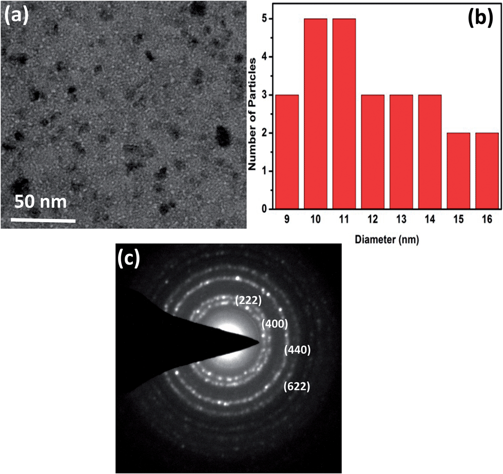 | ||
| Fig. 2 (a) TEM micrograph (b) size distribution graph (c) selected area diffraction pattern of Gd2O3:Dy3+ annealed at 600 °C. | ||
The presence of various chemical functional groups in the phosphor is studied from the FTIR spectra as shown in Fig. 3. The broad peaks centred at 3400 cm−1 corresponds to the O–H stretching of H2O molecule absorbed from the atmospheric air.28 However, this peak starts diminishing and completely disappeared on increasing the annealing temperature. The weak intense peak around 1600 cm−1 indicate the vibration of C![[double bond, length as m-dash]](https://www.rsc.org/images/entities/char_e001.gif) O group which originate from the absorption of atmospheric CO2.29 The absence of vibration peaks corresponding to the citric acid functional groups (in the range of 1730 cm−1–1700 cm−1 and 1710 cm−1–1680 cm−1) implies that the annealing effectively removes the solvent medium and render a phase pure Gd2O3.28 The sharp peak appearing at 545 cm−1 is attributed to the vibration of Gd–O bond30 and it becomes more intense and predominant with the increase in annealing temperature.
O group which originate from the absorption of atmospheric CO2.29 The absence of vibration peaks corresponding to the citric acid functional groups (in the range of 1730 cm−1–1700 cm−1 and 1710 cm−1–1680 cm−1) implies that the annealing effectively removes the solvent medium and render a phase pure Gd2O3.28 The sharp peak appearing at 545 cm−1 is attributed to the vibration of Gd–O bond30 and it becomes more intense and predominant with the increase in annealing temperature.
 | ||
| Fig. 3 FTIR spectra of Gd2O3:Dy3+ annealed at different temperatures. | ||
The phonon energy of the Gd2O3:Dy3+ phosphors annealed at 600 °C, 700 °C and 800 °C phosphor is characterized by Raman spectroscopy and presented in Fig. 4. The spectra consists of Raman mode of vibrations at 359 cm−1, 314 cm−1, 445 cm−1, 479 cm−1 and 568 cm−1.31–33 When the phosphors are annealed from 600 °C to 800 °C, crystallinity nature increases and so the sharpness of the Raman peak. In order to avoid, quenching of excited energy due to non-radiative transition, it is necessary to select host matrix with low phonon energy.34 The phonon energy corresponding to the maximum intensity peak (359 cm−1) is not sufficient enough to undergo transition in electronic energy level. It clearly indicates that Gd2O3 is a host matrix with low phonon energy and hence a promising host for luminescent applications.
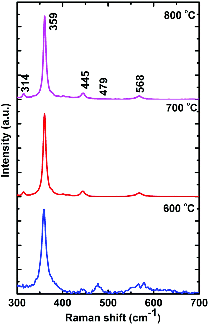 | ||
| Fig. 4 Raman spectra of Gd2O3:Dy3+ phosphor annealed at 600 °C, 700 °C and 800 °C. | ||
Fig. 5(a) shows the reflectance spectra of Gd2O3:Dy3+ phosphors annealed at different temperatures and the wavelength is recorded between 200 nm and 800 nm. It shows strong host ion absorption between 200 nm and 250 nm with the sharp adsorption edge at 231 nm. The weak adsorption at 274 nm corresponds to the 8S7/2–6IJ transition of Gd3+ ions.35 The band gap of Gd2O3:Dy3+ phosphors is calculated by Kubelka–Munk (K–M) plot and presented in Fig. 5(b). According to the K–M function, the relationship between optical absorption coefficient and band gap energy is given in eqn (4).
| (F(R)hν)2 = A(hν − Eg) | (4) |
 | ||
| Fig. 5 (a) Reflectance spectra and (b) band gap plot of Gd2O3:Dy3+ phosphors annealed at different temperatures. | ||
The PALS measurement is used to evaluate the defect related properties of Gd2O3:Dy3+ phosphors annealed at different temperatures. The positron lifetime curve is resolved into three components τ1, τ2 and τ3 and the corresponding intensities I1, I2 and I3 are plotted and presented in Fig. 6. The average lifetime of the positron in the phosphors is calculated from eqn (5) which gives the relation between the positron lifetime and intensity of the respective components.
 | (5) |
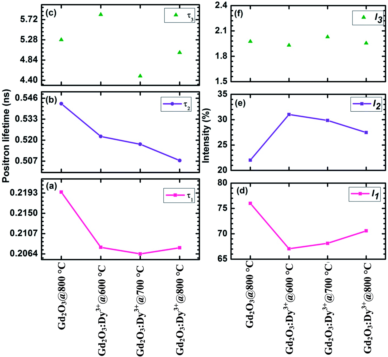 | ||
| Fig. 6 Positron lifetime (a) τ1 (b) τ2 (c) τ3 and intensity (d) I1 (b) I2 (c) I3 of Gd2O3 annealed at 800 °C and Gd2O3:Dy3+ annealed at different temperature. | ||
| Phosphors | Annealing temperature | τ1 (ns) | τ2 (ns) | τ3 (ns) | τav (ns) | I1 (%) | I2 (%) | I3 (%) |
|---|---|---|---|---|---|---|---|---|
| Gd2O3 | 800 °C | 0.220 | 0.543 | 5.281 | 0.292 | 75.996 | 22.029 | 1.975 |
| Gd2O3:Dy3+ | 600 °C | 0.208 | 0.522 | 5.830 | 0.307 | 67.052 | 31.018 | 1.930 |
| 700 °C | 0.206 | 0.518 | 4.492 | 0.301 | 68.12 | 29.851 | 2.029 | |
| 800 °C | 0.208 | 0.507 | 5.002 | 0.292 | 70.583 | 27.461 | 1.956 |
The first lifetime τ1 component of undoped Gd2O3 phosphor is approximately 0.22 ± 0.0013 ns and the corresponding intensity is approximately 76%. The observed value originate due to the annihilation of positrons at the grains, grain boundaries and their interface.37 Grain boundaries being rich in defects, act as strong trapping centres for positrons and a large fraction of positrons get trapped in the vicinity of grain boundaries rendering a few positrons to annihilate with free electrons inside a grain. In those cases, if the positron lifetime in the grain boundary defects is close to their free annihilation lifetime in defect free regions inside a grain, τ1 may represent a mixed lifetime comprising of both annihilation at grain, grain boundary and mono vacany in the crystallite as well. The intermediate lifetime τ2 = 0.54 ± 0.0051 ns, I2 = 22% is due to the defect species components originating from the annihilation of positron at vacancy clusters located within the grains.38 After thermalization, some positrons escape without annihilating at the grain boundaries and get trapped at the nanovoids (vacancy clusters).
On substituting Dy3+ in Gd3+ site and annealing at different temperatures affect the positron lifetime to a greater extent. It clearly reveals that the addition of Dy3+ in Gd2O3 induces more defects at the grain boundary as a result of increased electron density but decreases the τ1. In Gd2O3:Dy3+ annealed at different temperatures, τ1 value remains almost same and I1 varies gradually from 67% to 71%. During the synthesis, Dy3+ ions may get trapped at different locations either individually or forming a bulk clusters. When the phosphor is annealed at different temperatures, the Dy3+ ions start migrating and tend to occupy the voids in the matrix and so the electron density around the positron traps increases. As a result, τ2 and I2 value decrease with annealing temperatures. Thus, the annealing plays a significant role in reducing the vacancy defects and intensively affect the luminescence properties of Gd2O3:Dy3+ phosphor (explained in the next session).
The long lifetime τ3 is due to the formation of positronium by the positron trapped in large voids in the intercrystalline region of the nanoparticles.39 During the annealing process grain growth occurs through the intersection of grain with the neighbouring grain. The interfaces between the nearby grains are the site of very low electron density and it can act as favourable sites for the formation of positronium. In Gd2O3:Dy3+ annealed at 600 °C, some of the Dy3+ ions remains at the surface of the particle and at the intersection of grains. So the ortho-positronium formed in this region has lifetime of 5.83 ± 0.0657 ns and the average crystallite size estimated from XRD is 15 nm. Further on increasing the annealing temperature to 700 °C, grain growth reduces the free volume at the intersection of the grain and thereby increases the crystallite size to 33 nm and decreases the τ3 (4.492 ± 0.0571 ns) value. At 800 °C, free volume size increases owing to the growth on the boundary line (crystallite size – 44 nm) and hence decrease the electron density and its corresponding τ3 value increases to 5.002 ± 0.062 ns. The increase in free volume size may be due to the migration of Dy3+ ions at the interface. The annihilation of positron through the formation of ortho-positronium intensity (I3) is only around 2% for all the samples and therefore, the intensity has been excluded in the average lifetime calculation.
From Doppler broadening the S and W parameters covering the low and high momentum region40 are deduced for further investigation of defects. Fig. 7 represents the variation of S and W parameters of pure Gd2O3 annealed at 800 °C and Gd2O3:Dy3+ annealed at various temperature. S value dominates for Gd2O3:Dy3+ annealed at 600 °C due to the presence of large number of Dy3+ ions residing on the grain boundary sites. On further increasing the annealing temperature to 700 °C, the S parameter declines and the W-parameter attains a moderate value implying that the Dy3+ ions begin to migrate and occupy in the Gd3+ sites and thereby, reduce the defect concentration. When the phosphor is annealed at 800 °C, most of the Dy3+ ions occupy the Gd3+ site of Gd2O3 and hence, the value of S and W parameters shift towards the value of pure Gd2O3 annealed at 800 °C. The decrease in the S-parameter is certainly due to the reduction of vacancy clusters and the larger fractions of positrons annihilation in the bulk.
 | ||
| Fig. 7 S–W plot of Gd2O3 annealed at 800 °C and Gd2O3:Dy3+ annealed at different temperature. | ||
Fig. 8 shows the excitation spectra of Gd2O3:Dy3+ phosphors annealed at 600 °C, 700 °C and 800 °C and the phosphors are excited at 572 nm which is the major yellow emission wavelength of Dy3+ ions. All the spectra exhibit five distinct peaks at 230 nm, 274 nm, 313 nm, 350 nm and 384 nm with varying intensity. The strong peak at 230 nm denotes the host absorption band (HAB). The small shoulder peak at 256 nm, the intense narrow peak at 274 nm and weak peak at 313 nm correspond to the electron transition from 8S7/2 to 6DJ, 8S7/2 to 6IJ and 8S7/2 to 6PJ lying within the energy levels of Gd3+ respectively.41 The spectral peaks related to the intrinsic f–f transitions in the Dy3+ ions are present at 350 nm and 384 nm which is due to the transition from the ground state 6H15/2 to the excited state 6P7/2 and 4F7/2 respectively.15 From the excitation spectra, it can be observed that annealing the phosphor from 600 °C to 800 °C, the intensity of the peak increases due to the improved crystallinity of the phosphors and the presence of excitation peaks of Gd3+ in Dy3+ excitation spectra clearly reveals the energy transition from Gd3+ to Dy3+. The similar energy transfer peaks are observed in Gd(BO2)3:Dy3+ and in Gd3Al5O12:Dy3+ phosphor.15,42
 | ||
| Fig. 8 PL excitation spectra of Gd2O3:Dy3+ phosphors recorded at 572 nm. | ||
In order to investigate the energy transfer process, the emission spectra of Gd2O3:Dy3+ phosphors are monitored by exciting Gd3+ at 274 nm. In Fig. 9, the emission spectra include a strong yellow emission at 572 nm, blue emission at 486 nm, and a weak red emission at 669 nm (enlarged view is shown as an inset in Fig. 9) which are assigned to the energy transition from the excited state 4F9/2 to three different ground state 6H15/2, 6H13/2 and 6H11/2 respectively. In the electronic states of rare earth ions, magnetic and electric dipole transition occur predominantly where the former is allowed and the later is a forced transitions. Even though the electric dipole transition is forbidden, it occurs when rare earth ion occupies non-inversion symmetry site. In Dy3+, the emission peak at 486 nm (4F9/2–6H15/2) is an allowed magnetic dipole transition and is insensitive to the environment.10 The parity forbidden electric dipole transition at 572 nm (4F9/2–6H13/2) is hypersensitive and strongly affected by the ligand environment. The asymmetric ratio (R) is the integrated intensity ratio of 4F9/2–6H13/2 and 4F9/2–6H15/2 which is used to estimate the symmetry around the Dy3+ in the phosphor.43 The asymmetric ratio calculated for Gd2O3:Dy3+ phosphors annealed at 600 °C, 700 °C and 800 °C are 3.37, 3.21 and 3.26 respectively. All the values are in the order of 3 implying that the Dy3+ ions are located at the non-inversion symmetry site in Gd2O3. It is very interesting to note that from a single phosphor source it is possible to obtain three different emission colours like blue, yellow and red. The possible energy transfer process from Gd3+ to Dy3+ is schematically illustrated in the Fig. 10. On exciting the phosphor at 274 nm, 6IJ of Gd3+ is populated and further the energy is transferred to Dy3+ and emission occurs from 4F9/2.
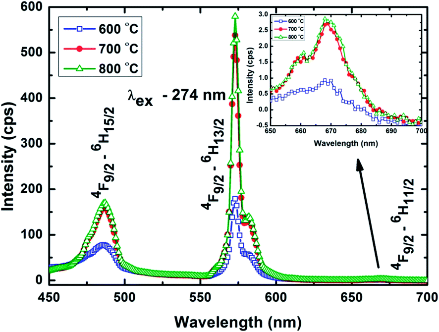 | ||
| Fig. 9 Emission spectra of Gd2O3:Dy3+ phosphors recorded at 274 nm. | ||
 | ||
| Fig. 10 Schematic representation of energy transfer process. | ||
Many literatures on phosphor have reported the presence of dominant yellow emission from Dy3+ occupying the non-inversion site in YAl3(BO3)4, SrSiO4 and GdAlO3.43–45 Similarly the dominant blue emission is observed for the Dy3+ ions occupying the inversion site in GdPO4, K2MgP2O7 and GdFeO3 phosphor.46–48 In case of Gd2O3, a sesquioxides with cubic bixbyite structure (Ia) have crystallographically two nonequivalent cationic sites with 6-fold coordination namely C2 non-inversion symmetry with Gd3+ in the centre of a distorted cube with two oxygen vacancies on the face diagonal and S6 site symmetry with inversion symmetry resulting from two oxygen vacancies lying on one body diagonal.49 The photoluminescence properties varies with the site preference. In Gd2O3, 75% Gd3+ ions occupy the C2 sites, and 25% Gd3+ ions occupy the S6 sites.50,51 Stanek et al. have reported the site preference of solute cation (here Dy3+) as a function of the ratio between solute and host lattice cation (here Gd3+). When the ratio is less than 1, most of the solute cation occupies C2 site and for value greater than 1, S6 site is preferred. In the present case, the ionic ratio is 0.972 and so Dy3+ prefers C2 site than S6.
The luminescence decay curve of Gd2O3:Dy3+ phosphor is presented in Fig. 11a–c. It is recorded for the dominating wavelength of 572 nm (4F9/2–6H13/2). The curves are fitted with bi-exponential decay presented in eqn (6).
| I = A1e−t/τ1 + A2e−t/τ2 | (6) |
 | ||
| Fig. 11 Luminescence decay curve of Gd2O3:Dy3+ annealed at (a) 600 °C (b) 700 °C (c) 800 °C. | ||
The influence of annealing temperature on defect concentration is estimated by comparing and relating the positron average lifetime, the values of S parameter, the yellow emission peak centred at 572 nm and fluorescence lifetime (refer Fig. 12). Upon annealing, the luminescence intensity and fluorescence lifetime τ2 increases (refer Fig. 12(a)) due to the reduction of lattice defects (refer Fig. 12(b)) which is evident from τav and S parameter of PALS.
 | ||
| Fig. 12 Comparison of (a) PL intensity of 572 nm and fluorescence lifetime τ2 (b) positron τav and S parameter as a function of annealing temperature. | ||
Further, to represent the predominant colour emission at each annealing temperature, a CIE (Commission International de I'Eclairage 1931) plot is plotted and depicted in Fig. 13. In this plot, at 600 °C, the emission intensities of blue and yellow are more or less same implying that an equal number of Dy3+ ions are substituted in the inversion and non-inversion symmetry site of Gd3+. The equal contribution from the blue emission and yellow emission tends to shift the CIE point close to the white region of the chromaticity coordinates. On further annealing the phosphor to 700 °C and 800 °C the blue emission gets suppressed and the yellow emission is enhanced. This is attributed to the non-uniform distribution of Dy3+ ions where the large fraction of the ions resides on the non-inversion symmetry site and thus, enhancing and shifting the CIE point towards the yellow region of the chromaticity coordinates. The shift and change in the emission colour are highly reflected in the CIE graph. Thus, by blending an appropriate composition of blue, yellow and red emission, a suitable white colour emission can be achieved in Gd2O3:Dy3+ phosphor which finds an intensive application in fabricating white LEDs. The CIE coordinates and the quantum yield as a function of annealing temperature are tabulated in the Table 3. The increase in quantum yield with the increase in annealing temperature well supports the fine substitution of Dy3+ ions in Gd2O3 matrix.
 | ||
| Fig. 13 CIE plot of Gd2O3:Dy3+ phosphors prepared at different annealing temperatures. | ||
| Annealing temperature | CIE coordinates | Quantum yield (%) | |
|---|---|---|---|
| x | y | ||
| 600 °C | 0.29 | 0.346 | 18.52 |
| 700 °C | 0.347 | 0.406 | 21.277 |
| 800 °C | 0.351 | 0.408 | 21.602 |
Conclusions
In summary, Gd2O3:Dy3+ is successfully synthesized by citrate-based sol–gel process. PALS shows annihilation of positron at various defects in the lattice like grain boundary defects, vacancy, voids and clusters. Positron lifetime studies indicate that the lattice defects created during the synthesis condition gets reduced on annealing. Under Gd3+ excitation at 273 nm, Gd2O3:Dy3+ phosphors exhibit characteristic transition peaks of Dy3+ at 486 nm, 572 nm and 669 nm. It clearly indicate a strong energy transfer process from Gd3+ to Dy3+. The theoretically predicted occupancy of Dy3+ ions at C2 site of Gd3+ is also proved experimentally. The luminescence decay value τ2 increases with temperature due to the reduction of defects and substitution of Dy3+ for Gd3+. On annealing the phosphors at different temperatures, the emission from Dy3+ is enhanced with the decrease in lattice defects. CIE coordinates proved that Gd2O3:Dy3+ can give a colour very close to the white light. It can also be tuned to emit blue or yellow colour based on the occupancy of Dy3+ in Gd3+ site.Acknowledgements
T. Selvalakshmi thank DST INSPIRE Fellowship (2011/297) New Delhi for the financial support. We would like to thank Dr S. Velmathi, Department of Chemistry, National Institute of Technology, Tiruchirappalli – 620015 for DRS and PL measurements and National Centre for Ultra Fast Processes, University of Madras, Chennai for Fluorescence lifetime measurement.References
- W.-R. Liu, C.-H. Huang, C.-W. Yeh, J.-C. Tsai, Y.-C. Chiu, Y.-T. Yeh and R.-S. Liu, Inorg. Chem., 2012, 51, 9636–9641 CrossRef CAS PubMed.
- J. A. Dorman, J. H. Choi, G. Kuzmanich and J. P. Chang, J. Phys. Chem. C, 2012, 116, 10333–10340 CAS.
- J. Chen, Q. Meng, P. S. May, M. T. Berry and C. Lin, J. Phys. Chem. C, 2013, 117, 5953–5962 CAS.
- Y. Pan, Q. Zhang, C. Zhao and Z. Jiang, Solid State Commun., 2007, 142, 24–27 CrossRef CAS PubMed.
- L. Wang and Y. Li, Chem. Mater., 2007, 19, 727–734 CrossRef CAS.
- W. Chen and A. Zhou, J. Phys. Chem. C, 2012, 116, 24748–24751 CAS.
- Z. Xia, J. Zhuang and L. Liao, Inorg. Chem., 2012, 51, 7202–7209 CrossRef CAS PubMed.
- C.-H. Huang, T.-S. Chan, W.-R. Liu, D.-Y. Wang, Y.-C. Chiu, Y.-T. Yeh and T.-M. Chen, J. Mater. Chem., 2012, 22, 20210–20216 RSC.
- E. Pavitra, G. Seeta Rama Raju, Y. H. Ko and J. S. Yu, Phys. Chem. Chem. Phys., 2012, 14, 11296–11307 RSC.
- Z.-W. Zhang, Z.-Y. Moa, S.-T. Song, J.-P. Zhang, L. Liu, W.-G. Zhang and D.-J. Wang, Mater. Lett., 2013, 90, 1–3 CrossRef CAS PubMed.
- X. Yu, L. Zhang, X. Xu, T. Wang, H. Yu, T. Jiang, Q. Jiao, Z. Yang, D. Zhou and J. Qiu, J. Lumin., 2014, 145, 114–118 CrossRef CAS PubMed.
- R.-Y. Yang and H.-L. Lai, J. Lumin., 2014, 145, 49–54 CrossRef CAS PubMed.
- P. V. Do, V. P. Tuyen, V. X. Quang, N. T. Thanh, V. T. T. Ha, H. V. Tuyen, N. M. Khaidukov, J. Marcazzó, Y.-I. Lee and B. T. Huy, Opt. Mater., 2013, 35, 1636–1641 CrossRef PubMed.
- B. P. Kore, N. S. Dhoble, S. P. Lochab and S. J. Dhoble, J. Lumin., 2014, 145, 299–306 CrossRef CAS PubMed.
- X. Zhang, F. Meng, W. Li, S. I. Kim, Y. M. Yu and H. J. Seo, J. Alloys Compd., 2013, 578, 72–76 CrossRef CAS PubMed.
- E. Pavitra, G. S. R. Raju and J. S. Yu, Ceram. Int., 2013, 39, 6319–6324 CrossRef CAS PubMed.
- Y.-H. Lin, M. Li, C.-W. Nan and Z. Zhang, J. Am. Ceram. Soc., 2007, 90, 2991–2994 Search PubMed.
- E. Kuramoto, T. Tsutsumi, K. Ueno, M. Ohmura and Y. Kamimura, Comput. Mater. Sci., 1999, 14, 28–35 CrossRef CAS.
- Z. Wang, Z. Q. Chen, J. Zhu, S. J. Wang and X. Guo, Radiat. Phys. Chem., 2000, 58, 697–701 CrossRef CAS.
- R. W. Siegel, Annu. Rev. Mater. Sci., 1980, 10, 393–425 CrossRef CAS.
- Z. Lu, L. Weng, S. Song, P. Zhang, Q. Hou and X. Ren, J. Sol-Gel Sci. Technol., 2012, 62, 160–169 CrossRef CAS.
- Y.-H. Lin, M. L. Li, C.-W. Nan and Z. Zhang, J. Am. Ceram. Soc., 2007, 90, 2992–2994 CrossRef CAS PubMed.
- A. V. Thorat, T. Ghoshal, J. D. Holmes, P. M. G. Nambissan and M. A. Morris, Nanoscale, 2014, 6, 608–615 RSC.
- J. Zhang, Z. Zhang, Z. Tang, Y. Tao and X. Long, Chem. Mater., 2002, 14, 3005–3008 CrossRef CAS.
- H. Saito and T. Hyodo, Radiat. Phys. Chem., 2003, 68, 431–434 CrossRef CAS.
- C. Suryanarayana and M. Grant Norton, X-ray diffraction-A practical approach, Plenum Press, New York, London, 1998, ch. 3, pp. 207–221 Search PubMed.
- J. Sivasankari, S. Sankar, S. Selvakumar, L. Vimaladevi and R. Kirthiga, Mater. Chem. Phys., 2014, 143, 1528–1535 CrossRef CAS PubMed.
- B. Smith, Infrared Spectral Interpretation-A Systematic Approach, CRC Press LLC, Florida, 1999, ch. 1, pp. 1–29 Search PubMed.
- R. Yogamalar, S. Anita, R. Srinivasan, A. Vinu, K. Ariga and A. C. Bose, J. Nanosci. Nanotechnol., 2009, 9, 5966–5972 CrossRef CAS PubMed.
- S. Lechevallier, P. Hammer, J. M. A. Caiut, S. Mazeres, R. Mauricot, M. Verelst, H. Dexpert, S. J. L. Ribeiro and J. Dexpert-Ghys, Langmuir, 2012, 28, 3962–3971 CrossRef CAS PubMed.
- Y. Jinqiu, C. Lei, H. Huaqiang, Y. Shihong, H. Yunsheng and W. Hao, J. Rare Earths, 2014, 32, 1–4 CrossRef.
- H. Guo, N. Dong, M. Yin, W. Zhang, L. Lou and S. Xia, J. Phys. Chem. B, 2004, 108, 19205–19209 CrossRef CAS.
- C. L. Luyer, A. G. -Murillo, E. Bernstein and J. Mugnier, J. Raman Spectrosc., 2004, 34, 234–239 CrossRef PubMed.
- W. A. Pisarski, T. Goryezka, J. Pisarska and W. R. -Romanowski, J. Phys. Chem. B, 2007, 111, 2427–2430 CrossRef CAS PubMed.
- M. L. Pang, J. Lin, J. Fu, R. B. Xing, C. X. Luo and Y. C. Han, Opt. Mater., 2003, 23, 547–558 CrossRef CAS.
- Z. Jiao, T. Chen, J. Xiong, T. Wang, G. Lu, J. Ye and Y. Bi, Nature, 2013, 3, 1–6 Search PubMed.
- T. E. M. Staab, R. K. -Rehberg and B. Kieback, J. Mater. Sci., 1999, 34, 3833–3851 CrossRef CAS.
- S. He, C. Li, H. Chen, D. Su, B. Zhang, X. Cao, B. Wang, M. Wei, D. G. Evans and X. Duan, Chem. Mater., 2013, 25, 1040–1046 CrossRef CAS.
- T. Ghoshal, S. Kar, S. Biswas, S. K. De and P. M. G. Nambissan, J. Phys. Chem. C, 2009, 113, 3419–3425 CAS.
- P. Parz, B. Fuchsbichler, S. Koller, B. Bitschnau, F.-A. Mautner, W. Puff and R. Wurschum, Appl. Phys. Lett., 2013, 102, 151901–151904 CrossRef PubMed.
- M. Jayaimhadri, B. V. Ratnam, K. Jang, H. S. Lee, B. Chen, S.-S. Yi, J.-H. Jeong and L. R. Moorthy, Int. J. Appl. Ceram. Technol., 2011, 8, 709–717 CrossRef PubMed.
- J. Li, J.-G. Li, S. Liu, X. Li, X. Sun and Y. Sakka, J. Mater. Chem. C, 2013, 1, 7614–7622 RSC.
- G. V. L. Reddy, L. R. Moorthy, B. C. Jamalaiah and T. Sasikala, Ceram. Int., 2010, 39, 2675–2682 CrossRef PubMed.
- S. K. Gupta, M. Kumar, V. Natarajan and S. V. Godbole, Opt. Mater., 2013, 35, 2320–2328 CrossRef CAS PubMed.
- G. S. R. Raju, J. Y. Park, H. C. Jung, H. K. Yang, B. K. Moon, J. H. Jeong and J. H. Kim, Opt. Mater., 2009, 31, 1210–1214 CrossRef PubMed.
- A. I. Becerro, S. R. -Liviano, A. J. F. -Carrion and M. Ocana, Cryst. Growth Des., 2013, 13, 526–535 CAS.
- R. L. Kohalea and S. J. Dhoble, J. Lumin., 2013, 138, 153–156 CrossRef PubMed.
- Y. Zhang, A. Zheng, X. Yang, H. He, Y. Fan and C. Yao, CrystEngComm, 2014, 14, 8432–8439 RSC.
- C. R. Stanek, K. J. McClellan, B. P. Uberuaga and K. E. Sickafus, Phys. Rev. B: Condens. Matter Mater. Phys., 2007, 75, 134101–134107 CrossRef.
- E. Antic-Findancev, J. Hosla and M. Lastusaari, J. Alloys Compd., 2002, 341, 82–86 CrossRef.
- E. Antic-Fidancev, J. Hölsä and M. Lastusaari, J. Phys.: Condens. Matter, 2002, 15, 863–876 CrossRef.
- A. I. Becerro, S. R. -Liviano, A. J. F. -Carrion and M. Ocana, Cryst. Growth Des., 2013, 13, 526–535 CAS.
- A. K. Parchur, A. I. Prasad, S. B. Rai, R. Tewari, R. K. Sahu, G. S. Okram, R. A. Singh and R. S. Ningthoujam, AIP Adv., 2012, 2, 032119 CrossRef PubMed.
| This journal is © The Royal Society of Chemistry 2014 |