Inkjet-printed PEDOT:PSS electrodes on plasma-modified PDMS nanocomposites: quantifying plasma treatment hardness

Alessandro Chiolerio*a, Paola Rivolob, Samuele Porroa, Stefano Stassiab, Serena Ricciardib, Pietro Mandraccib, Giancarlo Canavesea, Katarzyna Bejtkaa and Candido Fabrizio Pirriab
aCentre for Space Human Robotics, Istituto Italiano di Tecnologia, Corso Trento 21, 10129 Torino, Italy. E-mail: alessandro.chiolerio@iit.it
bApplied Science and Technology Department, Politecnico di Torino, Corso Duca degli Abruzzi 24, 10129 Torino, Italy

Received 9th July 2014 , Accepted 23rd September 2014

First published on 23rd September 2014


Abstract

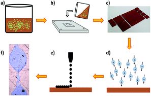
Nanostructured polymeric composites are promising materials for the fabrication of piezoresistive devices because they show a huge variation in electrical resistance when subjected to mechanical deformation. Quantum tunneling composites feature a conduction mechanism occurring between the metallic filler and copper particles embedded in a polydimethylsiloxane (PDMS) insulating matrix, and the mechanism is enhanced by the spiky morphology of the particles. PEDOT:PSS electrodes are patterned on either side of the composite by inkjet printing, a technology that allows one-step fabrication processes. The adhesion and spreading of conductive printed ink drops are controlled and enhanced by pre-treating the samples surface in an atmospheric pressure plasma customized system. Because of an extremely high metal to polymer ratio, which results in the different surface and dielectric properties of the composite, conventional plasma conditions are not suitable to allow the control of spreading. The optimal plasma conditions for ink/surface compatibility were found using quantitative comparison based on image analysis and numerical interpretation of the adhesion/roughness properties such as bulging and spread.


Introduction

Tactile sensing technology can be defined as the ability to transduce a given property of an object through physical contact with a sensing device.1 Nowadays, numerous techniques are available for the transduction of interface contact pressure or force between objects, which are described in several literature reviews on tactile sensing research. Most of these devices originate from biomedical and humanoid robot applications.1–5 Among all the possible working principles, only a few promising technologies are capable of fulfilling the requirements of these sensors for various applications. Currently, the most frequently used are capacitive and resistive sensors. The former is based on the change in capacitance between two parallel plates due to an externally induced deformation, while the latter is based on the resistance change of a piezoresistive layer when a deformation is applied.

Moreover, biomedical and robotic tactile sensors usually need to be flexible and adapt to the curvature of the host's structure and stretchable to cover joints and moving parts to correctly measure the interaction force.6

In previous experimental work we have reported various novel piezoresistive composites based on nanostructured metal fillers dispersed in a silicone matrix as functional material for tactile devices, in which the wide variation of piezoresistance achieved was attributed to quantum tunnelling conduction induced by the spiky particles covered by nanometric tips.7,8 Under un-deformed conditions, the composite material shows insulating behaviour, while after applying strain the electrical conductivity exponentially increases.9,10 In these composites, the conductive particles are separated from each other by a thin gap of insulating polymer, which represents the tunneling barrier. By applying a deformation to the sample, the thickness of the tunneling barrier is reduced, thus increasing the probability of tunneling phenomena and resulting in a huge reduction of the bulk electrical resistance.

Concerning the electrode deposition technique, literature reports several technologies and materials for flexible composites and rubber-based functional materials.11–13 Direct metal deposition allows the fabrication of very conductive electrodes and ensures very low contact resistance values; however, it suffers from a stiffness mismatch between the metallic electrodes and the polymer composite functional material. The differences in Young's modulus and elongation at break could induce the formation of a crack in the stiff electrode material during the stretching or bending of the device, consequently compromising electrical conduction. Moreover, the bonding force between the polymeric-based functional material and the metalized electrode film might be too weak to ensure good adhesion, and peeling off/detachment effects may occur.14–16 Because of an extremely high metal to polymer ratio, resulting in the different surface and dielectric properties of the composite, conventional plasma conditions are not suitable to allow control of spreading. To overcome these problems, this work reports the optimization of the direct printing of polymeric electrodes on the surface of plasma-treated composite materials.

Inkjet printing (IjP) is a versatile manufacturing technique for the direct deposition of electrical contacts on a variety of substrates.17 Several reviews on the new applications of IjP technology report the use of conductive inks based on metallic nanoparticles, which can either be dispersed in a carrier or generated in situ using a chemical reaction.18 Nanoparticle-based inks normally feature extremely high conductivities but require rather high temperatures for sinterization.19,20 Another possibility is represented by polymeric inks filled with graphene; however these are not yet suitable for practical applications as they feature high resistivities or require thermal sintering.21,22 More recently, inks based on conductive polymers were also developed.23 These are predominantly indicated for the fabrication of electrical patterns on substrates that cannot undergo thermal treatments, which is required for most inks based on metallic nanoparticles. In particular, inks based on poly(3,4-ethylenedioxythiophene):poly(styrenesulfonate) (PEDOT:PSS) were developed for this purpose because of their good solubility and ease of processing, and can be used as transparent, conductive coatings with high ductility.24

The adhesion of printed drops to the substrate is not only influenced by the rheological characteristics of the printed fluid, which can be adjusted before and during the printing process, but also by the physical and chemical properties of the substrates surface. PEDOT:PSS patterns show poor adhesion properties and imprecise geometry reproduction when printed on highly hydrophobic substrates such as polydimethylsiloxane (PDMS). Liquid spread is influenced by fluid properties, such as surface tension and viscosity, and by the relative surface energy and roughness of the substrate. Therefore, it is possible to limit and tune ink drops spread by carefully modifying the surface energy of the substrate.25 Moreover, surface morphology and modification can heavily impact the manner in which sessile drops deposit on a substrate by enhancing or limiting their coalescence.26

Surface modification techniques, such as wet chemical treatment, low pressure plasma treatment, and UV irradiation, have been widely applied to different substrates to enhance their adhesion properties and their applicability in functionalization processes.27,28 Among them, low pressure plasma treatments have been strongly exploited because they have been proven to be an effective way of modifying the surface of polymers. Many properties and functionalities can be obtained using plasma treatment, depending on the application: plasma can be used to tailor surface wettability, improve barrier characteristics, adhesion, dye-ability, printability, and oleophobicity.29 Chemical surface modification is initiated by a radical reaction between the plasma species and most of the external layers on the substrates surface, which occurs without the modification of bulk properties. In comparison to traditional low pressure plasma treatments, requiring high vacuum equipment or wet chemical treatments, which often involve the use of non-environmentally friendly chemicals and methods, plasmas operating at atmospheric pressure (APPs) offer an interesting alternative because of in-line process capabilities, relatively low costs, possible high throughput and low requirements of personal and environmental safety. In addition, non-thermal APPs usually work at temperatures in the range of 50–200 °C such that they can be safely employed for polymer modification. Several types of APPs operating in the regime of a non-thermodynamic equilibrium exist. Typical APP systems are corona discharges and dielectric barrier discharges (DBD).29,30 With the purpose of achieving a uniform surface treatment, plasmas homogeneous in time and space are desirable, although they are not always achievable with traditional corona discharges and DBDs. For instance, large plasmas were obtained using a series of individual discharges to form a larger array or using the DBD homogeneous mode, also called atmospheric pressure glow discharge (APG).31,32 This mode is characterized by the absence of streamers and the presence of a uniform glow, which is highly reminiscent of a low pressure glow discharge. Its selective characteristics can be adapted to a variety of treatments for various shapes and types of substrates.

In this work, an APP was tested for the surface modification of highly hydrophobic PDMS-based composite materials, containing a high volume fraction of metallic particles, whose presence causes a strong interaction of the material with the APP metallic electrodes. This procedure allowed the optimization of the surface properties of the composites for the deposition of PEDOT-PSS electrodes by inkjet printing.

Experimental

Piezoresistive nanocomposite preparation

The piezoresistive composite material was fabricated from bi-component polydimethylsiloxane (Dow Corning Corporation - SYLGARD 184) and nanostructured copper particles (POMETON Ltd. - LT10) presenting spiky tips on the surface with a technological flow process already described in previous works.7,8 The powder was dispersed in the PDMS base and after the addition of the PDMS curing agent, the blend was gently mixed to prevent tip smoothing and disruption. The resulting paste was poured into PMMA moulds, outgassed in vacuo and cured in oven at 70 °C for 3 h.

A sketch of the complete technological process starting from the preparation of the piezoresistive material up to the electrodes deposition is presented in Fig. 1.


image file: c4ra06878e-f1.tif
Fig. 1 Sketch of the technological process for the preparation of the piezoresistive composite. (a) Component mixing, (b) composite pouring, (c) demolding after the curing step, (d) plasma treatment, (e) inkjet printing and (f) the composite with PEDOT:PSS lines.

Atmospheric plasma system

The surface of the samples were treated using a DBD APP system (manufactured by ARIOLI S.p.A., Italy). The plasma discharge was lit on applying an RF bias in the 30–50 kHz frequency range between a metallic planar electrode covered by a polymeric dielectric layer and a plasma process tool. Two different types of plasma process tools were used, the first consisting of a set of stainless steel cylindrical electrodes, 30 cm in length, and the second consisting of a set of ceramic electrodes with a square cross section of the same length (detailed in Fig. 2a). The power applied to the plasma process tool was in the range of 400–550 W and 500–1100 W for the stainless steel and ceramic electrodes, respectively. Using the stainless steel tool, the maximum RF power that could be applied was limited by the interference between the metallic particles dispersed in the PDMS sample and the metal electrodes. This effect was reduced using the ceramic tool, allowing the application of high RF power to the samples. An Ar flow of 10 L min−1 was injected near the electrodes in order to displace the air and fill the plasma volume with Ar gas, thus allowing better control of the process atmosphere and improving the homogeneity of the plasma streamers. The treatments were applied moving the plasma process tool at a speed of 83 mm s−1 in a direction parallel to the samples, which were located on the planar dielectric layer. The vertical distance between the planar dielectric layer and the plasma process tool was varied in the range of 1.8–2.3 mm, depending on the sample thickness. Because of the possibility of moving the multi-electrode tool back and forth, different numbers of passes have been tested. The energy per unit area applied to the samples is calculated as Pn/(vl), where P is the power, n is the number of passes, v is the speed and l is the electrodes length, resulting in the range of 80–110 kJ m−2 for the metal tool and 100–220 kJ m−2 for the ceramic tool.
image file: c4ra06878e-f2.tif
Fig. 2 (a) Detailed schematic of the ceramic multi-electrode tool, where the high voltage connector (1), the insulation (2) and tube used to inject vaporized species (3) are shown; (b) picture of the active APP Ar glowing discharge using the ceramic multi-electrode.

Contact angle measurements

The effect of the surface plasma treatment was investigated using optical contact angle (OCA) measurements with an OCAH 200 instrument (DataPhysics Instruments GmbH) equipped with a CCD camera and an automatic dosing system for the liquid. Deionized water, MilliQ grade (H2O), and diiodomethane (CH2I2 – Sigma Aldrich) were used as liquids (droplet volume = 1.5 μL) for analysis according to the sessile droplet method in static mode. Datasets of liquid surface tension and dispersive/polar contributions for water and diiodomethane are γH2O = 72.8 mN, where γd = 21.8 mN m−1 and γp = 51.0 mN m−1 and γCH2I2 = 50.8 mN m−1, where γd = 48.5 mN m−1 and γp = 2.3 mN m.33,34 Drop profiles were fitted through the Young–Laplace method and contact angles between the fitted functions and base line were calculated using the SCA20 software.35 Standard deviation was calculated for each kind of sample on a data set of at least three droplets for each liquid. The surface free energy of both bare and plasma treated surfaces were determined through the Owens and Wendt method,36 according to the details reported in the ESI. To calculate these parameters, the contact angle of at least two liquids on the unknown solid was determined (water and diiodomethane in the present case).

Inkjet printing deposition of electrodes

PEDOT:PSS commercial ink (CleviosTM from Heraeus Precious Metals GmbH, Germany) was used as received. The ink was inserted into a 3 mL reservoir and loaded into the IjP system (JETLAB 4-XL from Microfab, US). The system was equipped with independent heaters for the printing nozzle and the substrate. Printing tests were achieved through piezoelectric nozzles made in quartz with diameter of 80 μm and a vibration frequency set to 500 Hz. The dimension and speed of ink drops were controlled by a horizontal camera located on the xy stage for direct drop observation. Jetting parameters were set as follows, using an asymmetrical pulse: first rise time of 3 μs, dwell time of 8 μs, fall time of 8 μs, echo time of 15 μs, second rise time of 3 μs, idle voltage of 3 V, dwell voltage of 35 V, echo voltage of −35 V. The nozzle was heated to a temperature of 40 °C to obtain the correct value of ink viscosity suitable for printing. Tracks with a length of 20 mm were printed by varying the resolution of the spotted ink droplets from 75 to 400 points per line (ppl) and varying the number of subsequent passes between 1 and 10, and then left to dry in air.

Morphological characterization

Morphological characterization of the untreated and plasma treated surface of the PDMS/Cu composites was performed by a field effect scanning electron microscope (FESEM, ZEISS Dual Beam Auriga). Track widths were measured and track morphology was determined under different printing parameter settings and various surface treatments using conventional optical microscopy (ZEISS AXIO). Optical microscope image analysis was performed using proprietary routines written in Matlab® M-script.

Electrical characterization

Functional characterization was performed on printed tracks using a standard 2-point micro-contact setup at room temperature, in a DC regime using a Keithley 2635A multimeter.37,38 Each sample has been measured using the same conditions three times to obtain sufficient data and process experimental points by computing the average and standard deviation.

Results and discussion

Contact angle analysis

The surface of the bare Cu microparticles–PDMS composite samples, 1 mm thick, was treated by an atmospheric pressure plasma customized system to enhance the controlled spreading of ink droplets and promote their coalescence. This was expected to improve the surface adhesion of the printed ink and ensure the continuity of conductivity for the device. Several process parameter permutations have been tested for both the types of electrode (metallic and ceramic), including RF power and number of passes to achieve a homogeneous discharge, approaching the condition of an atmospheric glow discharge on the exposed area and a quasi-permanent effect of treatment. Table 1 reports the contact angle analysis data (contact angle of both selected liquids and the surface free energy, together with dispersive and polar contributions) for the optimized process described in the experimental section, for the maximum applied RF power (1100 W) and 5 passes, by employing the ceramic multi-electrode tool and measuring the samples before and after the plasma process, both soon after the treatment and after aging for 2 h.
Table 1 Water and diiodomethane Optical Contact Angle (OCA) values and surface energy (SE) values divided in the polar and dispersive contributions of the untreated, treated and aged Cu microparticles–PDMS composites
Sample OCA PEDOT [°] OCA H2O [°] OCA CH2I2 [°] Surface energy [mN m−1] Dispersive component [mN m−1] Polar component [mN m−1]
Cu–PDMS 50 ± 1 122 ± 4 90 ± 1 13.0 13.0 0.0
Cu–PDMS after Ar-plasma 22 ± 1 16 ± 1 45 ± 2 70.0 22.2 47.8
Cu–PDMS after 2 h ageing post-plasma 28 ± 1 29 ± 4 49 ± 1 64.0 21.4 42.6


The Cu–PDMS composite shows the typical water contact angle of bare PDMS of about 120° suggesting that the metallic microparticles are confined in the bulk and do not affect the surface properties. Moreover, the surface energy of the sample is very low (13 mN m−1) because of its scarce interaction with diiodomethane, as reported for pure PDMS in ref. 39. The polar component of the diiodomethane surface tension cannot be ignored, thus preventing its spreading on the highly non-polar PDMS surface. A higher wettability could be reached only with non-polar liquids such as hexadecane (polar component of surface tension is equal to 0 mN m−1). The samples measured just after the plasma process show an abrupt decrease in the water contact angle (down to 16°) and an increase in surface energy (up to 70 mN m−1) typical of highly hydrophilic substrates. Both the polar and dispersive components are strongly modified by the treatment due to the strong oxidation on the surface as Ar plasma is activated in atmospheric air (the former), and structural changes in the PDMS polymeric surface chains (the latter), which are attributed to physical ablation performed by the discharge.40 The increased roughness and surface area, even though not visible to the naked eye, could improve the wettability by a non-polar liquid, such as diiodomethane, when compared with the poor spreading obtained on the untreated smooth substrate.41

Because surface energy may not be the only reason for the improved adhesion of the PEDOT ink after solvent evaporation, although it certainly affects its wettability when the ink is still in the liquid phase, we also evaluated the surface roughness before the plasma processing after the treatment and on aged samples. The images shown in Fig. 3 were used for the roughness evaluation, adapting them to run on a Matlab® routine previously developed to analyze particles and grains.42–44 The results reported in Table 2 indicate that roughness is doubled by the plasma treatment and is not affected by aging because it produces a physical modification of the composite.


image file: c4ra06878e-f3.tif
Fig. 3 FESEM analysis of the composite surface after plasma treatment with (a) metallic tool at 550 W (a deep damage of the surface, consistent with the appearance of erosion, is visible) and (b and c) ceramic tool at 1100 W. In (c) the inkjet printed PEDOT:PSS lines are visible. The scale bars correspond to 20 μm.
Table 2 Roughness of the untreated, treated and aged Cu microparticles–PDMS composites estimated according to a numerical algorithm based on the FESEM images (Fig. 3)
  Cu–PDMS Cu–PDMS after Ar-plasma Cu–PDMS after 2 h ageing post-plasma
Roughness [nm] 383 ± 300 716 ± 120 716 ± 120


The permanence of the effect of plasma treatment was studied by performing aging experiments. The contact angle analyses were repeated on the samples left for 2 h in air. Table 1 shows that the contact angles measured with the standard liquids are slightly affected by aging, resulting in a small decrease in the surface energy (64 mN m−1). Among the several attempted processes, only one (ceramic multi-electrode tool, power = 1100 W, 5 passes) achieved our non-trivial goal, such as a good compromise between the surface spreading enhancement, limited advantageous modification of surface roughness and permanence of the produced effects for a sufficiently time long to allow inkjet printing without the need of a multi-step implant. Considering that the PEDOT:PSS ink has a surface tension of 62 mN m−1 (reported in CleviosTM datasheet), a contact angle similar to water is expected.

It is worth noting that the ink shows a lower contact angle than water on the bare Cu–PDMS composite because of the presence of organic components that make it more compatible with the hydrophobic untreated polymeric surface. As expected, the plasma treatment produced a similar effect on both water and ink, and thus it can be inferred that the treatment acted on the aqueous component of the ink. The PEDOT:PSS wetting of the polymeric/metallic composite can be considered to be stable within 2 h after plasma modification. A longer storage time is known to lead to the recovery of the hydrophobic surface properties of pristine PDMS, even after an oxygen plasma treatment under vacuum.45 In the following paragraphs, it is demonstrated that a decrease of about 20° in the contact angle, i.e. 6 mN m−1 in surface energy, achieved a desirable spreading of ink drops, promoting liquid coalescence, and its adhesion was helped by the improved wettability of the surface. The fulfilment of these requirements is needed for the production of functional printed electrodes.

The best results of surface modification using the metallic electrode tool have been obtained using the 4 passes process at 550 W. The values of contact angle for water and diiodomethane are comparable. However, the use of this setup leads to a less homogenous discharge due to the formation of separated arcs. This possibly caused the motion of Cu microparticle clusters toward the surface, which resulted in the removal of material and the creation of holes and cracks on the surface of the composite. The result of this plasma treatment was clearly observed by FESEM analysis and a topographical view is shown in Fig. 3a. This phenomenon induces a modification of bulk composition in terms of micro-particles distribution that may negatively affect the piezoelectric device performance inducing the formation of electrically non-homogeneous clusters on the sample surface. These phenomena are considerably reduced when using the ceramic tool, which limits particle removal and surface damage, as is visible in Fig. 3b and c.

Analysis of inkjet printed electrodes on top of the composite

Fig. 4 shows a chromatically enhanced optical microscope image collection of PEDOT:PSS patterns printed on the PDMS/Cu composites before and after plasma treatment performed with the metallic tool. In particular, an array of straight lines was analyzed, composed of a number of droplets with a density in the range of 100–400 points per line (ppl). The analysis of the untreated surfaces confirms the poor wettability of the bare composite surface. On the other hand, it is possible to observe that bulging is induced on the liquid ink printed on the treated surfaces.46 This consists of a hydrodynamic instability producing regions that accumulate liquid subtracting it from other depleted regions, where the printed line is thinned and in some cases even interrupted. This phenomenon is more evident for the most energetic treatment (550 W for 4 passes) and for the pattern printed at a high resolution (400 ppl).
image file: c4ra06878e-f4.tif
Fig. 4 Collection of optical microscope images showing the surface of inkjet-printed tracks on the top of the PDMS/Cu composites. First row: untreated surfaces, 3 (a), 5 (b) and 10 (c) passes, printed tracks of a nominal width of 1 mm. Second row: printed tracks of a nominal width of 100 μm, after APP treatment with the metallic tool at 400 W, 3 passes, at 100 (d), 200 (e) and 400 (f) ppl. Third row: printed tracks of a nominal width of 100 μm, after APP treatment with the metallic tool at 550 W, 4 passes, at 100 (g), 200 (h) and 400 (i) ppl.

The bulging phenomenon may be controllable when the APP treatment is performed by the multi-electrode ceramic tool with plasma powers up to 1100 W. In the next paragraph, an operative procedure to correlate an engineering parameter (plasma hardness, defined further in the text) with post-printing features, such as good adhesion, bulging, etc., will be presented. We will see that a low hardness plasma treatment leads to a very low wetting, while a high one leads to high bulging.

The information content of each microscope image has been extracted by numerically assisted image analysis (IA) procedure, as shown for the composite in Fig. 5, where the first row sketches an example of the processing of a sample image, while the second row contains the data extracted from all the images taken on samples treated at 400 W using the metallic electrode. In particular, each histogram frame has been adjusted before conversion from RGB to 8-bit grayscale, and further posterized to a 2-bit valued B/W map (Fig. 5b); then a filter to detect the image edges was applied based on Sobel Gaussian computation. The resulting edge image (Fig. 5c) was imported in the Matlab® environment for statistical analysis. Each edge position, both the upper and lower, has been stored in a sequence of vectors (Fig. 5d) and further studied, extracting its mean edge position, standard deviation and so on. Each edge pixel, identified by a couple of values corresponding to its (x,y) coordinates, has been used to populate a statistic, which is limited to the y-position. Hence, the bin centre is the average y-position of the edge (zero) and the relative frequency is the number of pixels having a certain position over the total number of edge pixels (Fig. 5e). It is clear that a straight edge would result in monodisperse statistics with a very narrow peak centred at the mean value. Conversely, a bulging edge would result in a very disperse and broad peak, which is still centred at the mean value. When the periodicity of the bulging is such that in the same frame we can identify more than one ink circular area, a double peak broad distribution is found. For completeness, the experimental cumulative distribution is also given (Fig. 5f), showing perhaps the strongest evidence of the effects induced on the adhesion between ink and substrate by printing parameters, in this case the droplet density.


image file: c4ra06878e-f5.tif
Fig. 5 First row: image analysis procedure used to transform the optical microscope image of a printed track (a) into a 2-bit valued B/W map (b) and finally into a 2-bit valued map with edge evidence (c). Second row: the upper and lower profiles, as numerically extracted from the optical microscope imaging of samples treated with the metallic tool at 400 W under different printing conditions (d); the relative frequency plot of the edge statistics, obtained by normal Gaussian profile fitting (e); the cumulative frequency plot of the edge statistics (f).

Using the profiles represented in Fig. 5d we performed the following statistical analysis shown in the relative frequency plot of Fig. 5e. Three different printing densities (indicated as points per inch, ppi) result in three very different situations, where peak broadening is consistent with the occurrence of bulging from a straight line. On the x-axis, the bin centre is given in pixels; it is straightforward to see that increasing the IjP density, the printed area broadens and the excursion covered on the x-axis is greater. A slight asymmetry of the frequency profiles (horizontal shift with respect to zero) is due to the misalignment of line axis with respect to microscope frame axis but this un-compensated effect is not affecting the following discussion. The cumulative frequency plot of Fig. 5f compares the almost perfectly linear statistics of the sample printed at low density (straight line) with the other cases at a higher printing density, featuring a smoother distribution.

The results of the IA procedure are graphically presented in Fig. 6, showing the efficacy of our numerical procedure in classifying the different plasma treatments. Fig. 6a represents bulging broadness as a function of APP hardness, also giving information on the effective ink volumes as a colour scale (goal function). The plasma treatment hardness (engineering parameter) is defined as the APP power multiplied by the number of passes over the time elapsed because the treatment before IjP and the engineering volume is defined as the track density multiplied by the number of printing passes. Fig. 6a demonstrates that the phase space can be experimentally explored almost entirely by changing the process parameters. A low hardness plasma treatment results in a very low broadness/wetting of the surface, on low jetted volumes, while a high hardness plasma treatment leads results in high bulging broadness on almost every volume.


image file: c4ra06878e-f6.tif
Fig. 6 Peak #1 and peak #2 broadness (a) and R2 (b) as a function of the APP hardness, where each sample engineering volume has been represented in a colour scale; all experimental samples are reported.

Fig. 6b represents the Gaussian fit R2 to the relative probability (Fig. 5) as a function of APP hardness and effective volume: the higher this factor, the better the Gaussian fit. Note that there is no theory behind the choice of the Gaussian distribution other than its simplicity. When a simple criterion is applied with success, the corresponding process is also easily controlled. Depending on the relative probability distribution, single Gaussian or double Gaussian fits were performed. Both hard and soft APP treatments produce results whose statistics are not well represented by a simple Gaussian model, while mild treatments, those around 40 Js−2, are better described. The fill factor is defined as the number of pixels containing ink over the total number of pixels belonging to the area to be printed. This number has been computed only for the samples having a defined area to be printed (untreated substrate), while for the other samples, where line broadness results directly from droplet density and is not user-defined, we have given a fixed value of 1. Peak broadness is computed as the Gaussian fit peak width over its height. One of the key objectives of this study is to find an effective experimental procedure to limit ink consumption, and therefore the engineering volume should be as low as possible and the fill factor should be 1. We have observed that even a high number of passes (10) is not enough to approach these values, hence the necessity of an APP treatment. The fit is also useful for a quick evaluation of the fabrication procedure because its broadness should approach zero for perfectly straight lines without printing defects, while lines displaying bulging would result in a broader and double peak distribution.

Functional characterization

The electrical characteristics of the printed tracks were measured on the selected portions of the composite. Fig. 7a shows a typical response in the low voltage regime by contacting the composite sensing skin directly with tungsten micro-probes. The overall current flowing through the sample is low even though the experimental error is always kept well below 10% (red circles). When contacts are placed on the PEDOT:PSS printed tracks, the current flowing through the system is higher, more than doubled at positive potentials, but standard deviation is also increased, reaching up to 25% at positive potentials. This may also be due to plasma induced surface damage (Fig. 3a).
image file: c4ra06878e-f7.tif
Fig. 7 Two point IV curves acquired in the low (a) and high (b) voltage regime from the top surface of a piezoresistive Cu[thin space (1/6-em)]:[thin space (1/6-em)]PDMS sensor before and after (a), and after (b) the deposition of inkjet printed flexible polymeric electrodes.

This type of material is normally used under low voltage conditions because it is intended to be coupled to standard electronic devices (5 V) and low power energy sources.8 However, high electric field conditions were already used to induce the electric ageing of the nanocomposite samples in similar systems.47 Therefore, the high voltage regime was also investigated to potentially induce electromigration and exclude drifts in its response. Fig. 7b shows that in the high voltage regime our system after PEDOT:PSS printing saturates, the standard deviation may be as high as 100%. The saturation observed in the response indicates that there is no threshold for electromigration and that this noise is entirely due to instability toward high charge.

Conclusions

The optimization of an original process based on atmospheric pressure plasma treatment is described for improving the compatibility of an organic intrinsically conductive polymer with the hydrophobic surface of a composite material with an extremely high metal to polymer ratio is described. In particular, a composite piezoresistive artificial skin based on a matrix of PDMS and a dispersion of copper particles was tested. This process requires the use of an atmospheric pressure plasma treatment, which was tested using both metallic and ceramic RF electrode tools, resulting in several experimental values of damage on the surface of the polymer, contact angles, adhesion and spreading of the ink.

A novel procedure to quantify drop spreading was also developed based on optical microscope image analysis, and a numerical routine used to extrapolate the quantitative data from the bulging degree of the printed track profile. In addition, by quantifying the energy transferred to the substrate by means of the plasma treatment, it was possible to create a phase diagram, which was useful to understand and smartly classify optimal conditions for the improvement of compatibility. Electrical characterization was performed on untreated/treated samples after inkjet printing of electrodes, showing an improved signal and the absence of electromigration.

Notes and references

  1. M. H. Lee, Tactile sensing: new directions, new challenges, Int. J. Robot Res., 2000, 19(7), 636 Search PubMed.
  2. M. I. Tiwana, S. J. Redmond and N. H. Lovell, A review of tactile sensing technologies with applications in biomedical engineering, Sens. Actuators, A, 2012, 179, 17 CrossRef CAS PubMed.
  3. V. Maheshwari and R. Saraf, Tactile Devices To Sense Touch on a Par with a Human Finger, Angew. Chem., Int. Ed., 2008, 47(41), 7808 CrossRef CAS PubMed.
  4. H. Yousef, M. Boukallel and K. Althoefer, Tactile sensing for dexterous in-hand manipulation in robotics—A review, Sens. Actuators, A, 2011, 167(2), 171 CrossRef CAS PubMed.
  5. C. A. Bar, Evaluation of cushions using dynamic pressure measurement, Prosthet. Orthot. Int., 1991, 15(3), 232–240 CAS.
  6. V. Duchaine, N. Lauzier, M. Baril, M.-A. Lacasse and C. Gosselin, A Flexible Robot Skin for Safe Physical Human Robot Interaction, IEEE Int. Conf. Robot. Autom., 2009, 3676 Search PubMed.
  7. S. Stassi and G. Canavese, Spiky nanostructured metal particles as filler of polymeric composites showing tunable electrical conductivity, J. Polym. Sci., Part B: Polym. Phys., 2012, 50(14), 984 CrossRef CAS.
  8. T. Tommasi, A. Chiolerio, M. Crepaldi and D. Demarchi, A microbial fuel cell powering an all-digital piezoresistive wireless sensor system, Microsyst. Technol., 2014, 20, 1023–1033 CrossRef CAS.
  9. D. Bloor, K. Donnelly, P. J. Hands, P. Laughlin and D. Lussey, A metal–polymer composite with unusual properties, J. Phys. D: Appl. Phys., 2005, 38, 2851 CrossRef CAS.
  10. G. Canavese, M. Lombardi, S. Stassi and C. F. Pirri, Comprehensive characterization of large piezoresistive variation of Ni-PDMS composites, Appl. Mech. Mater., 2012, 110, 1336 Search PubMed.
  11. J. N. Patel, B. Kaminska, B. L. Gray and B. D. Gates, A Sacrificial SU-8 Mask for Direct Metallization on PDMS, J. Micromech. Microeng., 2009, 19, 115014 CrossRef.
  12. E. Buselli, A. M. Smith, L. M. Grover, A. Levi, R. Allman, V. Mattoli, A. Menciassi and L. Beccai, Development and characterization of a bio-hybrid skin-like stretchable electrode, Microelectron. Eng., 2011, 88, 1676–1680 CrossRef CAS PubMed.
  13. M. P. Chang and M. M. Maharbiz, Electrostatically-driven elastomer components for user-reconfigurable high density microfluidics, Lab Chip, 2009, 9, 1274–1281 RSC.
  14. C. Yu, Z. Wang, H. Yu and H. Jiang, A Stretchable Temperature Sensor Based on Elastically Buckled Thin Film Devices on Elastomeric Substrates, Appl. Phys. Lett., 2009, 95, 141912 CrossRef PubMed.
  15. A. Delcorte, S. Befahy, C. Poleunis, M. Troosters and P. Bertrand, Adhesion improvement for metallized silicone films, Adhes. Aspects Thin Films, 2004, 2, 1–12 Search PubMed.
  16. G. D. Sim, S. Won, C. Jin, I. Park, S. B. Lee and J. J. Vlassak, Improving the stretchability of as-deposited Ag coatings on poly-ethylene-terephthalate substrates through use of an acrylic primer, J. Appl. Phys., 2011, 109, 073511 CrossRef PubMed.
  17. H. Klauk, Plastic electronics: Remotely powered by printing, Nat. Mater., 2007, 6, 397 CrossRef CAS PubMed.
  18. M. Singh, H. M. Haverinen, P. Dhagat and E. G. Jabbour, Inkjet Printing—Process and Its Applications, Adv. Mater., 2010, 22, 673 CrossRef CAS PubMed.
  19. A. Chiolerio, G. Maccioni, P. Martino, M. Cotto, P. Pandolfi, P. Rivolo, S. Ferrero and L. Scaltrito, Inkjet printing and low power laser annealing of silver nanoparticle traces for the realization of low resistivity lines for flexible electronics, Microelectron. Eng., 2011, 88, 2481–2483 CrossRef CAS PubMed.
  20. A. Chiolerio, M. Cotto, P. Pandolfi, P. Martino, V. Camarchia, M. Pirola and G. Ghione, Ag nanoparticle-based inkjet printed planar transmission lines for RF and microwave applications: Considerations on ink composition, nanoparticle size distribution and sintering time, Microelectron. Eng., 2012, 97, 8–15 CrossRef CAS PubMed.
  21. R. Giardi, S. Porro, A. Chiolerio, E. Celasco and M. Sangermano, Inkjet printed acrylic formulations based on UV-reduced graphene oxide nanocomposites, J. Mater. Sci., 2013, 48, 1249–1255 CrossRef CAS.
  22. E. B. Secor, P. L. Prabhumirashi, K. Puntambekar, M. L. Geier and M. C. Hersam, Inkjet Printing of High Conductivity, Flexible Graphene Patterns, J. Phys. Chem. Lett., 2013, 4, 1347–1351 CrossRef CAS.
  23. B. J. De Gans, P. C. Duineveld and U. S. Schubert, Inkjet Printing of Polymers: State of the Art and Future Developments, Adv. Mater., 2004, 16, 203 CrossRef CAS.
  24. Z. Xiong and C. Liu, Optimization of inkjet printed PEDOT: PSS thin films through annealing processes, Org. Electron., 2012, 13, 1532 CrossRef CAS PubMed.
  25. F. Ely, C. O. Avellaneda, C. Molina, P. Paredez, V. C. Nogueira, T. E. A. Santos, V. P. Mammana, J. Brug, G. Gibson and L. Zhao, Patterning quality control of inkjet printed PEDOT: PSS films by wetting properties, Synth. Met., 2011, 161, 2129–2134 CrossRef CAS PubMed.
  26. P. J. Graham, M. M. Farhangi and A. Dolatabadi, Dynamics of droplet coalescence in response to increasing hydrophobicity, Phys. Fluids, 2012, 24, 112105-1–112105-20 Search PubMed.
  27. K. W. Lee, S. P. Kowalczyk and J. M. Shaw, Surface modification of BPDA-PDA polyimide, Langmuir, 1991, 7, 2450–2453 CrossRef CAS.
  28. J. Y. Zhang, H. Esrom, U. Kogelschartz and G. Eming, Modification of polymers with UV excimer Radiation form lasers and lamps, J. Adhes. Sci. Technol., 1994, 8, 1179–1210 CrossRef CAS PubMed.
  29. J. B. Park, J. S. Oh, E. L. Gil, S. J. Kyoung, J. T. Lim and G. Y. Yeoma, Polyimide Surface Treatment by Atmospheric Pressure Plasma for Metal Adhesion, J. Electrochem. Soc., 2010, 157(12), D614–D619 CrossRef CAS PubMed.
  30. M. Noeske, J. Degenhardt, S. Strudthoff and U. Lommatzsch, Plasma jet treatment of five polymers at atmospheric pressure: Surface modifications and the relevance for adhesion, Int. J. Adhes. Adhes., 2003, 24, 171–177 CrossRef PubMed.
  31. E. Kunhardt, Generation of large – volume, atmospheric- pressure nonequilibrium plasmas, IEEE Trans. Plasma Sci., 2000, 28(1), 189–200 CrossRef.
  32. S. Kanazawa, M. Kogoma, T. Moriwaki and S. Okzaki, Stable glow plasma at atmospheric pressure, J. Phys. D: Appl. Phys., 1988, 21, 838–840 CrossRef CAS.
  33. G. Ström, M. Fredriksson and P. Stenius, Contact Angles, Work of Adhesion, and Interfacial Tensions at a Dissolving Hydrocarbon Surface, J. Colloid Interface Sci., 1987, 119(2), 352–361 CrossRef.
  34. F. M. Fowkes, Attractive Forces at Interfaces, Ind. Eng. Chem., 1964, 56(12), 40–52 CrossRef CAS , Table VIII.
  35. F. K. Hansen, Surface tension by image analysis fast and automatic measurements of pendant and sessile drops and bubbles, J. Colloid Interface Sci., 1993, 160, 209–217 CrossRef CAS.
  36. D. K. Owens and R. C. Wendt, Estimation of the surface free energy of polymers, J. Appl. Polym. Sci., 1969, 13, 1741–1747 CrossRef CAS .Refrository Exact.
  37. S. Bocchini, A. Chiolerio, S. Porro, D. Accardo, N. Garino, K. Bejtka, D. Perrone and C. F. Pirri, Synthesis of polyaniline-based inks, doping thereof and test device printing towards electronic applications, J. Mater. Chem. C, 2013, 1, 5101 RSC.
  38. A. Chiolerio, S. Bocchini and S. Porro, Inkjet printed negative supercapacitors: synthesis of polyaniline-based inks, doping agent effect, and advanced electronic devices applications, Adv. Funct. Mater., 2014, 24, 3375–3383 CrossRef CAS.
  39. A. Lamberti, M. Quaglio, A. Sacco, M. Cocuzza and C. F. Pirri, Surface energy tailoring of glass by contact printed PDMS, Appl. Surf. Sci., 2012, 258, 9427–9431 CrossRef CAS PubMed.
  40. H. T. Kim and O. C. Jeong, PDMS surface modification using atmospheric pressure plasma, Microelectron. Eng., 2011, 88, 2281–2285 CrossRef CAS PubMed.
  41. M. Ramiasa, J. Ralston, R. Fetzer and R. Sedev, The influence of topography on dynamic wetting, Adv. Colloid Interface Sci., 2013, 206, 275–293 CrossRef PubMed.
  42. A. Chiolerio, M. Cotto, P. Pandolfi, P. Martino, V. Camarchia, M. Pirola and G. Ghione, Ag nanoparticle-based inkjet printed planar transmission lines for RF and microwave applications: considerations on ink composition, nanoparticle size distribution and sintering time, Microelectron. Eng., 2012, 97, 8–15 CrossRef CAS PubMed.
  43. A. Virga, P. Rivolo, E. Descrovi, A. Chiolerio, G. Digregorio, F. Frascella, M. Soster, F. Bussolino, S. Marchiò, F. Geobaldo and F. Giorgis, SERS active Ag nanoparticles in mesoporous silicon: detection of organic molecules and peptide-antibody assays, J. Raman Spectrosc., 2012, 43, 730–736 CrossRef CAS.
  44. A. Chiolerio, A. Virga, P. Pandolfi, P. Martino, P. Rivolo, F. Geobaldo and F. Giorgis, Direct patterning of silver particles on porous silicon by inkjet printing of a silver salt via in-situ reduction, Nanoscale Res. Lett., 2012, 7, 502 CrossRef PubMed.
  45. D. Bodas and C. Khan-Malek, Hydrophilization and hydrophobic recovery of PDMS by oxygen plasma and chemical treatment—An SEM investigation, Sens. Actuators, B, 2007, 123, 368–373 CrossRef CAS PubMed.
  46. D. Soltman and V. Subramanian, Inkjet-Printed Line Morphologies and Temperature Control of the Coffee Ring Effect, Langmuir, 2008, 24, 2224–2231 CrossRef CAS PubMed.
  47. A. Chiolerio, L. Vescovo and M. Sangermano, Conductive UV-cured acrylic inks for resistor fabrication: models for their electrical properties, Macromol. Chem. Phys., 2010, 211, 2008–2016 CrossRef CAS.

Footnote

Electronic supplementary information (ESI) available. See DOI: 10.1039/c4ra06878e

This journal is © The Royal Society of Chemistry 2014