
Electronic structure and optical properties of Si–O–N compounds with different crystal structures
Zhi-Gang Duanac,
Zong-Yan Zhao*a and
Pei-Zhi Yang*b
aFaculty of Materials Science and Engineering, Key Laboratory of Advanced Materials of Yunnan Province, Kunming University of Science and Technology, Kunming 650093, People's Republic of China. E-mail: zzy@kmust.edu.cn; Fax: +86-871-65107922; Tel: +86-871-65109952
bKey Laboratory of Advanced Technique & Preparation for Renewable Energy Materials, Ministry of Education, Yunnan Normal University, Kunming 650092, People's Republic of China. E-mail: pzhyang@hotmail.com
cCollege of Science, Southwest Forestry University, Kunming 650224, People's Republic of China
First published on 5th August 2014
Abstract
In order to explore the relationship between crystal structure and optical properties, five Si–O–N compounds with different crystal structures, including: α-quartz SiO2, β-quartz SiO2, Si2N2O, α-Si3N4, β-Si3N4 were considered in the present work. Using density functional theory with the GGA+U method, their crystal structure, electronic structure, and optical properties have been systematically investigated. The electronic structure of α and β phases of SiO2 (or Si3N4) are similar, but with some subtle differences that can be attributed to the different local bonding structure, and the electronic structure of Si2N2O shows the fundamental features of the electronic properties of SiO2 and Si3N4. Based on the calculated results, it is found that the optical properties not only are determined by the components of the Si–O–N compounds, but also are determined by the microstructure of the Si–O–N compounds. These calculated results will be useful as reference data for analyzing the optical properties of more complicated SiOxNy compounds. According to this principle, one could design novel Si–O–N compounds for specific optoelectronic applications, via tuning the composition and crystal structure.
1. Introduction
Silicon–nitrogen–oxygen compounds, including: silicon dioxide (silica, SiO2), silicon nitride (Si3N4), silicon oxynitride (Si2N2O), SiOxNy, etc., are important versatile functional materials. SiO2 is most commonly found in nature as quartz, and its applications range from structural materials to microelectronics to components used in the food industry (for example, ceramic, glass, optical fiber, refractory material, and so on). Owing to its several advantages: small linear expansion coefficient, good thermal shock resistance, low dielectric constant or thermal conductivity, simple production process, and low-cost, SiO2 becomes more and more very important material for current electronic industry.1 Si3N4 is high strength material (especially, the hot pressed Si3N4 is one of the world's hardest materials). Its strength can be maintained at the high temperature of 1200 °C without declining. At the same time, it has amazing resistance to chemical corrosion, and is a kind of high performance electrical insulating materials. During the past years, most of the considerable development work on Si3N4 has been conducted, primarily by the ceramics and electronic communities.2 Si2N2O is a stable compound in the Si3N4–SiO2 system, which has the transition structure between Si3N4 and SiO2. It is a strong covalent compound with a low density, high hardness, and has the advantages of thermal shock resistance, antioxidant, and thermodynamic stability. Thus, Si2N2O is a kind of very promising high-temperature structural material.3 SiOxNy is a very important material for optoelectronic applications, owing to the possibility of tailoring its electronic structure and optical properties by its elemental composition.4,5 For example, the amorphous thermal gate silicon dioxide (SiO2) should be replaced by amorphous SiOxNy to meet the challenge of nanoscale MOS devices, in which the gate dielectric thickness will be further scaled down to less than 4 nm.6SiOxNy compound with excellent properties of both SiO2 and Si3N4 compounds, has received the extensive concern. As a kind of similar to the valence bond structure of Si3N4 compound, SiOxNy processes particular chemical bond diversity and structural diversity, which determines its unique mechanics and thermodynamics properties of mechanics and thermodynamics (including: low density, high hardness, low thermal expansion coefficient, etc.). At high temperature of 1600 °C, SiOxNy still maintained good antioxidation properties. And, at high temperature of 1400 °C, its bending strength will not be significantly reduced. In recent years, SiOxNy film has been an important application in the field of microelectronics, is expected to replace thermal oxidation of SiO2 as the gate material, which can improve the dielectric constant, the ability to prevent the impurity diffusion, and radiation resistance.7 At the same time, SiOxNy thin films were also studied in the field of integrated optics. The refractive index and the extinction coefficient of SiOxNy thin films could be tuned by changing component proportion, resulting in applications of optical waveguide materials,8,9 gradient index thin films,10 and antireflection film. This character provides more facility for the integrated optical design. In addition, SiOxNy thin films can be used as silicon based light emitting materials.11
In the applications of solar cells, photodetectors, and photodiodes, the light trapping capability is one of the critical issues to improve the optoelectronic performance.12,13 In order to enhance the light trapping capability, researchers used SiOxNy thin films as anti-reflective coating on the front side of the devices to reduce the light reflectance. Compared with SiO2 component, the nitrogen component could change the dielectric constant of SiOxNy compound, because of the variation of the ionic polarizability.14 Recently, Qiu et al. proposed and fabricated quasi gradient index distribution of amorphous Si, SiNx, SiOxNy, and SiO2 stacks by plasma enhanced chemical vapor deposition and got a low average reflectance of 2–4.3% from 280–3300 nm wavelength.4,15 In fact, these optoelectronic applications are determined by its optical properties, such as dielectric function, refractive index, reflectivity, and so on. SiOxNy could break the dielectric breakdown of SiO2 layers of 1–2 nm thickness, at the same time preserve the excellent features (high thermal stability and high electron mobility) of SiO2.16,17 SiOxNy is transparent in the visible-light range and its refractive index can be varied from one of the SiO2 (∼1.44) to that of Si3N4 (∼2.02) by only acting on the oxygen and nitrogen concentrations, as well as its band gap could be increased by increasing the oxygen amount.7,18 Rebib et al. obtained SiOxNy layers with a large stoichiometry variation by the sputtering process of a pure silicon target under argon–oxygen–nitrogen atmosphere, and found that the refractive index of SiOxNy decrease linearly from 1.94 to 1.46 when the composition varies between Si3N4 and SiO2.19,20
Although, there are a lot of published works concerned the composition, properties, and performance of SiOxNy compounds. However, the most important aspects about the fundamental properties transition from SiO2, to Si2N2O, to SiOxNy, and to Si3N4, are still lacking at present. In order to further improve the fundamental understanding of SiOxNy compound, and provide helpful information about the relationship between electronic structure and optical properties, we chosen five crystal structures of Si–O–N compounds (including: α-quartz SiO2, β-quartz SiO2, Si2N2O, α-Si3N4, β-Si3N4) as research object, and adopted density functional theory (DFT) calculations as research method to investigate their electronic structure and optical properties, in the present work. These calculated results will be useful as reference data for analyzing the optical properties of more complicated SiOxNy compounds.
2. Computational methods
In the present work, all of the calculations were carried out by using the periodic density functional theory package of Cambridge Serial Total Energy Package (CASTEP) codes.21 CASTEP is a state-of-the-art quantum mechanics-based program designed specifically for solid-state materials science. The core electrons (Si: [Ne], O: [He], N: [He]) were treated with the ultrasoft pseudopotential. The exchange-correlation effects of valence electrons (Si: 3s23p2, O: 2s22p4, N: 2s22p3) were described by the revised Perdew–Burke–Ernzerhof for solid (PBEsol) of generalized gradient approximation (GGA).22 In order to obtain accurate electronic structure, the method of GGA+U was adopted to overcome the well-known shortcoming of GGA method.23 The Hubbard model is one of the most successful models to describe the correlated electrons in solids. In the present work, the U value of Si (O, and N)-p orbital was set as follows: Ueff = U − J = 7.90 eV, which is obtained by comparing the theoretical calculated and experimental measured band gap of crystal α-quartz SiO2. The Monkhorst–Pack scheme K-points grid sampling was set as 4 × 4 × 2 for the irreducible Brillouin zone. A 60 × 60 × 80 mesh was used for fast Fourier transformation. An energy cutoff of 380 eV was used for expanding the Kohn–Sham wave functions. The minimization algorithm was chosen the Broyden–Fletcher–Goldfarb–Shanno (BFGS) scheme.24 Its convergence criteria were set as follows: the force on the atoms were less than 0.03 eV Å−1, the stress on the atoms were less than 0.05 GPa, the atomic displacement was less than 1 × 10⁻³ Å, and the energy change per atom was less than 1 × 10⁻⁵ eV. Based on the optimized crystal structure, the electronic structure and the optical properties were then calculated.3. Results and discussions
3.1 Crystal structure
The five crystal structures of Si–O–N compounds are illustrated in Fig. 1. The coordination number of Si–O–N compounds is 4 for Si atoms, 3 for N atoms, and 2 for O atoms. α-quartz SiO2 has a trigonal structure with space group of P3121 (no. 152) and local symmetry D34; β-quartz SiO2 has a hexagonal structure with space group of P6222 (no. 180) and local symmetry D64. Their structures are known to have rather regular or slightly distorted [SiO4] tetrahedron link together at the corners in forming a network structure. The difference between α-quartz SiO2 and β-quartz SiO2 is that the six-membered ring structure is different in these two crystal structure: the Si–O bonds are unequal with two types of bond lengths (1.6166 and 1.6194 Å) in α-quartz SiO2; while the Si–O bonds are equal with bond length of 1.6144 Å in β-quartz SiO2. In the present work, the lattice constants of α-quartz SiO2 are obtained as: a = 4.9998 Å, c = 5.4934 Å, which is very consistent with experimental measurement:25 a = 4.913 Å, c = 5.405 Å; while the lattice constants of β-quartz SiO2 are obtained as: a = 5.0818 Å, c = 5.5668 Å, which is very consistent with experimental measurement:25 a = 5.01 Å, c = 5.47 Å. | ||
| Fig. 1 The crystal models of Si–O–N compounds in different crystal structures. The red balls represent oxygen atoms, the blue balls represent nitrogen atoms, and the gold balls represent silicon atoms. | ||
Si2N2O is the stable intermediate compound for the SiO2–Si3N4 compound system, resulting in its transition crystal structure between SiO2 crystal structure and Si3N4 crystal structure. It has an orthorhombic structure with space group of Cmc21 (no. 36) and local symmetry C2v12. The tetrahedron of [SiN3O] is connected with each others via shared vertices. In Si2N2O crystal structure, there three kinds of silicon atom ring structure: three-, four-, and six-membered ring. The three-membered ring is on the (100) plane, the four-membered ring is on the (011) plane, and the six-membered ring is on the (001) plane. The lattice constants of Si2N2O are: a = 8.932 Å, b = 5.525 Å, c = 4.870 Å, which are very closely with experimental measurement:26 a = 8.843 Å, b = 5.473 Å, c = 4.835 Å.
α-Si3N4 has a trigonal structure with space group of P31c (no. 159) and local symmetry C4v4; β-Si3N4 has a hexagonal structure with space group of P63/m (no. 176) and local symmetry C6h2. The tetrahedron of [SiN4] is connected with each others via shared vertices to form the three-dimensional network. There is only three-membered ring in the α-Si3N4 structure, while there are three- and four-membered rings in the β-Si3N4 structure. In the present work, the lattice constants of α-Si3N4 are obtained as: a = b = 7.783 Å, c = 5.641 Å, which is very consistent with previous calculated results:27 a = b= 7.766 Å, c = 5.615 Å; while the lattice constants of β-Si3N4 are obtained as:27 a = b = 7.635 Å, c = 2.915 Å, which is very consistent with previous calculated results: a = b = 7.586 Å, c = 2.902 Å.
All the crystal lattice parameters for these five Si–O–N compounds are tabulated in Table 1, which are well consistent with experimental data, indicating that the calculation methods in the present work are reasonable. Compared the crystal structures of α-SiO2 and β-SiO2, one could find that the symmetry of β-SiO2 is higher than the symmetry of α-SiO2, which is mainly exhibited by the rather regular [SiO4] tetrahedron in α-SiO2 structure and slightly distorted [SiO4] tetrahedron in β-SiO2 structure. The similar phenomenon could be found for α-Si3N4 and β-Si3N4: there are two different kinds of [SiN4] tetrahedra in α-Si3N4 structure (in which every Si–O band length or every N–Si–N band angle is different from one another, implying the four nitrogen atoms are completely unequal); while only one kind of [SiN4] tetrahedron in β-Si3N4 structure (in which two Si–O bonds are equal, and there are only two kinds of N–Si–N bond angle distribution). So, the symmetry of β-Si3N4 is higher than the symmetry of α-Si3N4. As the transition structure from SiO2 to Si3N4, Si2N2O structure has lower symmetry, obviously distorted [SiN3O] tetrahedron, and more complicated distribution of bond lengths or bond angles. The bond angle of Si–O–Si or Si–N–Si reflects the connection mode of tetrahedrons for these Si–O–N compounds. As shown in Table 1, there is only one connection mode between tetrahedrons in both SiO2 structures, four connection modes between tetrahedrons in Si2N2O structure; eight connection modes between tetrahedrons in α-Si3N4 structure; three connection modes between tetrahedrons in β-Si3N4 structure. These crystal lattice parameters indicate that the symmetry of microstructure for atomic bonding in α-Si3N4 structure is very lower, although its macro-symmetry is higher than that of Si2N2O structure.
| α-SiO2 | β-SiO2 | Si2N2O | α-Si3N4 | β-Si3N4 | ||
|---|---|---|---|---|---|---|
| a This bond angle is of O–Si–N. | ||||||
| Symmetry | Trigonal | Hexagonal | Orthorhombic | Trigonal | Hexagonal | |
| P3121 (D34, no. 152) | P6222 (D64, no. 180) | Cmc21 (C2v12, no. 36) | P31c (C4v4, no. 159) | P63/m (C6h2, no. 176) | ||
| Lattice constant | a = b = 5.001 Å, c = 5.494 Å, α = β = 90°, γ = 120° | a = b= 5.082 Å, c = 5.567 Å, α = β = 90°, γ = 120° | a = 8.932 Å, b = 5.525 Å, c = 4.870 Å, α = β = γ = 90° | a = b = 7.783 Å, c = 5.641 Å, α = β = 90°, γ = 120° | a = b = 7.635 Å, c = 2.915 Å, α = β = 90°, γ = 120° | |
| Crystal volume/molecule Å3 | 39.6667 | 41.4997 | 60.0843 | 73.985 | 73.568 | |
| Density/g cm−3 | 2.515 | 2.404 | 2.769 | 3.149 | 3.166 | |
| Binding energy/eV atom−1 | 8.303 | 8.300 | 8.546 | 8.613 | 8.613 | |
| Bond length/Å | Si–O | 1.6165, 1.6194 | 1.6144 | 1.6295 | ||
| Si–N | 1.7272, 1.7293, 1.7351 | 1.7275, 1.7341, 1.7374, 1.7416; 1.7440, 1.7456, 1.7504, 1.7556 | 1.7355, 1.7425, 1.7427 | |||
| Bond angle/degree | O–Si–O | 109.154, 110.489 | 107.970, 109.843 | 108.233a, 108.546a | ||
| Si–O–Si | 147.406 | 154.038 | 151.510 | |||
| N–Si–N | 107.415, 111.752 | 104.211, 108.710, 111.206, 112.905; 106.346, 108.710, 111.068, 114.372 | 108.009, 110.259 | |||
| Si–N–Si | 116.880, 118.695, 123.802 | 116.799; 117.254, 117.381, 122.859; 113.081, 120.255, 126.374; 119.999 | 113.542, 123.121; 120.000 | |||
| Net change/e | Si | 2.35 | 2.37 | 1.99 | 1.81, 1.82 | 1.83 |
| O | −1.18 | −1.18 | −1.43 | |||
| N | −1.12 | −1.36, −1.38 | −1.37, −1.38 | |||
| Si–O | 0.53 | 0.53 | 0.56 | |||
| Si–N | 0.61, 0.67, 0.66 | 0.68, 0.67, 0.69, 0.68, 0.69, 0.67, 0.63, 0.65 | 0.62, 1.39, 0.58 | |||
3.2 Electronic structure
The band structures of these five Si–O–N compounds are illustrated in Fig. 2. For α-SiO2, the valence band maximum (VBM) is located at the K k-point, while the conduction band minimum (CBM) is located at the Γ k-point, which means α-SiO2 is an indirect band gap semiconductor. The calculated band gap, the distance between VBM and CBM, is 8.702 eV, which is very consistent with experimental measurement (Eg = ∼8.7 eV),28 and larger and more accurate than that of previously reported band gap by theoretical calculations.27,29 The band gap of β-SiO2 (8.562 eV) is smaller than that of α-SiO2, and also belongs to an indirect band gap semiconductor (the VBM is located at M k-point, while the CBM is located at the Γ k-point). In the present work, we found that the spin up states and the spin down states are completely coincident, owing to the pairing electrons in all these five Si–O–N compounds. Thus, for the band structure in Fig. 2, the lines of spin up states are completely overlapping on the lines of spin down states. In the case of Si2N2O, the VBM is located at located at the Γ k-point, as well as the CBM. So, the band gap of Si2N2O, 7.729 eV, belongs to the direct band gap. For α-Si3N4, the VBM is located at M k-point, while the CBM is located at the Γ k-point. And the indirect band gap is 6.416 eV. In the case of β-Si3N4, the VBM is located at the k-point of Γ → A line, while the CBM is located at the Γ k-point. And the indirect band gap is 6.160 eV. As shown in Table 2, the direct band gaps are slightly larger than the minimum band gaps as discussed above, except α-SiO2. This situation leads to difficult or certain confusion for the band gap measurement in the practice.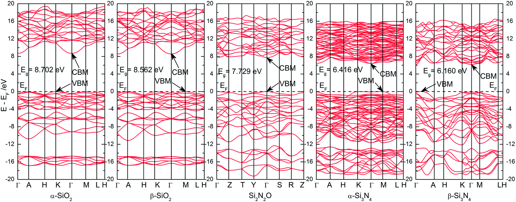 | ||
| Fig. 2 The calculated band structure of Si–O–N compounds in different crystal structures. The blue lines represent spin-up states, and the red lines represent spin-down states. Owing to the spin up states and the spin down states of these Si–O–N compounds are completely coincident, the blue lines of spin up states are completely overlapping on the red lines of spin down states. | ||
| α-SiO2 | β-SiO2 | Si2N2O | α-Si3N4 | β-Si3N4 | |
|---|---|---|---|---|---|
| Top of VB | K | M | Γ | M | Γ → A |
| Bottom of CB | Γ | Γ | Γ | Γ | Γ |
| Eg (minimum)/eV | 8.702 | 8.652 | 7.729 | 6.416 | 6.160 |
| Eg (direct at Γ)/eV | 9.167 | 8.791 | 7.729 | 6.486 | 6.292 |
| VB width/eV | 10.756 | 11.133 | 11.456 | 11.664 | 12.130 |
| CB width/eV | 10.730 | 10.574 | 9.585 | 9.572 | 9.320 |
| O 2s-band-width/eV | 2.150 | 2.011 | ∼2.573 | ||
| N 2s-band-width/eV | ∼3.935 | 6.294 | 6.123 |
The parameters of band structure of these five Si–O–N compounds are listed in Table 2. From SiO2 to Si2N2O and to Si3N4, as the oxygen component is gradually replaced by nitrogen component, the band gap (include the minimum band gap and the direct band gap at Γ k-point) is also gradually narrowing. The same or opposite variation tendency could be found for the band width variation of conduction band (CB) or valence band (VB). Because of the higher symmetry of β-SiO2 structure, the O-2s states related band width is relatively concentrated. Based on the same reason, the N-2s states related band width is also relatively concentrated in β-Si3N4 structure. Another important parameter for optoelectronics applications is the effective mass of carriers on the top of VB or on the bottom of CB. In order to further compare the electronic properties of these Si–O–N compounds, the effective mass of holes on the top of VB and electrons on the bottom of CB along the different directions are calculated by fitting the extreme point of E(k)–k relationship based on the band structures. The fitting results are illustrated in Table 3. The noticeable feature of the effective mass of carriers is anisotropic for all the five Si–O–N compounds. The minimum of hole effective mass for these five Si–O–N compounds is 0.198 m0 on A k-point along the direction of [00![[1 with combining macron]](https://www.rsc.org/images/entities/char_0031_0304.gif) ] (A → Γ) of β-SiO2 structure, and the minimum of electron effective mass for these five Si–O–N compounds is 0.205 m0 on Γ k-point along the direction of [001] (Γ → A) of β-Si3N4 structure. The present electronic structure and the corresponding parameters repeated the main features of Si–O–N compounds reported in previous literatures, but are more accurate than the earlier calculations.27–31
] (A → Γ) of β-SiO2 structure, and the minimum of electron effective mass for these five Si–O–N compounds is 0.205 m0 on Γ k-point along the direction of [001] (Γ → A) of β-Si3N4 structure. The present electronic structure and the corresponding parameters repeated the main features of Si–O–N compounds reported in previous literatures, but are more accurate than the earlier calculations.27–31
| α-SiO2 | β-SiO2 | Si2N2O | α-Si3N4 | β-Si3N4 | |
|---|---|---|---|---|---|
| m*h/m0 | 2.154 (Γ → A: [001]) | 19.184 (Γ → A: [001]) | 2.384 (Γ → Z: [001]) | 0.439 (Γ → A: [001]) | 1.914 (Γ → A: [001]) |
| 0.952 (A → Γ: [00]) |
0.198 (A → Γ: [00]) |
2.768 (Y → Γ: [10]) |
0.426 (H → K: [00]) |
1.575 (A → Γ: [00]) |
|
| 1.239 (H → K: [00]) |
1.334 (H → K: [00]) |
1.834 (Γ → S: [010]) | 13.367 (K → Γ: [1![[2 with combining macron]](https://www.rsc.org/images/entities/char_0032_0304.gif) 0]) 0]) |
0.485 (H → K: [00]) |
|
| 8.986 (K → Γ: [10]) |
1.933 (K → Γ: [10]) |
1.407 (R → Z: [00]) |
2.128 (Γ → M: [010]) | 3.532 (K → Γ: [10]) |
|
| 2.780 (Γ → M: [010]) | 2.857 (Γ → M: [010]) | 0.484 (M → L: [001]) | 4.852 (Γ → M: [010]) | ||
| 2.007 (M → L: [001]) | 1.679 (M → L: [001]) | 0.655 (M → L: [001]) | |||
| m*e/m0 | 0.925 (Γ → A: [001]) | 0.993 (Γ → A: [001]) | 1.506 (Γ → Z: [001]) | 0.790 (Γ → A: [001]) | 0.205 (Γ → A: [001]) |
| 0.991 (K → Γ: [10]) |
0.994 (K → Γ: [10]) |
0.756 (Y →Γ: [10]) |
1.063 (K → Γ: [10]) |
1.172 (K → Γ: [10]) |
|
| 0.958 (Γ → M: [010]) | 1.037 (Γ → M: [010]) | 1.368 (Γ → S: [010]) | 1.095 (Γ → M: [010]) | 1.269 (Γ → M: [010]) | |
| 1.087 (R → Z: [00]) |
|||||
| ε1(0) | [100]/[010]: 1.6674 | [100]/[010]: 1.6225 | [100]/[010]: 2.0958 | [100]/[010]: 2.6680 | [100]/[010]: 2.6366 |
| [001]: 1.6696 | [001]: 1.6188 | [001]: 2.2460 | [001]: 2.6226 | [001]: 2.6485 | |
| N | [100]/[010]: 1.2913 | [100]/[010]: 1.2738 | [100]/[010]: 1.4478 | [100]/[010]: 1.6335 | [100]/[010]: 1.6239 |
| [001]: 1.2922 | [001]: 1.2724 | [001]: 1.4987 | [001]: 1.6196 | [001]: 1.6276 |
In order analyze the chemical bonding information, the total and partial density of states (DOS) of these five Si–O–N compounds are plotted and compared in Fig. 3. In general, the peaks and features of DOS for these five Si–O–N compounds exhibit obvious similarity: (i) a deep band that is consisted by O-2s and/or N-2s states hybridized with Si-3s and Si-3p states; (ii) the lower and middle of VB is dominated by the hybridized states of O-2p and/or N-2p states with Si-3p states and S-3s states; (iii) the top of VB is dominated by the O-2pπ or N-2pπ nonbonding states; (iv) the CB is mainly contributed by the Si-3p states, and the bottom of CB shows the features of O-2p or N-2p with Si-3s, -3p bonding states. These bonding features are in agreement with previously published experimental results.27,29,32 In addition to above mentioned similarities, due to the different microstructures, these five Si–O–N compounds also show some differences: (i) the O-2s related deep band in SiO2 structures is rather sharp and concentrated, compared with the N-2s related deep band in Si2N2O and Si3N4 structures. In particularly, the O-2s related deep band is separated with the N-2s related deep band; (ii) the VB of SiO2 could be divided into three parts, while this phenomenon is not obvious in Si2N2O and Si3N4 structure; (iii) in the case Si3N4, there is a little energy band that is composed by N-2p states at the top of VB, especially in α-Si3N4 structure; (iv) the peaks at the bottom of CB are very weaker in both SiO2 structure, resulting in the lesser occupied probability of electrons in the energy range. Because the Fermi energy level (EF) is fixed at 0 eV in standard DFT calculations, so one could not directly observe the band shifting. However, the position of inner electronic states (such as O-2s or N-2s states) is relatively fixed at the certain energy range. Based on this principle, one could preliminary determine that nitrogen has higher energy levels compared with oxygen. And for the Si–O–N compounds, the top of VB is primarily formed by O-2p and/or N-2p states. Thus, the position of VBM is gradually shifting upward, when the oxygen atoms are replaced by nitrogen atoms (in other words, from SiO2, to Si2N2O, and to Si3N4). At the same time, the bottom of CB is primarily formed by Si-3p states for all Si–O–N compounds, so the position of CBM is not shifting, when the oxygen atoms are replaced by nitrogen atoms. Just above reason, the band gap of Si–O–N compounds is gradually narrowing along with the increase of nitrogen content.
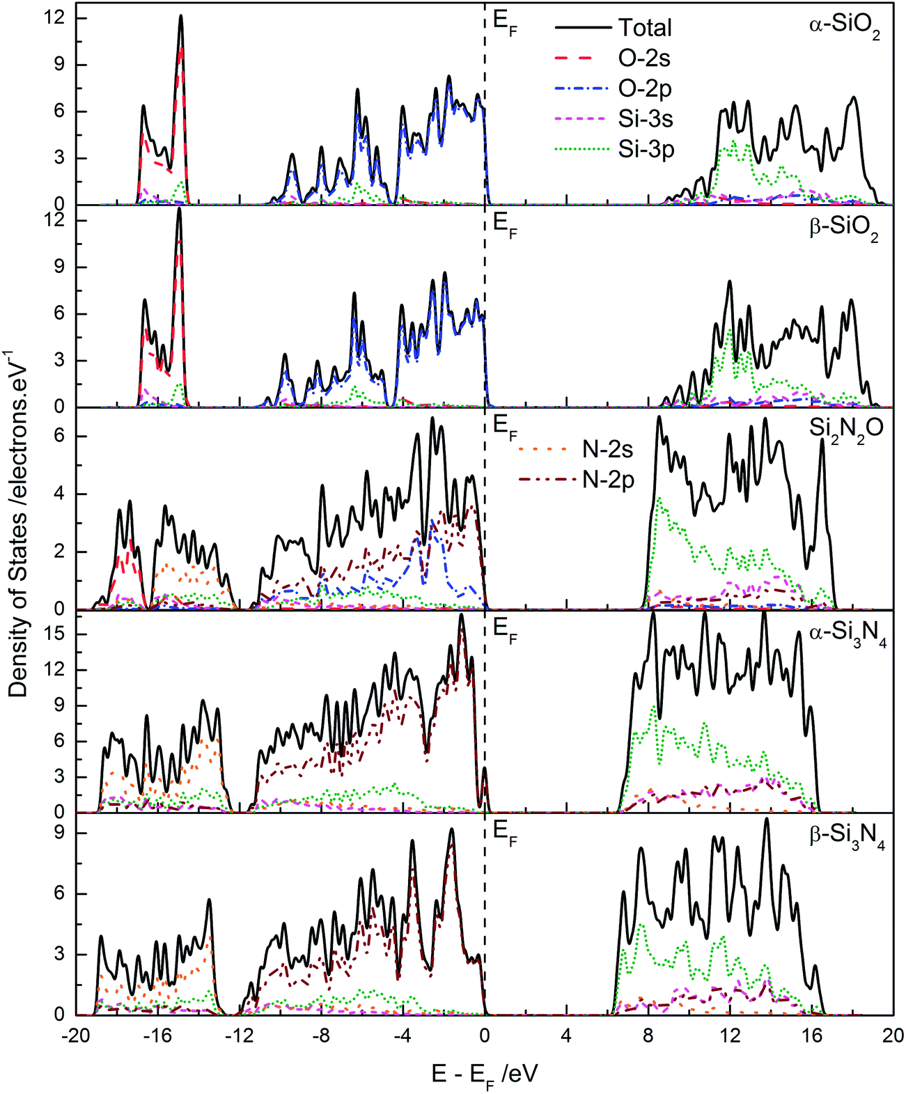 | ||
| Fig. 3 The calculated total and partial density of stature of Si–O–N compounds in different crystal structures. | ||
3.3 Optical properties
Fig. 4 illustrated the calculated dielectric function of five Si–O–N compounds. In the present work, the calculated values of the static dielectric constant ε0 of α-SiO2 is ∼1.67, which is very smaller than that of experimental measurement (∼4.5),33 but is similar with previously reported theoretical calculated results.27,29 The deviation between calculated results and experimental measurements maybe ascribe that only the straightforward electron transition from occupied states to unoccupied states is considered in DFT calculations. The calculated components of ε0 for all Si–O–N compounds are listed in Table 3. Firstly, the value of ε0 is increasing along with the increase of nitrogen content. Secondly, the ε0 of β-SiO2 is smaller than that of α-SiO2. The same phenomenon could be observed in Si3N4 compounds. As discussed above, the symmetry of β-SiO2 (or β-Si3N4) is higher than the symmetry of α-SiO2 (or α-Si3N4). Based on this calculated result, one could find that the optical properties not only are determined by the component of Si–O–N compounds, but also are determined by the microstructure of Si–O–N compounds. Thirdly, the intensity of dielectric function imaginary part is gradually becoming stronger along with the nitrogen content in the Si–O–N compounds. And the position of maximum of dielectric function (both real part and imaginary part) is gradually shifting toward lower-frequency range along with the nitrogen content in the Si–O–N compounds. | ||
| Fig. 4 The calculated dielectric functions of Si–O–N compounds in different crystal structures. | ||
The refractive index curves of these five Si–O–N compounds are plotted in Fig. 5. When the wavelength is smaller than 100 nm, the refractive index n is decreasing along with the N content; and then, the refractive index n is increasing along with the N impurity concentration. Finally, the refractive index n of α-SiO2 is converged to ∼1.292, and the refractive index n of other Si–O–N compounds is respectively converged to ∼1.273 (β-SiO2), ∼1.472 (Si2N2O), ∼1.629 (α-Si3N4), and ∼1.625 (β-Si3N4). There are two rules could be found: (i) the refractive index n is mainly determined by the proportion between oxygen and nitrogen in these five Si–O–N compounds, and is gradually increasing along with the nitrogen content; (ii) for the same Si–O–N compound, the refractive index n is slightly decreasing along with the increase of symmetry of crystal structure. For the refractive index k, namely extinction coefficient, the intensity is gradually increasing along with the increase of nitrogen content in these five Si–O–N compounds. At the same time, the band edge on the side of long wavelength is gradually red-shifting. The corresponding calculated reflectivity and absorption spectra of these five Si–O–N compounds are shown in Fig. 6. For these five Si–O–N compounds, the obvious light reflection is concentrated in range of 50–200 nm. When the wavelength is larger than 200 nm, the reflectivity of Si–O–N compounds is respectively converged toward a certain values: ∼0.016 (α-SiO2), ∼0.014 (β-SiO2), ∼0.036 (Si2N2O), ∼0.057 (α-Si3N4), and ∼0.056 (β-Si3N4). This calculated result indicates that the visible-light reflection is enhanced as increasing nitrogen content, which is very worthy of attention if one used Si–O–N compounds films as anti-reflective layer. The light absorption properties of Si–O–N compounds are very similar with that of the refractive index k, as shown in Fig. 5: the light absorption in the range of 50–200 nm is gradually enhancing along with the increase of nitrogen content, and the absorption edge is also gradually red-shifting along with the increase of nitrogen content, owing to the narrowing of band gap and the enhancing electron occupied probability on the bottom of CB.
 | ||
| Fig. 5 The calculated refractive index of Si–O–N compounds in different crystal structures. | ||
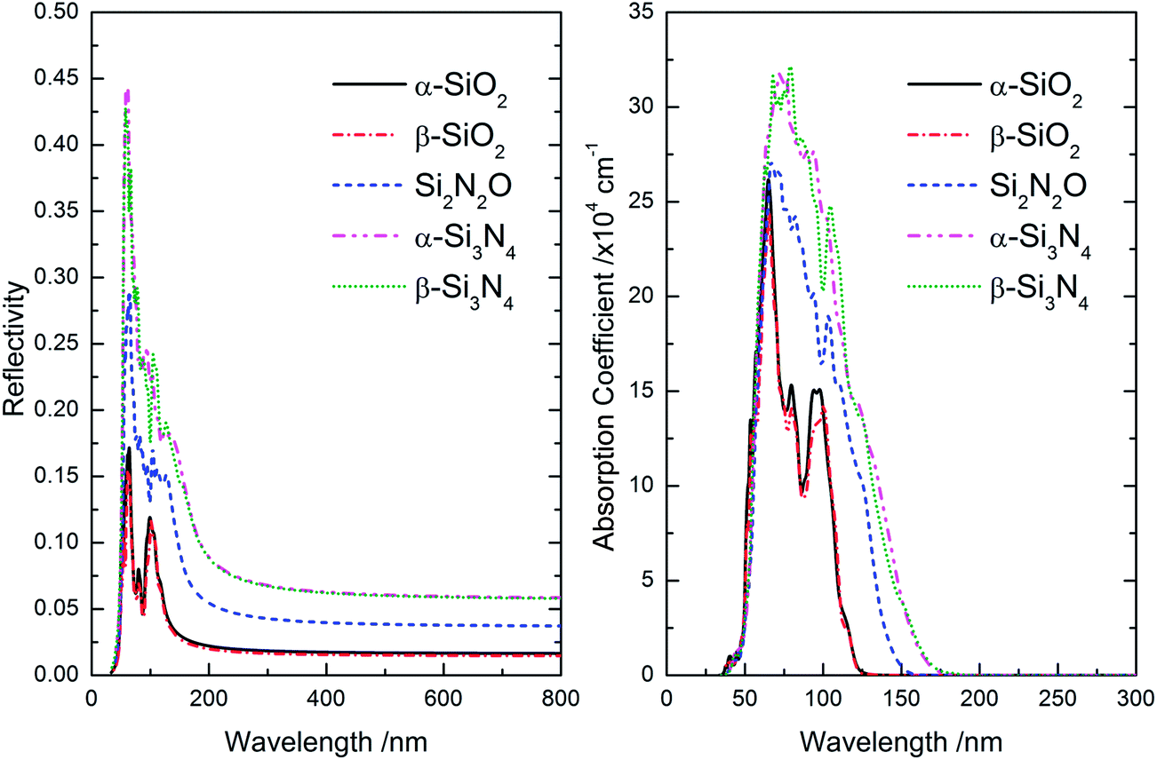 | ||
| Fig. 6 The calculated reflectivity and absorption spectra of Si–O–N compounds in different crystal structures. | ||
The optical properties of Si–O–N compounds are determined by their composition, crystal structure, and electronic structure. In turn, the differences of optical properties between these five Si–O–N compounds could reflect the subtle differences between their crystal structure and electronic structure. Firstly, the N-related energy levels have relatively higher position, compared with O-related energy levels. So, the VBM of Si–O–N compound could be shifted upward by increasing nitrogen content, resulting in band gap narrowing. And then, the optical properties are varied by the increase of nitrogen content, including: the dielectric function constant, refractive index, reflectivity, absorption edge, and so on. Secondly, the different crystal structure (including: symmetry, connection mode of tetrahedrons, coordination number, etc.) leads to different atomic interaction. Thus, there are distinct chemical bond and electron distribution between atoms in different Si–O–N compounds. In Table 1, the average Mulliken population of atoms and bonds is also listed. For all the atoms (except Si atoms) and bonds, the populations exhibit the same increasing tendency along with the increase of nitrogen content in these five Si–O–N compounds. These calculated results indicate that the ionic interaction of Si atoms with O or N atoms is gradually weakening, while the covalent interaction of Si atoms with O or N atoms is gradually enhancing, from SiO2 to Si2N2O to Si3N4. Just above intrinsic reasons to make the differences of optical properties of Si–O–N compounds. According to this principle, one could design novel Si–O–N compounds for specific optoelectronic applications, via controlling the composition and crystal structure.
4. Conclusions
The crystal structure, electronic structure, and optical properties of five Si–O–N compounds (including: α-quartz SiO2, β-quartz SiO2, Si2N2O, α-Si3N4, β-Si3N4) have been calculated by DFT within GGA+U method. From SiO2 to Si2N2O and to Si3N4, as the oxygen component is gradually replaced by nitrogen component, the band gap (include the minimum band gap and the direct band gap at Γ k-point) is also gradually narrowing, which is caused by upward shifting of valence band top that is composed by the O-2pπ and/or N-2pπ nonbonding states. The optical properties of Si–O–N compounds, including: the dielectric function constant, refractive index, reflectivity, absorption edge, and so on, are generally increasing along with the increase of nitrogen content. Furthermore, the microstructure of crystal in Si–O–N compounds also impact the detailed optical properties. In other words, the optical properties not only are determined by the component of Si–O–N compounds, but also are determined by the microstructure of Si–O–N compounds. These calculated results will be useful as reference data for analyzing the optical properties of more complicated SiOxNy compounds. According to this principle, one could design novel Si–O–N compounds for specific optoelectronic applications, via controlling the composition and crystal structure.Acknowledgements
The authors would like to acknowledge financial support from the National Natural Science Foundation of China (Grant no. U1037604).References
- O. W. Flörke, H. A. Graetsch, F. Brunk, L. Benda, S. Paschen, H. E. Bergna, W. O. Roberts, W. A. Welsh, C. Libanati, M. Ettlinger, D. Kerner, M. Maier, W. Meon, R. Schmoll, H. Gies and D. Schiffmann, in Ullmann's Encyclopedia of Industrial Chemistry, Wiley-VCH Verlag GmbH & Co. KGaA, 2000 Search PubMed.
- F. L. Riley, J. Am. Ceram. Soc., 2000, 83, 245 CrossRef CAS PubMed.
- M. E. Washburn, Am. Ceram. Soc. Bull., 1967, 46, 667 CAS.
- W. Qiu, Y. M. Kang and L. L. Goddard, Appl. Phys. Lett., 2010, 96, 141116 CrossRef PubMed.
- G. D. Wilk, R. M. Wallace and J. M. Anthony, J. Appl. Phys., 2001, 89, 5243 CrossRef CAS PubMed.
- P. Tung-Ming, L. Tan Fu and C. Tien Sheng, IEEE Electron Device Lett., 2000, 21, 378 CrossRef.
- M. L. Green, E. P. Gusev, R. Degraeve and E. L. Garfunkel, J. Appl. Phys., 2001, 90, 2057 CrossRef CAS PubMed.
- R. Germann, H. W. M. Salemink, R. Beyeler, G. L. Bona, F. Horst, I. Massarek and B. J. Offrein, J. Electrochem. Soc., 2000, 147, 2237 CrossRef CAS PubMed.
- G. L. Bona, R. Germann and B. J. Offrein, IBM J. Res. Dev., 2003, 47, 239 CrossRef CAS.
- J. Weber, H. Bartzsch and P. Frach, Appl. Opt., 2008, 47, C288 CrossRef CAS.
- H. Dong, K. Chen, D. Wang, W. Li, Z. Ma, J. Xu and X. Huang, physica status solidi (c), 2010, 7, 828 CAS.
- C. H. Chang, P. Yu and C. S. Yang, Appl. Phys. Lett., 2009, 94, 051114 CrossRef PubMed.
- C.-H. Sun, P. Jiang and B. Jiang, Appl. Phys. Lett., 2008, 92, 061112 CrossRef PubMed.
- D. Fischer, A. Curioni, S. Billeter and W. Andreoni, Phys. Rev. Lett., 2004, 92, 236405 CrossRef.
- Q. Weibin, M. Yuhui, Z. Jing, W. Jia-xian, L. Mengke, L. Shiyan and P. Jiaoqing, Jpn. J. Appl. Phys., 2014, 53, 021501 CrossRef.
- P. S. Peercy, Nature, 2000, 406, 1023 CrossRef CAS PubMed.
- C. McGuinness, D. Fu, J. E. Downes, K. E. Smith, G. Hughes and J. Roche, J. Appl. Phys., 2003, 94, 3919 CrossRef CAS PubMed.
- R. K. Pandey, L. S. Patil, J. P. Bange, D. R. Patil, A. M. Mahajan, D. S. Patil and D. K. Gautam, Opt. Mater., 2004, 25, 1 CrossRef CAS PubMed.
- F. Rebib, E. Tomasella, M. Dubois, J. Cellier, T. Sauvage and M. Jacquet, Thin Solid Films, 2007, 515, 3480 CrossRef CAS PubMed.
- F. Rebib, E. Tomasella, J. P. Gaston, C. Eypert, J. Cellier and M. Jacquet, J. Phys.: Conf. Ser., 2008, 100, 082033 CrossRef.
- S. J. Clark, M. D. Segall, C. J. Pickard, P. J. Hasnip, M. J. Probert, K. Refson and M. C. Payne, Z. Kristallogr., 2005, 220, 567 CAS.
- J. P. Perdew, A. Ruzsinszky, G. I. Csonka, O. A. Vydrov, G. E. Scuseria, L. A. Constantin, X. Zhou and K. Burke, Phys. Rev. Lett., 2008, 100, 136406 CrossRef.
- V. I. Anisimov, J. Zaanen and O. K. Andersen, Phys. Rev. B: Condens. Matter Mater. Phys., 1991, 44, 943 CrossRef CAS.
- B. G. Pfrommer, M. Câté, S. G. Louie and M. L. Cohen, J. Comput. Phys., 1997, 131, 233 CrossRef CAS.
- R. W. G. Wyckoff and R. Wyckoff, Crystal structures, Interscience publishers New York, 1963 Search PubMed.
- C. Brosset and I. Idrestedt, Nature, 1964, 201, 1211 CrossRef CAS.
- Y.-N. Xu and W. Y. Ching, Phys. Rev. B: Condens. Matter Mater. Phys., 1995, 51, 17379 CrossRef CAS.
- S. S. Nekrashevich and V. A. Gritsenko, Phys. Solid State, 2014, 56, 207 CrossRef CAS.
- Y.-N. Xu and W. Y. Ching, Phys. Rev. B: Condens. Matter Mater. Phys., 1991, 44, 11048 CrossRef CAS.
- P. Rulis, J. Chen, L. Ouyang, W.-Y. Ching, X. Su and S. Garofalini, Phys. Rev. B: Condens. Matter Mater. Phys., 2005, 71, 235317 CrossRef.
- Y.-C. Ding, M. Chen, X.-Y. Gao and M.-H. Jiang, Chin. Phys. B, 2012, 21, 067101 CrossRef.
- V. A. Gritsenko, J. B. Xu, R. W. M. Kwok, Y. H. Ng and I. H. Wilson, Phys. Rev. Lett., 1998, 81, 1054 CrossRef CAS.
- F. Gervais and B. Piriou, Phys. Rev. B: Solid State, 1975, 11, 3944 CrossRef CAS.
| This journal is © The Royal Society of Chemistry 2014 |