Preparation of hierarchically structured anodic aluminum oxide by a hexagonal embedded nanosphere array

Ming Cong, Yuyang Wang, Xinnan Wang, Yi Wang, Shuping Xu and Weiqing Xu*
State Key Laboratory of Supramolecular Structure and Materials, Institute of Theoretical Chemistry, Jilin University, 2699 Qianjin Ave, Changchun 130012, China. E-mail: xuwq@jlu.edu.cn; Fax: +86-431-85193421; Tel: +86-431-85159383

Received 18th June 2014 , Accepted 1st September 2014

First published on 3rd September 2014


Abstract

This study explored a built-in nanosphere template for anodic aluminum oxide (AAO) preparation and a hierarchically structured AAO with multilayered channels was achieved. A “defect anodization” mechanism based on a new voltage/interpore distance relationship was proposed and would be a reference for the AAO preparation based on pre-patterning methods.
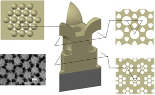

Anodic aluminum oxide (AAO) with relatively ordered channels is an important template and shadow mask to build large-area nanostructures.1 Compared with polymer templates, AAO has higher optical transmittance, better chemical/thermal stability and is an insulator. The preparation technology of AAO is simple, inexpensive, efficient and becomes mature based on reliable reproducibility. Normally, AAO pores are uniform and straight, and can self-organize to a nearly hexagonal close-packed arrangement. Interpore distance can be precisely regulated in a wide range of scale (50–420 nm)2 and the pore size can be tuned in a range of 5–400 nm.3–7 Each unit has the same morphology including consistent directionality and prominent aspect ratio, ensuring the materials filled in channels keep consistent properties. Therefore, AAO has a wide range of applications in solar cells,8 magnetic storage,9 high density of field emission, nano-capacitor and other fields.10,11

With the further requirements of AAO applications, more orderly periodic structures are in great demand. Since Masuda reported a two-step anodization method,4 the AAO pore distribution has been improved much orderly. He further developed a hard stamping method to pre-pattern ordered nanoindentations on Al surface.12 By this means, an AAO pore array with a large-scaled high order can be formed through anodic oxidation at a proper voltage as D = 2.5 V (D is interpore distance with the unit of nanometer and V is voltage with the unit of volt, put forward by Keller)1 and the defects of the array will be eliminated. In addition, many patterning approaches, such as focused ion beam,13 electron-beam lithography and nano-imprinting,14 have been used for constructing concaves on Al surfaces. In our previous work, we adopted nanosphere lithography (NSL)15 to pre-pattern Al substrates and eventually achieved a hierarchical honeycomb-like AAO after anodization at a special voltage one time lower than Keller empirical formula.16 The hierarchical structure as a template supports the wider application of AAO.17

Previous work noted that the template structure on Al surface could guide the AAO pore formation.16,17 If the pre-patterned template is embedded below Al surface, how would it have an impact on the growth of the AAO pores? To answer this question, in this work, we constructed a built-in template that a monolayer of polystyrene (PS) nanospheres was embedded in an Al substrate. Then, we anodized this special pre-patterned Al substrate at undervoltage condition and finally obtained an AAO with a new morphology and branch channels. The growth mechanism of this hierarchical AAO was discussed in this study.

Fig. 1 (left panel) shows the preparation process of a built-in template with PS nanospheres embedded in. First, on a pre-treated flat Al substrate (Fig. 1A), a monolayer of PS nanospheres were arranged through the gas/liquid interface self-assembly method (Fig. 1B).18 From the SEM image (Fig. 1F), it is obvious that the formed PS nanoshperes array is a hexagonal close-packed monolayer with the period of 550 nm, which equals the diameter of PS nanospheres. Then, the PS nanosphere monolayer experienced oxygen reactive ion etching (4.5 min) to reduce its size from 550 to 440 nm (Fig. 1G). We afterward deposited 500 nm Al on the shrunk PS nanosphere monolayer. Fig. 1H displays that Al covered the PS nanosphere monolayer completely and replicated the morphology of PS nanosphere monolayer with a little roughness. The cross section of the Al in which PS nanosphere monolayer was embedded is shown in Fig. 1J. The black arrow indicates a semi-exposed PS nanosphere and a white arrow points out a spherical hole formed after a PS nanosphere had been removed. These results show that PS nanospheres have been embedded under Al surface successfully, and the built-in template has been fabricated. The pre-patterned built-in Al template was used for anodization treatment. We optimized anodization voltage to 110 V and achieved a unique hierarchical pore structure as shown Fig. 1I. The morphology of the AAO became much rougher than that of the Al substrate. There are six pores formed around each bump. These pores grew larger via the chemical etching in phosphoric acid (5 wt%, 45 min and 30 °C), showing triangular profiles from the top view of Fig. 1K. At the same time, the tiny pores on the bumps became obvious, like a “cauliflower” array.


image file: c4ra05889e-f1.tif
Fig. 1 The flow chart of the preparation of AAO (left panel) and the SEM images at different stages (right panel). (A) An Al substrate. (B) A monolayer of self-assembled PS nanospheres on the Al substrate. (C) A monolayer of shrunk PS nanospheres by the treatment of the O2 reactive ion etching. (D) A pre-patterned built-in Al template that the PS nanospheres are embedded in Al via completely coating substrate C by the vacuum evaporation Al deposition. (E) The AAO substrate after anodization. (F), (G), (H) and (I) are the SEM images corresponding to (B), (C), (D) and (E), respectively. The PS nanospheres were 550 nm in diameter. The treatment of the O2 reactive ion etching was 4.5 min for achieving substrate C. The vacuum deposited Al was 500 nm in thickness and the anodization voltage for substrate D was 110 V. (J) Shows the cross-sectional view of substrate H. (K) is a pore-widened AAO substrate prepared by chemical etching substrate I in phosphoric acid (5 wt%) at 30 °C for 45 min. All SEM images are in the same magnification and the scale bar is 1 μm.

Fig. 2A displays the side view of the pore structure formed inside the AAO. It can be observed that the internal structure involves a monolayer of PS nanosphere array and two kinds of AAO channel structures, growing above or below the PS nanosphere array. It is obviously different from other AAOs that the pre-patterned periodic nanoindentations on Al substrates were used and the formation of pores started with nanoindentations during anodization. In present design, the built-in PS nanosphere array not only affects the channel arrangement in 2D plane, but also has impact on the longitudinal prolongation of channels. In order to discuss the channel growth process under the guide of the built-in PS nanosphere array, the whole channel growth is divided into three stages: (1) the formation of pores on the built-in Al substrate, (2) the branching of channels, when they pass through the PS nanosphere array and (3) the continuous growth of channels.


image file: c4ra05889e-f2.tif
Fig. 2 SEM images of AAO substrates prepared by a built-in PS nanosphere template with 500 nm thickness Al covering. Images A and B show the cross sections of AAO substrates obtained by the anodization time of 30 and 10 min, respectively. C and D respectively show the top and cross sections of AAO substrate A below PS nanospheres.

In the first stage, as shown in Fig. 2B, AAO channels began to grow vertically downward to the Al surface, forming straight holes. Channels always started to grow at the centre among every three bumps, forming a hexagonal channel array eventually in top view (Fig.3A). It is because electric field is more concentrated in these concaves. Thus, these concaves (in the centre of every three bumps) were more likely to induce the dissolution and the growth of oxide, forming a channel array on the surface of Al substrate. The observed interpore distance is ∼280 nm. At the same time, the anodization also happened on the Al above the PS nanospheres. A “cauliflower” array can be observed from either Fig. 2A or B.

In the second stage, the AAO channels continued growing on the built-in template. Since most space was occupied by PS nanospheres, channel only grew in the Al wall among PS nanospheres. With the increase of oxidation time, channels extended downward through the PS nanosphere layer. At the same time, the Al below PS nanospheres became oxidized and formed channels which connected to the cavities of PS nanospheres. During the anodization process, the produced oxygen needs an escaping way. It broke the barrier wall of PS nanospheres' cavities and connected the cavities with previous channels, forming a tri-branch geometry as shown in Fig. 3C and D. From the top view, the pore among nanospheres looks like a triangle if we widen the pores by chemical etching (Fig. 1K and 3E).


image file: c4ra05889e-f3.tif
Fig. 3 Schematic diagram of the AAO substrate obtained by anodizing a built-in PS nanosphere template. (A) Surface topography in top view. (B) Side view of a single cell. (C) The internal path of AAO channels. (D) The AAO structure of a single cell without PS nanospheres. (E) and (F) The cross section views along different depths.

In the third stage, the channels stably grew below the PS nanosphere monolayer. From Fig. 2C, we can observe that one unit below a PS nanosphere is composed of seven pores (Fig. 3F), which is a similar structure with the hierarchical AAO previously reported by our group.16 This geometry is only obtained by using the undervoltage anodization, that is, the anodization voltage of one time lower than Keller empirical formula was used. Based on the voltage/interpore distance empirical formula as D = 2.5 V, a certain voltage is adopted to achieve a designed period, which is an instinct and self-organized period of AAO. In many AAO preparation methods via pre-patterning,9,10,19–21 the selective voltage is also in accordance with the empirical formula and the achieved AAO channels strictly prolongated the prepatterns in depth. These AAO nanochannels fabricated by anodizing nanopatterned Al surface with empirically matched voltage can be termed as “perfect anodization”. However, to design a hierarchical periodic AAO, the pre-patterns give additional period on Al substrates, which differs from the self-organized period of AAO and requires a much lower anodization voltage relative to Keller's empirical formula. Owing to this “mismatched” voltage, more channels formed in individual PS nanosphere occupied indentation.22 Initially six pores grew prior in the edges of the indentation, as the reaction, the center of the indentation was etched, forming one pore. Therefore, we achieved seven pores below each PS nanosphere as shown in Fig. 3F (proved by Fig. 2C and D). In comparison, we term this process of preparing hierarchical AAO channels within one pre-patterned indentation as “defect anodization”.

At last, we obtained a multilayered composite AAO structure. There are two kinds of channels lying above and below PS nanosphere layer and they were connected through the PS nanospheres' cavities (Fig. 3D).

Conclusions

In summary, we prepared a composite AAO channel structure by anodizing a built-in PS nanosphere monolayer template. From top view, this composite AAO is composed of a hexagonal “cauliflower” array and a trigonal pore array (Fig. 3E). Interestingly, there is a hierarchical channel array below PS nanospheres with each PS nanosphere occupied indentation containing seven pores (Fig. 3F). Two pore layers are connected with the middle PS nanospheres' cavities and the cavities become a part of the channels. This study made an attempt on the utilization of the built-in template for AAO preparation. And we proposed a “defect anodization” mechanism against other “perfect anodization” examples based on a new voltage/interpore distance relation to explain the growth mechanism of hierarchical AAO channel structures. This mechanism will be a reference for the preparation of highly ordered AAO based on the pre-patterning methods.

Acknowledgements

This work was supported by the National Instrumentation Program (NIP) of the Ministry of Science and Technology of China no. 2011YQ03012408, National Natural Science Foundation of China (no. 21373096, 21073073, and 91027010) and Innovation Program of the State Laboratory of Supramolecular Structure and Materials, Jilin University.

Notes and references

  1. F. Keller, M. S. Hunter and D. L. Robinson, J. Electrochem. Soc., 1953, 100, 411 CrossRef CAS PubMed.
  2. P. Li, F. Müller, A. Birner, K. Nielsch and U. Gösele, J. Appl. Phys., 1998, 84, 6023 CrossRef PubMed.
  3. W. Lee, R. Ji, U. Gösele and K. Nielsch, Nat. Mater., 2006, 5, 741 CrossRef CAS PubMed.
  4. H. Masuda and K. Fukuda, Science, 1995, 268, 1466 CAS.
  5. H. Masuda, F. Hasegwa and S. Ono, J. Electrochem. Soc., 1997, 144, L127 CrossRef CAS PubMed.
  6. H. Masuda, K. Yada and A. Osaka, Jpn. J. Appl. Phys., Part 2, 1998, 37, L1340 CrossRef.
  7. S. Shingubara, K. Morimoto, H. Sakaue and T. Takahagi, Electrochem. Solid-State Lett., 2004, 7, E15 CrossRef CAS PubMed.
  8. R. Karmhag, T. Tesfamichael, E. Wäckelgård, G. A Niklasson and M. Nygren, Sol. Energy, 2000, 68, 329 CrossRef CAS.
  9. K. Nielsch, R. B. Wehrspohn, J. Barthel, J. Kirschner, U. Gösele, S. F. Fischer and H. Kronmüller, Appl. Phys. Lett., 2001, 79, 1360 CrossRef CAS PubMed.
  10. G. Che, B. B. Lakshmi, E. R. Fisher and C. R. Martin, Nature, 1998, 393, 346 CrossRef CAS PubMed.
  11. C. Hennesthal, J. Drexler and C. Steinem, ChemPhysChem, 2002, 3, 885 CrossRef CAS.
  12. H. Masuda, H. Yamada, M. Satoh, H. Asoh, M. Nakao and T. Tamamura, Appl. Phys. Lett., 1997, 71, 2770 CrossRef CAS PubMed.
  13. B. Chen, K. Lu and Z. Tian, Langmuir, 2011, 27, 800 CrossRef CAS PubMed.
  14. T. S. Kustandi, W. W. Loh, H. Gao and H. Y. Low, ACS Nano, 2010, 4, 2561 CrossRef CAS PubMed.
  15. A. L. Lipson, D. J. Comstock and M. C. Hersam, Small, 2009, 5, 2807 CrossRef CAS PubMed.
  16. X. Wang, S. Xu, M. Cong, H. Li, Y. Gu and W. Xu, Small, 2012, 8, 972 CrossRef CAS PubMed.
  17. X. Wang, Y. Wang, M. Cong, H. Li, Y. Gu, J. R. Lombardi, S. Xu and W. Xu, Small, 2013, 9, 1895 CrossRef CAS PubMed.
  18. J. C. Hulteen and R. P. Van Duyne, J. Vac. Sci. Technol., A, 1995, 13, 1553 Search PubMed.
  19. W. Lee, R. Ji, C. A. Ross, U. Gösele and K. Nielsch, Small, 2006, 2, 978 CrossRef CAS PubMed.
  20. A. S. M. Chong, L. K. Tan, J. Deng and H. Gao, Adv. Funct. Mater., 2007, 17, 1629 CrossRef CAS.
  21. Y. Matsui, K. Nishio and H. Masuda, Small, 2006, 2, 522 CrossRef CAS PubMed.
  22. S. Lee, D. Kim, E. Gillette, J. Oh, S. W. Hand and S. B. Lee, Phys. Chem. Chem. Phys., 2013, 15, 10659 RSC.

Footnote

Electronic supplementary information (ESI) available: (1) Materials and reagents, (2) instruments, (3) preparation of a built-in nanosphere template on Al sheets, (4) AAO obtained from a deep built-in template. See DOI: 10.1039/c4ra05889e

This journal is © The Royal Society of Chemistry 2014
Click here to see how this site uses Cookies. View our privacy policy here.