Liang Shi* and
Yanan Li
Department of Chemistry, University of Science and Technology of China, Hefei 230026, P. R. China. E-mail: sliang@ustc.edu.cn; Fax: +86-551-3607402; Tel: +86-551-3607234
First published on 9th September 2014
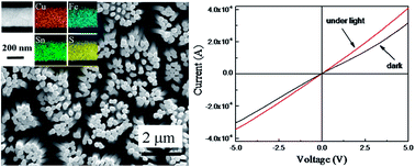
A single crystalline Cu2FeSnS4 nanowires array has been prepared via a convenient solution approach. Porous anodic aluminum oxide was used as a morphology directing template and played a significant role in the formation of single crystalline Cu2FeSnS4 nanowires. The as-prepared Cu2FeSnS4 nanowires are uniform with a [110] growth direction. Structure, morphology, composition and optical absorption properties of the as-prepared samples were characterized with X-ray powder diffraction, transmission electron microscopy, energy dispersive X-ray spectrometry, scanning electron microscopy and UV-Vis spectrophotometry. The formation mechanism of Cu2FeSnS4 nanowires array has been discussed. Thin films prepared from Cu2FeSnS4 single crystalline nanowires displayed an obvious photoelectric response, suggesting their potential application as low cost solar absorber materials.
The overall crystallinity of the product is examined by X-ray diffraction (XRD, Rigakau RU-300 with CuKα radiation). The general morphology of the products was characterized using scanning electron microscopy (FESEM QF400). Detailed microstructure analysis was carried out using transmission electron microscopy (TEM Tecnai 20ST). The chemical composition and the spatial distribution of the compositional elements in the product were examined using an energy dispersive X-ray (EDX) spectrometer and Gatan image filtering (GIF) system, attached to the same microscope. For the SEM measurements, several drops of 1 M NaOH aqueous solution were added onto the sample to dissolve some part of the AAO template. The residual solution on the surface of the template was rinsed with distilled water. For the TEM and HRTEM measurements, the template was completely dissolved in 2 M NaOH aqueous solution. The product was centrifuged, thoroughly washed with distilled water to remove residual NaOH and then rinsed with absolute ethanol. The UV-Vis spectrum of the product was recorded in a UV-Vis spectrophotometer (UV-1601PC, Shimadzu Corporation). I–V curves were measured by linear sweep voltammetry on CH Instrument 660C electrochemical analyzer. A photoresponse device structure was fabricated to study the optoelectronic properties of the as-synthesized nanowires. The fabrication details of the device structure are as follows: a insulating quartz substrate was used as the substrate and thoroughly washed with a mixed solution of deionized water, acetone, and 2-propanol under sonication for 30 min. RF sputtering of Au electrodes were then completed on insulating quartz substrates. The Cu2FeSnS4 film was fabricated by dripping the concentrated nanowires methanol dispersion on the electrodes and the substrate, and then drying it for 5 hours at room temperature under ambient conditions. A post-anneal process was conducted at 300 °C in an Ar atmosphere to improve substrate adhesion.
Fig. 2 shows a SEM image of the as-prepared sample with the AAO template partially removed. A highly ordered array of well-distributed nanowires are grown in a large area. These nanowires are continuous, smooth and parallelly aligned. The size distribution of the as prepared nanowires is uniform over the entire area and the average diameter of the nanowires is 200 nm ± 10 nm, which is consistent with the pore size dimension of the AAO template.
The microstructure and chemical composition of Cu2FeSnS4 nanowires have been studied with TEM studies accompanied by selected area electron diffraction (SAED) and energy dispersive X-ray spectrometry (EDX). A representative TEM image in Fig. 3a indicates that the as-prepared Cu2FeSnS4 nanowires are straight with smooth surface. These nanowires have an average diameter of 200 nm, this is consistent with the pore size dimension of the AAO template. The selected-area electron diffraction (SAED) pattern of the nanowires is displayed in the inset of Fig. 3a, which shows clear symmetrical diffraction spots, disclosing the single crystalline nature of the Cu2FeSnS4 nanowires. A high resolution TEM (HRTEM) image shown in Fig. 3b reveals clear lattice spacing of 0.385 nm which is calculated from the line profile in Fig. 3c. This value of 0.385 nm corresponds well to the d spacing of the (110) planes in tetragonal stannite structured Cu2FeSnS4, confirming the well-crystallized nanowires. The inset of Fig. 3b shows a two-dimensional Fourier transform pattern of the lattice resolved image, which can be indexed to the [11] zone of tetragonal stannite Cu2FeSnS4, demonstrating the [110] growth direction and single crystallinity of the Cu2FeSnS4 nanowires. The EDX spectrum (Fig. 3d) taken from the sample reveals intense peaks of Cu, Fe, Sn and S, indicating the chemical composition of Cu, Fe, Sn and S, only. The gold and carbon signals come from the supporting TEM grid. EDX quantitative analysis gives an average Cu/Fe/Sn/S composition (%) of 25.18 13.12
:
13.27
:
48.43, being close to molar ratio of 2
:
1
:
1
:
4 and in accordance with the stoichiometry of Cu2FeSnS4.
STEM-EDX elemental mapping can provide information on the spatial distribution of different compositional elements in the Cu2FeSnS4 nanowires. Fig. 4 shows the dark field image of a portion of the Cu2FeSnS4 single nanowire and gives the elemental maps of Cu, Fe, Sn and S, respectively. The uniform spatial distribution of different compositional elements in Cu2FeSnS4 nanowires is illustrated evidently in the elemental maps.
![]() | ||
Fig. 4 Dark field image of a portion of a Cu2FeSnS4 nanowire and EDX elemental maps of Cu, Fe, Sn S, respectively. |
Dark black color of the as-prepared Cu2FeSnS4 nanowires is observed, suggesting its strong photon absorption in the entire visible range of light. Fig. 5 shows the room temperature UV-Vis absorption spectrum for the as-prepared Cu2FeSnS4 nanowires sample, indicating broad and strong optical absorption in the UV-visible region. Estimation on the optical band gap (Eg) of the Cu2FeSnS4 nanowires can be obtained by plotting (αhν)2 as a function of the photon energy (in the inset of Fig. 5), with α being the absorption coefficient, h Planck's constant, and ν the frequency. The Eg value is calculated to be 1.42 eV based on the intersection of the extrapolated linear portion, being consistent with that of reported value (1.28–1.54 eV) for Cu2FeSnS4.1,2 Such band gap value is desirable for the potential photovoltaic applications.
It has been found that the porous AAO template plays a decisive role in the synthesis of single-crystalline Cu2FeSnS4 nanowires. If AAO template was not used with other reaction conditions unchanged, Cu2FeSnS4 nanoparticles, instead of nanowires array, can be obtained. Fig. 6a shows a typical XRD pattern of Cu2FeSnS4 nanoparticles. All diffraction peaks can be indexed to the stannite structured Cu2FeSnS4. The obviously broadening of XRD peaks suggests that the as-prepared Cu2FeSnS4 particles are of very small sizes. Based on the Scherrer equation, D = (0.89λ)/β(cosθ), here λ is the wavelength for the Kα1 (1.54056 Å), β is the peak width at half-maximum in radians and θ is the Bragg's angle, the average particle size was calculated to be 35 nm. The particle size result is consistent with later TEM analysis. A TEM image in Fig. 6b indicates that the as-prepared product is composed of a lot of aggregated nanoparticles with size in the range of 20–50 nm. The diffraction rings of the selected-area electron diffraction (SAED) pattern taken from these nanoparticles, as displayed in the inset of Fig. 6b, reveal polycrystalline nature of Cu2FeSnS4 sample and can be indexed to (112), (220) and (312) reflections, consistent with the expected tetragonal crystal lattice. The EDX spectrum (Fig. 6c) taken from the sample reveals intense peaks of Cu, Fe, Sn and S, displaying the chemical composition of Cu, Fe, Sn and S, only. EDX quantitative analysis gives an average Cu/Fe/Sn/S molar ratio of nearly 2
:
1
:
1
:
4, in accordance with the stoichiometry of Cu2FeSnS4.
The observation from above controlled experiment suggests that random polycrystalline nanoparticles should formed during the initial stage of reaction process. In the case with the use of AAO template, many random nanocrystals should be produced confined within the pores of AAO template, and then, a subsequent crystal growth process continued. It is known that nanocrystals have high surface energy and they tend to contact and grow together or fuse into larger particles to decrease the surface energy. Oriented attachment mechanism can be used to explain the crystal growth in which smaller particles with common crystallographic orientations directly combine together to form larger ones by crystallographic fusion at the planar interface. During the process of oriented attachment, random particles with no common crystallographic orientation tend to rotate into an orientation to obtain the structural accord at the interface. Then, a coherent grain–grain boundary is formed and disappeared when a single larger nanocrystal is produced finally. Since our present crystal growth occurs in long confined AAO pores, oriented attachment serves a most possible mechanism due to its not involving of diffusion of the grain boundary over large distance scales. In the long time reaction process, misoriented Cu2FeSnS4 grains rotate or reorient to obtain a structural accord at the interface and induced further crystal growth along the preferred growth axis [110] direction. As a result of the confinement of the AAO pores, one-dimensional single crystalline Cu2FeSnS4 nanowires with diameter determined by the pore size in the AAO template were generated, which is evidenced by the SEM and TEM characterization of our product.
To investigate the photoelectric properties, the current–voltage (I–V) measurements for the Cu2FeSnS4 nanowires thin films were performed. Fig. 7 shows the I–V curves of the films tested in the darkness and under an illumination intensity of 100 mW cm−2 from a 150 W Xenon lamp (Bentham IL7), which was measured in a 5 V bias range. It is found that an increase of about 29% in photocurrent at 5 V by under light irradiation relative to the dark state. In the present case, the energy from Xe light irradiation excites electrons in the Cu2FeSnS4 semiconductor from valance band to the conduction band and then increases the holes in the film. As a result, the current is increased obviously. This obvious photoelectric response suggests that the as-synthesized Cu2FeSnS4 nanowires would be a potential candidate in the fabrication of photovoltaic devices.
![]() | ||
Fig. 7 The current–potential (I–V) curve of the Cu2FeSnS4 film tested in the darkness (black line) and under illumination (red line). |
This journal is © The Royal Society of Chemistry 2014 |