
A morphology effect of hematite photoanode for photoelectrochemical water oxidation
Zilong Liu,
Kexin Wang,
Li Xiao*,
Xuejiao Chen,
Xiaodi Ren,
Juntao Lu and
Lin Zhuang*
College of Chemistry and Molecular Sciences, Hubei Key Lab of Electrochemical Power Sources, Wuhan University, Wuhan 430072, China. E-mail: chem.lily@whu.edu.cn; lzhuang@whu.edu.cn
First published on 5th August 2014
Abstract
Hematite has been a popular photoanode for photoelectrochemical water splitting; however, its performance varies widely in the literature. In-depth understanding of the structure–performance relationship of hematite photoanode is still lacking. Here, we report a finding that without the use of co-catalysts or any alteration in crystal structure, the performance of hematite photoanode can be markedly improved by properly enlarging the space among α-Fe2O3 nanocrystalline, i.e., by increasing the pore size in the electrode. Such a finding indicates that in addition to the known catalytic and crystal effects, the internal structure of the hematite electrode is also a very sensitive factor to PEC efficiency.
Because of the global oil crisis, a worldwide quest for alternative energy sources has been stimulated. Among the energy sources exploited, solar energy is tremendous and the most widely available.1 Thus, the harvesting of solar energy has intrigued a significant interest in both scientific and industrial communities.2 The photoelectrochemical (PEC) water splitting has been considered to be a practical way to store solar energy since Fujishima and Honda's pioneering work in 1970s.3 In a PEC conversion process, a semiconductor electrode absorbs the solar light and generates a separated electron–hole pair, which is used to split water. In the case of photoanode, the photo-induced holes migrate to the semiconductor–liquid interface and oxidize water, generating oxygen, while the photo-induced electrons go to the cathode through the external circuit.4 Among photoanode materials, hematite (α-Fe2O3) has received considerable attention because of its abundance, stability, environmental compatibility, and suitable band gap (ca. 2.2 eV).5,6 Although promising, hematite possesses obvious drawbacks, including short diffusion length of holes (<5 nm),7,8 sluggish catalytic dynamics,9 and high charge recombination rate.10 Because of these disadvantages, only the holes close to the semiconductor–liquid junction can contribute to the oxidization of water. Considering the light penetration length in α-Fe2O3 is of the order of 100 nm,5,11 most photo-induced holes in the bulk will recombine with the photo-induced electrons before they can reach the surface.
Stacking thin films of α-Fe2O3 was considered to be an effective way to minimize the hole transport distance;12 however, the surface area of this type of photoanode is not high enough. Resolution of this problem is to construct nanostructured electrodes making use of nanowire,13 nanotube,14 nanorod,15 among others. Among the reported nanostructured α-Fe2O3 photoanodes, the perpendicularly oriented tree-like structure, reported by Grätzel's group, showed the highest PEC efficiency.5 In this electrode structure, each α-Fe2O3 nanotree grows preferentially in [110] direction, which is considered to be favorable for hole transport.5,16 While several studies have focused on the growth mechanism and the morphology control of such a nanostructured photoanode,5,17,18 the in-depth understanding of the structure–property relationship is still lacking.
In this communication, we report a finding that in addition to the oriented growth of α-Fe2O3 nanotrees, the pore size in the electrode (i.e., the empty space among nanotrees) is also an important structural factor for improving PEC efficiency. The pore size in the hematite photoanode was deliberately controlled by introducing a thin, patterned Au sublayer, onto which the α-Fe2O3 layer was deposited. The Au sublayer was implemented in two fashions: nanoporous gold (NPG) film and gold island. The former was produced by sputtering a Au0.2Ag0.8 alloy film (ca. 100 nm in thickness) onto the fluorine-doped tin oxide (FTO) substrate, followed by leaching the Ag component in concentrated nitric acid for about 1 hour. The resulting NPG film consists of discrete Au flakes (Fig. 1a). The preparation of gold islands (GIs) includes two steps: sputtering a thin gold film (ca. 10 nm in thickness) on FTO, and then annealing at 500 °C for 30 minutes during which the thin gold film breaks and aggregates into gold islands (Fig. 1b).
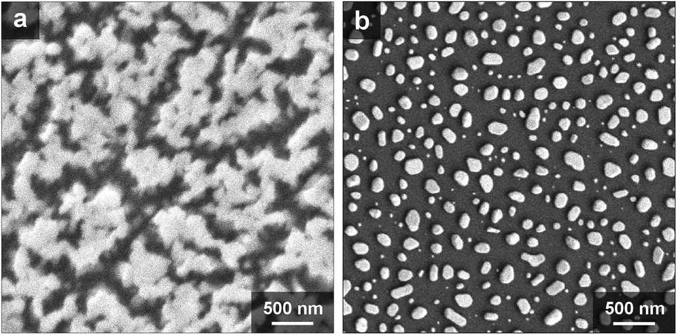 | ||
| Fig. 1 SEM images of the nanoporous gold (NPG) sublayer (a) and the gold islands (GIs) sublayer (b) on FTO substrate. | ||
The α-Fe2O3 layer was prepared by atmospheric pressure chemical vapour deposition (APCVD) on the basis of the thermal decomposition of iron pentacarbonyl in a homemade chamber, according to the design of Grätzel's group.17 Tetraethyl orthosilicate (TEOS) was used as the precursor of Si dopant. Argon was bubbled through the vials of iron and silicon precursors (23.2 ml min−1 for Fe(CO)5 and 13.5 ml min−1 for TEOS), and then mixed with oxygen before entering the CVD chamber. Fe(CO)5 and TEOS were decomposed on the hot FTO substrate (with or without Au sublayer), whose temperature was controlled to be 500 °C. Fig. 2 displays the SEM and AFM images of the hematite electrodes deposited on bare FTO and Au modified substrates. From the top views (Fig. 2a–c & g–i), these hematite electrodes appear to consist of particles with that on NPG/FTO having the biggest particle size; however, from section views (Fig. 2d–f), each particle is actually a α-Fe2O3 nanotree grown perpendicularly to the substrate surface. Whereas the α-Fe2O3 nanotrees grown on bare FTO are very dense (Fig. 2a, d & g), those on NPG/FTO are well separated (Fig. 2b, e & h). In other words, the pore size in the α-Fe2O3 layer on NPG/FTO increases significantly. The morphology of α-Fe2O3 on GIs/FTO (Fig. 2c, f & i), however, appears to be a combination of the above two cases. This could be because gold islands are sparsely distributed on FTO (Fig. 1b) and α-Fe2O3 can grow either on the gold island or on the exposed FTO substrate. Nevertheless, it is clear that the introduction of a thin, patterned Au sublayer changes the deposition pattern of the hematite layer, leading to an increase in the crystal size of α-Fe2O3 and the pore size of the electrode (which implies a decrease in the surface area of α-Fe2O3).
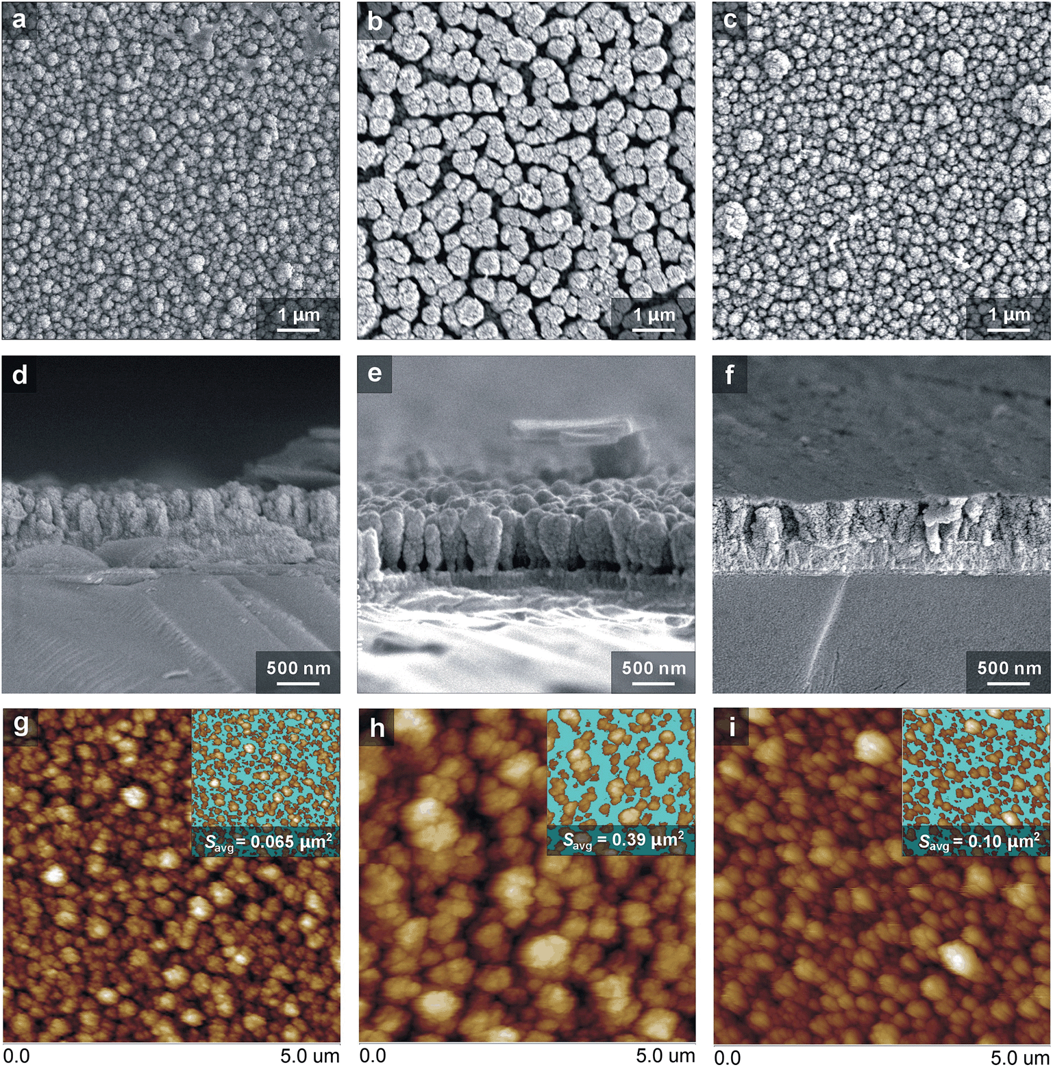 | ||
| Fig. 2 Top-viewed (a–c) and section-viewed (d–f) SEM images and AFM images (g–i) of the hematite electrode grown on bare FTO (a, d and g), NPG/FTO (b, e and h), and GIs/FTO (c, f and i). Insets in AFM images are the half-height slices for quantitative pore-size analysis. The averaged pore size (Savg) is extracted based on a particle-size recognition on the empty part of the slice (colored in sky blue). | ||
To quantitatively evaluate the pore size of the studied electrodes, the AFM images were sliced at a given altitude. The empty pattern in an AFM slice (the sky blue part in the insets of Fig. 2g–i) was subjected to particle size analysis using the NanoScope Analysis software, and the averaged pore size can thus be extracted. The insets in Fig. 2g–i are the half-height slice of the corresponding AFM image of the electrode. The averaged pore size was 0.065 μm2, 0.39 μm2, and 0.10 μm2 for the hematite electrode grown on bare FTO (Fig. 2g), on NPG/FTO (Fig. 2h), and on GIs/FTO (Fig. 2i), respectively. Note that the total area of the blue part turns out to be almost constant (ca. 10 μm2) in all these AFM slices (5 μm × 5 μm), indicating that the total empty volume (or the porosity) is almost the same in the three electrodes but the pore size is clearly different.
The PEC performance was tested in 1 M KOH solution using a three-electrode cell with Hg/HgO reference electrode (0 VHg/HgO = 0.926 VRHE) and platinum-wire counter electrode. The scan rate of linear sweeping voltammetry was 20 mV s−1 and the electrolyte was deaerated with argon during the experiment. An Oriel 300W xenon lamp (Newport, model 69911) served as the light source with an AM 1.5 G filter. As demonstrated in Fig. 3a, the consequence of increasing the pore size in hematite photoanode is remarkable. Whereas the photocurrent density on α-Fe2O3/FTO is only 0.15 mA cm−2 at 1.23 VRHE under illumination, those on α-Fe2O3/NPG and α-Fe2O3/GIs have been boosted to 0.45 and 0.71 mA cm−2, respectively. The photocurrent plateau, which is reported in most studies to be around 1.43 VRHE, is 0.74 mA cm−2 for α-Fe2O3/FTO and increases to 1.13 and 1.43 mA cm−2 for α-Fe2O3/NPG and α-Fe2O3/GIs, respectively. When the amount of α-Fe2O3 was controlled to be the same for the three electrodes, such an enhancement in photocurrent can only be attributed to the structural change in the photoanode. One may argue that the Au sublayers could also contribute to the PEC performance through certain surface plasmon resonance (SPR) effect;19 however, this factor should be rather minor, if not absolutely null, because the α-Fe2O3 layer is significantly thicker than the Au sublayer. In addition, on the basis of UV-vis spectroscopic results (Fig. 3b), the contribution of light harvesting of Au sublayers is negligible.
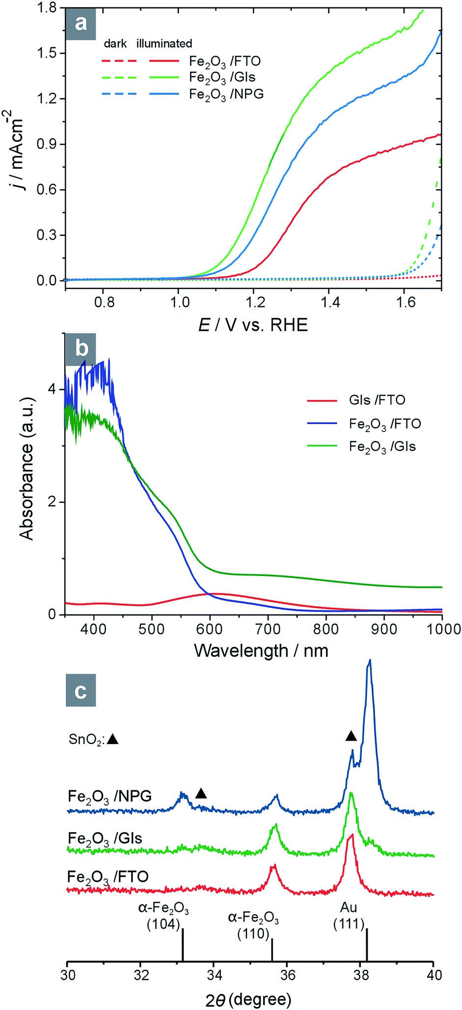 | ||
| Fig. 3 PEC performance (a), UV-vis spectra (b), and X-ray diffraction (XRD) patterns (c) of the studied electrodes and substrates. (Note: Samples with NPG sublayer are not transparent enough for transmission UV-vis observation). | ||
According to the X-ray diffraction (XRD) patterns (Fig. 3c), the α-Fe2O3 nanotrees grew, as expected, preferentially in [110] direction on either bare FTO or GIs/FTO, while on NPG/FTO, the (104) diffraction peak of α-Fe2O3 can also be observed. It appears that the NPG film, covering most of the FTO surface, has changed the growth mode of α-Fe2O3 during the APCVD process, while on GIs/FTO the FTO substrate is still well exposed; hence, the growth of α-Fe2O3 remained unchanged. This implies that the structural modification effect of GIs/FTO is purely to increase pore size in the hematite photoanode, while the NPG/FTO also alters the preferential orientation of hematite, which is a negative effect on the PEC performance.
The bigger crystal size of α-Fe2O3 on NPG/FTO or on GIs/FTO, in comparison to that on bare FTO, is also a negative effect on both electrocatalysis and charge transport because the specific surface area of hematite is reduced and the hole-transport distance in hematite crystalline increased. Therefore, the observed enhancement in PEC performance can only be attributed to the increase in the pore size in the electrode. The underlying mechanism is most probably related to the mass transport in the electrode. As shown in Fig. 4, the mass transport in the α-Fe2O3/FTO electrode with small pore size should be less efficient than that in the α-Fe2O3/NPG electrode with large pore size. However, the most efficient mass transport requires an optimized combination of large and small channels (Fig. 4c), a situation similar to the blood circulation system in our bodies and the structure of the α-Fe2O3/GIs electrode appears to fulfill this pattern.
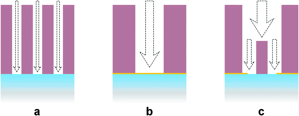 | ||
| Fig. 4 Schematic illustrations of the mass transport in α-Fe2O3/FTO (a), α-Fe2O3/NPG (b), and α-Fe2O3/GIs (c) electrodes. Among these patterns, pore volumes are almost the same but the pore sizes are different. | ||
The finding reported in this work provides valuable information for the design of photoanode for PEC water splitting. In addition to the factor directly related to the hematite nanocrystalline, such as preferential orientation and catalytic surface, pore size of the hematite electrode turns out to be an important parameter strongly influencing the PEC efficiency.
Acknowledgements
This work was financially supported by the National Basic Research Program (2012CB932800, 2012CB215500), the National Natural Science Foundation of China (21125312, 21203142), the Doctoral Fund of Ministry of Education of China (20110141130002), and the Fundamental Research Funds for the Central Universities.References
- (a) M. Grätzel, Nature, 2001, 414, 338 CrossRef PubMed; (b) T. W. Hamann, R. A. Jensen, A. B. F. Martinson, H. Van Ryswyk and J. T. Hupp, Energy Environ. Sci., 2008, 1, 66 RSC; (c) M. G. Walter, E. L. Warren, J. R. McKone, S. W. Boettcher, Q. Mi, E. A. Santori and N. S. Lewis, Chem. Rev., 2010, 110, 6446 CrossRef CAS PubMed; (d) Y. Qu and X. Duan, Chem. Soc. Rev., 2013, 42, 2568 RSC.
- (a) C. J. Brabec, N. S. Sariciftci and J. C. Hummelen, Adv. Funct. Mater., 2001, 11, 15 CrossRef CAS; (b) S. U. M. Khan, M. Al-Shahry and W. B. Ingler Jr, Science, 2002, 297, 2243 Search PubMed; (c) G. Li, V. Shrotriya, J. Huang, Y. Yao, T. Moriarty, K. Emery and Y. Yang, Nat. Mater., 2005, 4, 864 CrossRef CAS; (d) X. Chen, S. Shen, L. Guo and S. Mao, Chem. Rev., 2010, 110, 6503 CrossRef CAS PubMed; (e) Y. Hou, F. Zuo, A. Dagg and P. Feng, Nano Lett., 2012, 12, 6464 CrossRef CAS PubMed.
- A. Fujishima and K. Honda, Nature, 1972, 238, 37 CrossRef CAS.
- K. Sivula, F. Le Formal and M. Grätzel, ChemSusChem, 2011, 4, 432 CrossRef CAS PubMed.
- A. Kay, I. Cesar and M. Grätzel, J. Am. Chem. Soc., 2006, 128, 15714 CrossRef CAS PubMed.
- S. D. Tilley, M. Cornuz, K. Sivula and M. Grätzel, Angew. Chem., Int. Ed., 2010, 49, 6405 CrossRef CAS PubMed.
- A. Watanabe and H. Kozuka, J. Phys. Chem. B, 2003, 107, 12713 CrossRef CAS.
- Y. Lin, G. Yuan, S. Sheehan, S. Zhou and D. Wang, Energy Environ. Sci., 2011, 4, 4862 Search PubMed.
- M. P. Dare-Edwards, J. B. Goodenough, A. Hamnett and P. R. Trevellick, J. Chem. Soc., Faraday Trans. 1, 1983, 79, 2027 RSC.
- (a) N. J. Cherepy, D. B. Liston, J. A. Lovejoy, H. Deng and J. Z. Zhang, J. Phys. Chem. B, 1998, 102, 770 CrossRef CAS; (b) B. D. Chernomordik, H. B. Russell, U. Cvelbar, J. B. Jasinski, V. Kumar, T. Deutsch and M. K. Sunkara, Nanotechnology, 2012, 23, 194009 CrossRef PubMed.
- R. F. G. Gardner, F. Sweett and D. W. Tanner, J. Phys. Chem. Solids, 1963, 24, 1183 CrossRef CAS.
- (a) K. Itoh and J. O. Bockris, J. Appl. Phys., 1984, 56, 874 CrossRef CAS PubMed; (b) C. Jorand Sartoretti, M. Ulmann, B. D. Alexander, J. Augustynski and A. Weidenkaff, Chem. Phys. Lett., 2003, 376, 194 CrossRef CAS.
- (a) Y. Ling, G. Wang, D. A. Wheeler, J. Z. Zhang and Y. Li, Nano Lett., 2011, 11, 2119 CrossRef CAS PubMed; (b) M. T. Mayer, C. Du and D. Wang, J. Am. Chem. Soc., 2012, 134, 12406 CrossRef CAS PubMed.
- (a) S. K. Mohapatra, S. E. John, S. Banerjee and M. Misra, Chem. Mater., 2009, 21, 3048 CrossRef CAS; (b) Y. Lin, S. Zhou, S. W. Sheehan and D. Wang, J. Am. Chem. Soc., 2011, 133, 2398 CrossRef CAS PubMed.
- (a) A. Mao, N. Park, G. Y. Han and J. H. Park, Nanotechnology, 2011, 22, 175703 CrossRef PubMed; (b) S. Shen, C. X. Kronawitter, D. A. Wheeler, P. Guo, S. A. Lindley, J. Jiang, J. Z. Zhang, L. Guo and S. S. Mao, J. Mater. Chem. A, 2013, 1, 14498 RSC.
- (a) K. M. Rosso, D. M. A. Smith and M. Dupuis, J. Chem. Phys., 2003, 118, 6455 CrossRef CAS PubMed; (b) N. Iordanova, M. Dupuis and K. M. Rosso, J. Chem. Phys., 2005, 122, 144305 CrossRef CAS PubMed.
- (a) I. Cesar, K. Sivula, A. Kay, R. Zboril and M. Grätzel, J. Phys. Chem. C, 2009, 113, 772 CrossRef CAS; (b) M. Cornuz, M. Grätzel and K. Sivula, Chem. Vap. Deposition, 2010, 16, 291 CrossRef CAS PubMed.
- P. Zhang, A. K. Shwarsctein, Y. S. Hu, J. Lefton, S. Sharma, A. J. Forman and E. McFarland, Energy Environ. Sci., 2011, 4, 1020 CAS.
- (a) H. Gao, C. Liu, H. E. Jeong and P. Yang, ACS Nano, 2012, 6, 234 CrossRef CAS PubMed; (b) E. Thimsen, F. Le Formal, M. Grätzel and S. C. Warren, Nano Lett., 2011, 11, 35 CrossRef CAS PubMed; (c) J. Li, S. K. Cushing, P. Zheng, F. Meng, D. Chu and N. Wu, Nat. Commun., 2013, 4, 2651 Search PubMed.
| This journal is © The Royal Society of Chemistry 2014 |