Influence of the grain orientation on the charge transport properties of organic field-effect transistors

J. C. Ribierre*ab, Y. Yokotabc, M. Satoc, A. Ishizukabc, T. Tanakad, S. Watanabebe, M. Matsumotoe, A. Muranakab, S. Matsumoto*bc, M. Uchiyamabf and T. Aoyama*b
aDepartment of Physics, CNRS-Ewha International Research Center, Ewha Womans University, Seoul 120-750, South Korea
bElements Chemistry Laboratory, RIKEN, 2-1 Hirosawa, Wako, Saitama 351-0198, Japan. E-mail: ribierre@opera.kyushu-u.ac.jp; taoyama@riken.jp; smatsu@ynu.ac.jp
cDepartment of Environmental and Natural Sciences, Graduate School of Environment and Information Sciences, Yokohama National University, 79-2 Tokiwadai, Hodogaya-ku, Yokohama, Kanagawa 240-8501, Japan
dDepartment of Chemistry and Biochemistry, Fukushima National College of Technology, 30 Aza-Nagao, Tairakamiarakawa, Iwaki, Fukushima 970-8034, Japan
eDepartment of Materials Science and Technology, Tokyo University of Science, 6-3-1 Niijuku, Katsushika-ku, Tokyo 125-8585, Japan
fGraduate School of Pharmaceutical Sciences, The University of Tokyo, 7-3-1 Hongo, Bunkyo-ku, Tokyo 113-0033, Japan

Received 26th May 2014 , Accepted 30th July 2014

First published on 30th July 2014


Abstract

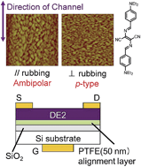
We report the effects of crystalline grain orientation on the charge transport properties of a J-aggregate bisazomethine dye (DE2) in thin films. Highly oriented DE2 organic field-effect transistors are fabricated using an insulating alignment layer of poly(tetrafluoroethylene) in the gate dielectric. An enhancement of about one and two orders of magnitude in hole mobility is achieved when the molecules and the crystalline grains are aligned perpendicular and parallel to the transistor channel, respectively. Ambipolar transport is observed only for the parallel alignment. To gain additional insights into the role of molecular packing on the charge transport properties of DE2, quantum chemical calculations are carried out to determine and compare the energetic splittings of the highest occupied molecular orbitals (HOMO) and of the lowest unoccupied molecular orbitals (LUMO) in the film. The results provide evidence that DE2 is intrinsically an ambipolar organic semiconductor and demonstrates the important role played by grain boundary orientation on charge trapping processes. Overall, the demonstration of field-effect mobilities as high as 0.01 cm2 V−1 s−1 and the observation of ambipolar transport in our devices represent an obvious milestone for the possible use of J-aggregate thin films in organic electronic devices. In addition, this work provides significant insights into the interplay between crystalline grain orientation and ambipolar charge transport properties in organic thin films.


Introduction

The charge transport properties of organic π-conjugated materials have been the subject of intensive studies during the last decades and have played an essential role in the performance of a variety of plastic optoelectronic devices.1 It is well established now that these properties are largely influenced by electron orbital overlap and spacing between adjacent conjugated molecules.1,2 Different approaches have been developed to control the molecular packing and improve the charge carrier mobilities of organic thin films.3–6 For example, Giri et al. recently reported a solution-processing technique for organic materials, in which lattice strain was used to decrease the π–π stacking distance and enhance the charge carrier mobilities.7 In the case of polycrystalline organic thin films, grain boundary effects on charge transport and charge trapping processes can be particularly detrimental to the performance of optoelectronic devices.8 Thus, controlling the molecular packing and the orientation of grain boundaries is essential for the enhancement of charge transport properties.9–11 It has also been demonstrated that changes in molecular packing can lead not only to an improvement of the charge carrier mobilities but also to a majority carrier type conversion.2,12–16 In this work, we demonstrate a significant enhancement of the ambipolar charge transport properties in highly oriented organic thin films by controlling the orientation of the molecules and the crystalline grains.

Molecular organization in the vapor-deposited J-aggregate organic thin films of N,N′-bis[4-(N,N-diethylamino)benzylidene]diaminomaleonitrile (DE2), as well as their third-order non-linear optical and photophysical properties was previously investigated in detail.17–22 The chemical structure of this neutral dye23 is shown in the inset of Fig. 1a. The good stability of the J-aggregates in DE2 films against heat and moisture was attributed to the non-ionic character of this molecule. Schottky-type organic photovoltaic cells based on J-aggregate DE2 thin films were fabricated and exhibited power conversion efficiencies in the visible region comparable with those typically obtained in metal phthalocyanine thin films.24 The results presented in this work also suggested that DE2 is a p-type organic semiconductor. More recently, top-contact bottom-gate organic field-effect transistors (OFETs) based on the vapor-deposited J-aggregate DE2 thin films were successfully realized and were found to exhibit hole conduction25 with mobilities as high as 2.4 × 10⁻⁴ cm2 V−1 s−1. Furthermore, the DE2 molecules can be highly oriented by depositing the dye on aligned poly(tetrafluoroethylene) (PTFE)26,27 layer, thereby forming films with large degrees of in-plane anisotropy and dichroic ratios of up to 40.21,22 Such a high degree of molecular orientation should have a significant effect on charge transport properties.


image file: c4ra04964k-f1.tif
Fig. 1 (a) Absorption spectra of 93 nm thick DE2 films deposited onto either SiO2 or a 50 nm thick PTFE layer. The chemical structure of DE2 is shown in the inset. (b) Polarized absorption spectra of the highly oriented 93 nm thick DE2 film deposited onto an aligned PTFE layer. Light polarization was either parallel or perpendicular to the aligned PTFE chains.

In this manuscript, we report the fabrication and characterization of the DE2 OFETs with a rubbed alignment of the PTFE layer in gate dielectric. The results show the crucial role played by the molecular and grain boundary orientation on the charge transport properties of the polycrystalline DE2 thin films. In particular, enhancement of hole field-effect mobility by about two orders of magnitude and ambipolar transport are observed in OFETs with a molecular alignment parallel to the device channel. The ambipolar character of DE2 films is fully supported by the quantum chemical calculation of the energetic splittings of the highest occupied molecular orbitals (HOMO) and the lowest unoccupied molecular orbitals (LUMO). In particular, 3-dimensional (3-D) calculations were carried out to examine the role of molecular orientation on the ambipolar charge transport properties of the DE2 single crystal. To explain our experimental results in the polycrystalline DE2 thin film devices, the influence of charge trapping by the grain boundaries on the mobilities must also be taken into account. Overall, our study provides important insights into the interplay among molecular packing, grain boundary orientation and ambipolar charge transport properties. The demonstration of ambipolar transport in the J-aggregate DE2 OFETs suggests the possibility to use organic J-aggregates in efficient light-sensing electronic devices.

Experimental

For absorption spectra measurements, 50 nm thick layers of PTFE with good uniformity were deposited by thermal evaporation onto precleaned fused silica substrates. The PTFE films were rubbed by a cloth at a pressure of 5 kg cm−2 in a given direction at a speed of 5 mm s−1.21,27 The DE2 thin films were then vapor-deposited on the top of the PTFE alignment layers. Absorption spectra were measured using a UV-VIS-NIR scanning absorption spectrophotometer (Shimadzu, UV-3100PC), and a sheet polarizer was used to control the linear polarization parallel and perpendicular to the sliding direction. The atomic force microscopy (AFM) images were recorded in the tapping mode on a Veeco Dimension 3100 Scanning Probe Microscope with a Nanoscope V controller and equipped with a Si-coated cantilever (Veeco, model NCH-W, resonance frequency: 261.9 kHz, spring constant: 29–48 N m−1). Silicon wafers with a thermally grown 300 nm thick SiO2 layer were used as substrates for the top-contact bottom-gate OFETs. The 50 nm thick PTFE dielectric layers and the DE2 films were prepared using the same procedure as mentioned above. Gold source–drain electrodes were then evaporated through a shadow mask on the top of the DE2 films. Prior to the deposition of the organic dye, the PTFE layers were rubbed in the directions parallel and perpendicular to the channel of the devices. In all the devices, the length (L) and width (W) of the channel were 45 μm and 4 mm, respectively. The electrical properties of the OFETs were characterized using a couple of picoammeter/voltage source units (Keithley, model 6487). Field-effect mobility μ was calculated in saturation regime using the following equation: Id = (W/2L)μCi(VgVth)2, where Id is the drain current, Ci is the capacitance density of the gate dielectric considering that the dielectric constant of PTFE is about 2.1,28 Vg is the gate voltage and Vth is the threshold voltage determined from the plot of (|Id|)1/2 as a function of Vg.

Theoretical methodology

The charge transport mechanism between molecules can be seen as a charge transfer from a charged donor molecule to a neighboring neutral acceptor molecule.2,29–32 As previously described in the literature, the charge hopping rate, noted khop, in the absence of electric field, can be described as:2
 
image file: c4ra04964k-t1.tif(1)
where λ is the reorganization energy for the intermolecular charge transfer, T is the temperature and t is the transfer integral, which describes the strength of the electronic interaction between the neighboring molecules. Transfer integrals for holes and electrons can be estimated, with the help of the semi-empirical Hartree–Fock-based Zerner's Intermediate Neglect of Differential Overlap (ZINDO/S) method30 using the Gaussian 09 suites of programs,33 by calculating the splittings of the HOMO and LUMO levels upon interaction in the stack of molecules extracted from the crystalline structure of the material. In addition, these quantum chemical calculations can be used to determine the preferential directions for charge transport in films and the relative mobilities of holes and electrons.34,35

In this work, quantum chemical calculations were carried out to investigate the relationships between the molecular packing and the charge transport properties of DE2 thin films at a microscopic level. Following the method described in previous studies, the semi-empirical Hartree–Fock-based ZINDO/S method was used to calculate the electronic structure of the isolated DE2 molecules and the systems composed of the dimers or larger 3-D molecular clusters in configurations found in the crystalline structure of the DE2 at room temperature. The transfer integrals between adjacent monomers were also evaluated using the PW91 functional and the TZP basis set as implemented in the ADF package.36 The calculated values of the HOMO and LUMO splittings in these systems were then compared to aid the discussion on the influence of molecular orientation on the ambipolar charge transport properties of the DE2 films observed experimentally.

Results and discussion

Absorption spectra and optical dichroic ratio

The vapor-deposited DE2 films are known to exhibit two phases: a non-aggregate crystalline phase and a J-aggregate phase.25 While the two phases are present in the DE2 films thicker than 90 nm, the non-aggregate crystalline phase dominates in the thinner films. The absorption features of these two phases have been previously examined in detail.17,21 Fig. 1a shows the absorption spectrum of a 93 nm thick DE2 thin film vapor-deposited onto a 50 nm thick PTFE layer. This spectrum is compared with that obtained without the PTFE film. Both the spectra present similar features. The peak located at 530–560 nm is attributed to absorption from the non-aggregate crystalline phase of the DE2 film. The other peak observed at 600–620 nm is assigned to the absorption of the J-aggregate phase.17,21,25 In fact, it should be mentioned that the shape and position of this J-aggregate peak slightly vary with film thickness because of the thickness dependence of the formation of J-aggregate in the DE2 films. A model describing the J-aggregate formation in the DE2 has been proposed already, suggesting that the J-aggregates are formed at the top surface of the film when crystalline grains are sufficiently large to be in contact with one another.37 The differences between the absorption spectra displayed in Fig. 1a are presumably because of the changes in film morphology and their effects on J-aggregate formation. The DE2 thin film was also vapor-deposited onto an alignment of the PTFE layer. This layer was rubbed in a given direction at constant pressure and speed to orient the PTFE chains parallel to the sliding direction. Fig. 1b shows the absorption spectra of this sample for a polarization of the light parallel and perpendicular to PTFE chain orientation. The absorbance of the J-band was found to be significantly higher when the direction of polarization was parallel to the rubbing direction of the PTFE layer. The dichroic ratio between the absorbances measured for parallel and perpendicular polarizations reached the values of 24 and 21 at 616 and 549 nm, respectively. Considering that the absorption transition dipole moment of the DE2 molecule lies in the direction of its long axis, these results provide evidence that the DE2 molecules are indeed strongly oriented parallel to the PTFE chains in both the aggregate and crystalline phases.21

The film morphology of the DE2 films deposited onto glass substrates has been previously investigated in detail. It was demonstrated that J-aggregate DE2 films showed heterogeneous film texture with soft and curved crystalline grains, as well as unclear grain boundaries. A solvent-vapor treatment was also found to strongly modify the surface morphology of the DE2 film, leading to a fine-grained texture with well-defined grain boundaries. The AFM images displayed in Fig. 2 are consistent with these previous observations. Nevertheless, the surface morphology of the J-aggregate DE2 films is clearly affected by the PTFE layer. In particular, the crystalline grains appear to be less isolated in PTFE cases. These morphological differences can be responsible for the changes observed in the absorption spectra displayed in Fig. 1a. More importantly, the AFM images in Fig. 2 show that the crystalline grains are strongly oriented in the rubbing directions, which is in good agreement with the alignment of the DE2 molecules along the direction of the PTFE chains as previously evidenced by the absorption spectra measurements. It should be noted that the grain size should be similar in the DE2 films prepared on the PTFE layer with a molecular alignment parallel and perpendicular to the channel. The small differences observed in Fig. 2 are only because of the sample dependence of the formation of crystalline grain.


image file: c4ra04964k-f2.tif
Fig. 2 AFM images of DE2 films used in the devices. The films were prepared on a PTFE layer with a molecular alignment parallel to the channel, a molecular alignment perpendicular to the channel and without any alignment. The AFM image of the DE2 film prepared onto SiO2 is also shown for comparison. The thickness of the four DE2 films was 93 nm.

The surface roughness of the DE2 films was determined from the AFM images and their values are listed in Table 1. The films deposited on PTFE exhibit a lower roughness than the sample prepared on SiO2. In addition, the roughness of the rubbed and non-rubbed DE2 films vapor-deposited on the PTFE layer is nearly identical, indicating that rubbing does not significantly affect the roughness of the films. To gain further insights into the surface morphology of the DE2 films, the Fourier transforms of the AFM images were calculated in the direction of the device channel and the obtained power spectral densities (PSD) were fitted using a single Gaussian function, which can be expressed as PSD ≈ exp[−(xm0)2/2ν], where m0 and 2ν correspond to the inverse of the grain size and the dispersion factor of m0, respectively. The values of m0 and 2ν were evaluated in the 93 nm thick DE2 films and are summarized in Table 1. It can be seen that the grain size is larger and the dispersion factor 2ν is smaller in the no PTFE case. In the samples prepared onto the PTFE layer, the value of m0 is significantly lower for parallel alignment because of the orientation of the crystalline grains in the direction of the channel. Similarly, m0 is found to be the highest for the perpendicular alignment. These results will be useful for discussing the influence of the grain boundaries/grain sizes on the charge transport properties of the aligned and non-aligned DE2 films.

Table 1 Hole field-effect mobilities in the saturation regime, inverse of the grain size (m0), dispersion factor of m0(2ν) and RMS roughness (Rq) in 93 nm thick DE2 OFETs with parallel molecular alignment, perpendicular alignment, without alignment, and without PTFE layer
  Parallel Perpendicular Non-rubbed No PTFE
Mobility (cm2 V−1 s−1) 0.006 0.0003 1.1 × 10⁻⁵ 2 × 10⁻⁵
Inverse of the grain size (m0) (μm−1) 1.73 3.16 2.78 1.44
Dispersion of m0(2ν) (μm−2) 15.7 26.7 30.7 7.21
RMS roughness (Rq) (nm) 13.7 12.0 12.6 27.2


Organic field-effect transistors

Output and transfer characteristics were measured in the DE2 OFETs with the PTFE layers rubbed either in parallel or perpendicular direction with no rubbing and with no PTFE layers. As shown in Fig. 3, the output characteristics of the devices with molecular orientation perpendicular and parallel to the channel show clear linear and saturation regions for negative drain–source voltages (Vd) and gate voltages (Vg). Similar behavior is observed in OFETs with both non-rubbed PTFE and no PTFE layers. These results indicate that the highly oriented J-aggregate DE2 OFETs operate well in the hole accumulation mode, independently of the molecular orientation. As displayed in Fig. 3, the transfer characteristics measured in the DE2 OFETs with parallel and perpendicular molecular orientations for Vd = −80 V show a strong drain current (Id) at negative Vg, which confirms that the devices present good hole transport properties. It is important to emphasize here that while the absorption spectra of the DE2 films exhibit a strong influence of film thickness on the J-aggregate formation, it was previously demonstrated that hole mobility in the DE2 OFETs with a SiO2 gate dielectric does not vary in films thicker than 90 nm. This behavior was attributed to the fact that the J-aggregates are formed in the DE2 films at the surface of the crystalline grains and thus do not affect semiconductor/gate dielectric interface and charge transport properties. Therefore, while the formation of J-aggregates in the DE2 films plays a major role in their optical properties, its influence on the charge transport properties is negligible in the OFET architecture and does not need to be taken into account to describe the results presented in this work.
image file: c4ra04964k-f3.tif
Fig. 3 (a) Output and transfer characteristics of a 150 nm thick DE2 OFET with a molecular alignment perpendicular to the device channel. (b) Output and transfer characteristics of a 190 nm thick DE2 OFET with a parallel orientation. In both the cases, the thickness of the PTFE alignment layer is 50 nm. Top contact source–drain electrodes were made of gold. Channel width and length were 4 mm and 45 μm, respectively.

Field-effect mobilities are calculated in the saturation region from transfer characteristics. Average values measured in 93 nm thick DE2 OFETs are listed in Table 1. Molecular orientations parallel and perpendicular to the channel lead to the hole mobilities of 5.8 × 10⁻³ and 2.9 × 10⁻⁴ cm2 V−1 s−1, respectively. It is worth noting here that chloroform vapor treatment results in an improvement in device performance because of improved molecular packing.25 After such a treatment, hole mobility could be enhanced up to 0.01 cm2 V−1 s−1 in the DE2 OFETs with a molecular alignment parallel to the channel. Note that a value of about 1 × 10⁻⁵ cm2 V−1 s−1 is measured in a device containing a non-rubbed 50 nm PTFE film, which is nearly two times lower than the hole mobility measured in a DE2 OFET with a SiO2 gate dielectric layer. We also find that the alignment of PTFE layer causes significant variations in the threshold voltage (Vth) and the drain current on/off ratio (Ion/off). For example, in the case of a 93 nm thick DE2 film, Vth reaches the values of 7 and −11 V, and Ion/off is measured to be around 102 and 103 when molecules are oriented perpendicular and parallel to the channel, respectively. Similar changes in Vth and Ion/off are observed in devices using the DE2 thin films with thicknesses ranging from 70 to 230 nm. As mentioned above, the integration of a non-rubbed PTFE layer in the DE2 OFETs leads to a decrease in hole field-effect mobility. This is certainly because of the larger crystalline grain size observed in the no PTFE device, as evidenced by the AFM images in Fig. 2. However, a strong enhancement of hole field-effect mobilities is observed when the DE2 molecules are aligned parallel and perpendicular to the channel. This demonstrates that the rubbed PTFE films are attractive dielectric alignment layers for the realization of OFETs with highly oriented active organic semiconducting thin films.

The observed enhancement of the charge transport properties in the highly oriented J-aggregate DE2 OFETs could be because of an increase in the mobilities inside the grains,38–40 orientation of the grain boundaries8,41 or a combination of these two effects. An increase in the mobilities inside the grains is supported by the average values of the grain sizes calculated from the Fourier transforms of the AFM images by fitting the power spectral densities with a single Gaussian function. The results shown in Table 1 indicate that the grain size in the channel direction for the perpendicular alignment is comparable to that of the non-rubbed film. This suggests that enhanced mobilities measured in the perpendicularly aligned DE2 films are because of a molecular packing in the grains more favorable to charge transport. In addition to anisotropic hole mobility inside the grains, another plausible explanation for the enhanced mobilities with the parallel molecular alignment is based on the role played by the orientation of the grain boundaries. It is well-known that grain boundaries can induce energy barriers to charge transport, leading to a large decrease in the charge carrier mobilities.42–45 Similar to the observation in a perylene diimide derivative,8 it is possible that the grain boundaries in the parallel DE2 devices show a lower degree of molecular misorientation resulting in a smaller barrier to transport. This is highly supported by the variations observed in Vth that can arise from the impact of the anisotropy of the DE2 crystalline grains on the charge trapping processes near the dielectric layer interface. As displayed in Fig. 3, an electron current is observed at positive Vg only in the transfer characteristics of the devices with a molecular orientation parallel to the channel. Electron field-effect mobilities of up to 7 × 10⁻⁴ cm2 V−1 s−1 are measured in the saturation regime. These results indicate an unprecedented way of tuning ambipolar transport properties via the control of the orientation of the molecules and the crystalline grains within the device channel.

Quantum chemical calculations

To clarify the role of molecular packing and grain boundaries on ambipolar charge transport properties of the DE2 films, quantum chemical calculations were carried out to determine the electronic structure of the DE2 crystal. The crystalline structure of DE2 at room temperature has been previously reported.18,21 The DE2 molecules in the crystal present two configurations with different torsion angles and planarity of the benzene rings. As shown in Fig. 4, these two configurations, noted α and β, exhibit slightly different distributions on the HOMO and LUMO. This must be considered for the quantum chemical calculations of the electronic structure of the crystal. From Fig. 5, it can also be seen that each α monolayer is sandwiched between two β layers and that the direction of the DE2 molecules is different in two neighboring β monolayers, which we denote as β1 and β2. To analyze the interactions between all the DE2 dimers in such a crystalline structure, the calculation of the HOMO and LUMO splittings must be carried out in several configurations, which are shown in Fig. 6 and 7.
image file: c4ra04964k-f4.tif
Fig. 4 Calculated HOMO and LUMO of the DE2 in neutral ground-state geometry for α and β molecular structure.

image file: c4ra04964k-f5.tif
Fig. 5 3-Dimensional schematic representation of the crystalline structure in the DE2 thin films deposited onto a PTFE layer. A number is allocated to each molecule shown in these illustrations.

image file: c4ra04964k-f6.tif
Fig. 6 Schematic representation of the DE2 crystalline structure used for the calculation of the HOMO and LUMO splittings in dimers located in (a) α and (b) β monolayer. The numbers associated with each molecule correspond to those given in Fig. 5.

image file: c4ra04964k-f7.tif
Fig. 7 Schematic representation of the DE2 crystalline structure used for the calculation of the HOMO and LUMO splittings in dimers composed of molecules in two different monolayers. Configurations shown in (a) and (b) were used to characterize intermolecular interactions between (a) β1 and β2 monolayers and (b) α and β1 monolayers. The numbers associated with each molecule correspond to those given in Fig. 5.

Table 2 shows the HOMO and LUMO splittings calculated for the DE2 dimers located in either the α or the β layer. In this case, the interaction was computed between a central molecule (molecule 8 for the α layer and molecule 15 for the β layer) and their neighboring molecules located in the same monolayer. It was found that the HOMO and LUMO splittings resulting from the interactions of dimers either in the α or β layer were small (≤16 meV), indicating that the charge transport along the same molecular monolayer is not efficient. In contrast, Table 3 shows significantly higher HOMO and LUMO splitting values for the dimers composed of two molecules placed in different monolayers. For instance, in the case of an interaction between β1 and β2 layers, the dimer composed of the molecules 15 and 22 presents a large overlap of molecular orbitals, resulting in high HOMO and LUMO splitting values of 143 and 83 meV, respectively. The other splittings are significantly smaller, presumably because the distance between the interacting molecules is significantly larger. For interactions between α and β1 layers, all the different configurations showed high splitting values. In particular, it can be seen that the dimer 15–8 displays HOMO and LUMO splittings of 74 and 57 meV, respectively. However, because the molecular structure of the DE2 is different in the α and β layers, some of these dimers do not show symmetrical orbitals, which can lead to the overestimated calculated values of the splittings. To overcome this issue related to the energetic mismatch between different monomers, splittings were also calculated using the ADF package. The results obtained with this method are given in the ESI. These data are consistent with those obtained by the Hartree–Fock-based ZINDO/S approach. The demonstration of the main path for the charge carrier (15–8, 15–22) is confirmed. However, the ADF method shows that the LUMO splitting of the dimer (15–10) is also moderately large, suggesting that this path might be favorable to electron transport. From all these considerations, we can propose that charge transport in the DE2 films occurs more effectively between the molecules 8, 15 and 22, indicating that charge carriers would migrate in the film by zigzagging through this main path. Another important information that can be deduced from these calculations is that DE2 has the potential of being an ambipolar organic semiconductor. Indeed, LUMO splittings higher than 70 meV calculated in some of the DE2 dimers are similar to those calculated in n-type fullerene derivatives.46

Table 2 Calculated values of the HOMO and LUMO splittings in dimers located in either the same α or the same β layer. The numbers characterizing the position of each DE2 molecule in the crystalline structure are indicated in Fig. 5 and 6
Dimer ΔHOMO (meV) ΔLUMO (meV)
αα interactions
8–5,11 4 1
8–6,10 0 0
8–7,9 2 1
 
ββ interactions
15–12,18 5 6
15–13,17 3 1
15–14,16 16 3


Table 3 Calculated values of the HOMO and LUMO splittings in dimers composed of molecules located in different monolayers. The numbers characterizing the position of each DE2 molecules in the crystalline structure are indicated in Fig. 5 and 7
Dimer ΔHOMO (meV) ΔLUMO (meV)
β1–β2 interactions
15–19 0 10
15–20 7 1
15–21 3 1
15–22 143 83
 
αβ1 interactions
15–8 74 57
15–9 73 16
15–10 51 44
15–11 14 84


We also calculated the HOMO and LUMO splittings for several 3-dimensionally selected molecules in the DE2 crystal using the Hartree–Fock-based ZINDO/S method. Fig. 8 shows the results obtained by considering DE2 molecules only in the β layers. The HOMO and LUMO splittings obtained for the 4 selected molecules were found to be 153 and 132 meV, respectively. This suggests that ambipolar charge transport could occur in the β layers. When two molecules are then placed sideways, as displayed in Fig. 8, both HOMO and LUMO splittings increase to 220 and 186 meV, respectively. On the other hand, by placing molecules in the front and another behind two initial DE2 molecules, we found that the HOMO and LUMO splittings yielded the values of 211 and 148 meV, respectively. The higher splittings obtained in the first case indicate that ambipolar charge transport properties should be more effective in this configuration.


image file: c4ra04964k-f8.tif
Fig. 8 HOMO and LUMO splittings calculated in 3-dimensional molecular clusters in a β layer to simulate the influence of molecular orientation on the ambipolar charge transport properties.

To clarify the role of molecular orientation on charge carrier mobilities, quantum chemical calculations were then performed for a 3-D selection of the DE2 molecules in both α and β layers. As shown in Fig. 9, the HOMO and LUMO splittings calculated for 15 DE2 molecules (4α and 11β molecules) were found to be 250 and 356 meV, respectively. This result confirms that the DE2 is intrinsically an ambipolar organic semiconductor, which is in good agreement with the electrical properties of the DE2 OFETs with parallel rubbing, as well as with the quantum chemical calculations performed in dimers. Then, we studied the influence of adding molecules in appropriate directions on the splittings. When these additional molecules were placed sideways, as indicated in Fig. 9, leading to a system with 6α and 16β DE2 molecules, both HOMO and LUMO splittings increased to 322 and 435 meV, respectively. In contrast, when additional molecules were placed in the front and behind the initial 15 molecules, as shown in Fig. 9, the HOMO and LUMO splittings decreased to 253 and 343 meV, respectively. The first and second cases were calculated to simulate the effects of the molecular orientation perpendicular and parallel to the OFET channel, respectively. The larger splitting values obtained for the perpendicular orientation suggest that charge carrier mobilities should be higher in this direction, which appears to be inconsistent with the experimental results obtained in the DE2 OFETs. We can attribute this apparent discrepancy to the role played by charge trapping at the grain boundaries on the charge transport properties of the polycrystalline DE2 thin film devices. The density of grain boundaries is indeed larger when grains are oriented perpendicular to the device channel. This implies that the decrease of the charge carrier mobilities due to charge trapping at the grain boundaries is presumably strongly reduced when molecules and grains are aligned parallel to the channel.


image file: c4ra04964k-f9.tif
Fig. 9 HOMO and LUMO splittings calculated in 3-dimensional molecular clusters in both α and β layers to simulate the influence of molecular orientation on the ambipolar charge transport properties of the DE2 crystal.

Overall, this study shows that 3-D quantum chemical calculations can be used to gain insights into the influence of molecular orientation on the ambipolar charge transport properties of organic thin films. Our experimental and modeling results provide evidence that the improved charge carrier mobilities in the aligned DE2 OFETs are due to the intrinsic properties of the DE2 crystal. Nevertheless, it should be mentioned that the HOMO and LUMO splittings calculated in the DE2 are of the same order of magnitude as those calculated in pentacene. As shown in the ESI section, the HOMO and LUMO splittings calculated for a 3-D selection of 13 molecules in pentacene crystal exhibited the values of 340 and 341 meV, respectively. This supports our conclusion that charge carrier mobilities in the DE2 polycrystalline thin films are reduced by charge trapping at the grain boundaries.

Conclusion

In summary, we demonstrate that a preferential orientation of the crystalline grains leads to a strong mobility enhancement and ambipolar transport in the J-aggregate DE2 OFETs. The hole mobility anisotropy of about 20 is measured for drain current flowing parallel and perpendicular to the alignment direction. When DE2 molecules were oriented parallel to the channel, we found that the devices became ambipolar with hole and electron mobilities, which could be as high as 0.01 and 7 × 10⁻⁴ cm2 V−1 s−1, respectively. Quantum chemical calculations were carried out to elucidate the electronic structure of the DE2 crystal and determine the preferential directions for charge transport in polycrystalline DE2 films. The results provide evidence that DE2 is intrinsically an ambipolar organic semiconductor and that charge trapping at the grain boundaries plays a key role in the charge transport properties of DE2 films. The enhancement of hole mobilities by two orders of magnitude as well as the first observation of ambipolar transport in J-aggregate OFETs suggests that DE2 is an attractive material for organic electronic applications. Finally, improving ambipolar charge transport properties in organic thin films by controlling the orientation of the crystalline grains is of interest for the realization of high mobility organic optoelectronic devices.

Acknowledgements

JCR acknowledges the support by the Basic Science Researcher Program and the Quantum Metamaterials Research Center (QMMRC) through the National Research Foundation of Korea (NRF) funded by the Ministry of Education, Science and Technology (grants 2011-0008650, 2012-0000543). TA acknowledges funding from the Japanese Society for the Promotion of Science via a JSPS KAKENHI grant (no. 22350084). The calculations were performed by using the RIKEN Integrated Cluster of Clusters (RICC) facility.

Notes and references

  1. V. Coropceanu, J. Cornil, D. A. da Silva Filho, Y. Olivier, R. Silbey and J. L. Bredas, Chem. Rev., 2007, 107, 926 CrossRef CAS PubMed.
  2. J. L. Bredas, J. P. Calbert, D. A. da Silva Filho and J. Cornil, Proc. Natl. Acad. Sci. U. S. A., 2002, 99, 5804 CrossRef CAS PubMed.
  3. J. Zaumseil and H. Sirringhaus, Chem. Rev., 2007, 107, 1296 CrossRef CAS PubMed.
  4. T. Okamoto, M. L. Senatore, M. M. Ling, A. B. Malik, M. L. Tang and Z. Bao, Adv. Mater., 2007, 19, 3381 CrossRef CAS PubMed.
  5. C. Kim, A. Facchetti and T. J. Marks, Science, 2007, 318, 76 CrossRef CAS PubMed.
  6. H. A. Becerril, M. E. Roberts, Z. Liu, J. Locklin and Z. Bao, Adv. Mater., 2008, 20, 2588 CrossRef CAS PubMed.
  7. G. Giri, E. Verploegen, S. G. B. Mannsfeld, S. Atahan-Evrenk, D. H. Kim, S. Y. Lee, H. A. Becerril, A. Aspuru-Guzik, M. F. Toney and Z. Bao, Nature, 2011, 480, 504 CrossRef CAS PubMed.
  8. J. Rivnay, L. H. Jimison, J. E. Northrup, M. F. Toney, R. Noriega, S. Lu, T. J. Marks, A. Facchetti and A. Salleo, Nat. Mater., 2009, 8, 952 CrossRef CAS PubMed.
  9. L. Hartmann, K. Tremel, S. Uttiya, E. Crossland, S. Ludwigs, N. Kayunkid, C. Vergnat and M. Brinkmann, Adv. Funct. Mater., 2011, 21, 4047 CrossRef CAS PubMed.
  10. S. Nagamatsu, W. Takashima, K. Kaneto, Y. Yoshida, N. Tanigaki, K. Yase and K. Omote, Macromolecules, 2003, 36, 5252 CrossRef CAS.
  11. Y. Hosokawa, M. Misaki, S. Yamamoto, M. Torii, K. Ishida and Y. Ueda, Appl. Phys. Lett., 2012, 100, 203305 CrossRef PubMed.
  12. J. C. Ribierre, T. Fujihara, S. Watanabe, M. Matsumoto, T. Muto, A. Nakao and T. Aoyama, Adv. Mater., 2010, 22, 1722 CrossRef CAS PubMed.
  13. J. C. Ribierre, S. Watanabe, M. Matsumoto, T. Muto, A. Nakao and T. Aoyama, Adv. Mater., 2010, 22, 4044 CrossRef CAS PubMed.
  14. J. C. Ribierre, S. Watanabe, M. Matsumoto, T. Muto and T. Aoyama, Appl. Phys. Lett., 2010, 96, 083303 CrossRef PubMed.
  15. J. C. Ribierre, T. Fujihara, T. Muto and T. Aoyama, Appl. Phys. Lett., 2010, 96, 233302 CrossRef PubMed.
  16. J. C. Ribierre, S. Watanabe, M. Matsumoto, T. Muto, D. Hashizume and T. Aoyama, J. Phys. Chem. C, 2011, 115, 20703 CAS.
  17. S. Matsumoto, T. Kobayashi, T. Aoyama and T. Wada, Chem. Commun., 2003, 1910 RSC.
  18. S. Matsumoto, K. Shirai, K. Kobayashi, T. Wada and M. Z. Shiro, Z. Kristallogr., 2004, 219, 239 CrossRef CAS.
  19. T. Kobayashi, S. Matsumoto, T. Aoyama and T. Wada, Thin Solid Films, 2006, 509, 145 CrossRef CAS PubMed.
  20. T. Kobayashi, S. Matsumoto, T. Tanaka, H. Kunugita, K. Ema, T. Aoyama and T. Wada, Phys. Chem. Chem. Phys., 2005, 7, 1726 RSC.
  21. T. Tanaka, S. Matsumoto, T. Kobayashi, M. Sato and T. Aoyama, J. Phys. Chem. C, 2011, 115, 19598 CAS.
  22. T. Tanaka, M. Sato, M. Ishitobi, T. Aoyama and S. Matsumoto, Chem. Lett., 2011, 40, 1170 CrossRef CAS.
  23. K. Shirai, M. Matsuoka and K. Fukunishi, Dyes Pigm., 2000, 47, 107 CrossRef CAS.
  24. T. Hosokai, T. Aoyama, T. Kobayashi, A. Nakao and S. Matsumoto, Chem. Phys. Lett., 2010, 487, 77 CrossRef CAS PubMed.
  25. J. C. Ribierre, M. Sato, A. Ishizuka, T. Tanaka, S. Watanabe, M. Matsumoto, S. Matsumoto, M. Uchiyama and T. Aoyama, Org. Electron., 2012, 13, 999 CrossRef CAS PubMed.
  26. J. C. Wittmann and P. Smith, Nature, 1991, 352, 414 CrossRef CAS.
  27. T. Tanaka, Y. Honda and M. Ishitobi, Langmuir, 2001, 17, 2192 CrossRef CAS.
  28. J. Baudrup and E. H. Immergut, Polymer Handbook, Wiley, 3rd edn, 1989, vol. 37 Search PubMed.
  29. S. E. Koh, C. Risko, D. A. da Silva Filho, O. Kwon, A. Facchetti, J. L. Bredas, T. J. Marks and M. A. Ratner, Adv. Funct. Mater., 2008, 18, 332 CrossRef CAS PubMed.
  30. J. Cornil, J. P. Calbert, D. Beljonne, R. Silbey and J. L. Bredas, Adv. Mater., 2000, 12, 978 CrossRef CAS.
  31. J. Cornil, J. P. Calbert and J. L. Bredas, J. Am. Chem. Soc., 2001, 123, 1250 CrossRef CAS.
  32. D. A. da Silva Filho, E. G. Kim and J. L. Bredas, Adv. Mater., 2005, 17, 1072 CrossRef CAS PubMed.
  33. M. J. Frisch, G. W. Trucks, H. B. Schlegel, G. E. Scuseria, M. A. Robb, J. R. Cheeseman, G. Scalmani, V. Barone, B. Mennucci, G. A. Petersson, H. Nakatsuji, M. Caricato, X. Li, H. P. Hratchian, A. F. Izmaylov, J. Bloino, G. Zheng, J. L. Sonnenberg, M. Hada, M. Ehara, K. Toyota, R. Fukuda, J. Hasegawa, M. Ishida, T. Nakajima, Y. Honda, O. Kitao, H. Nakai, T. Vreven, J. A. Montgomery, J. E. Peralta, F. Ogliaro, M. Bearpark, J. J. Heyd, E. Brothers, K. N. Kudin, V. N. Staroverov, T. Keith, R. Kobayashi, J. Normand, K. Raghavachari, A. Rendell, J. C. Burant, S. S. Iyengar, J. Tomasi, M. Cossi, N. Rega, J. M. Millam, M. Klene, J. E. Knox, J. B. Cross, V. Bakken, C. Adamo, J. Jaramillo, R. Gomperts, R. E. Stratmann, O. Yazyev, A. J. Austin, R. Cammi, C. Pomelli, J. W. Ochterski, R. L. Martin, K. Morokuma, V. G. Zakrzewski, G. A. Voth, P. Salvador, J. J. Dannenberg, S. Dapprich, A. D. Daniels, O. Farkas, J. B. Foresman, J. V. Ortiz, J. Cioslowski and D. J. Fox, Gaussian 09, revision C.01, Gaussian, Inc., Wallingford, CT, 2010 Search PubMed.
  34. J. Zhang, Z. Ma, Q. Zhang, T. S. Virk, H. Geng, D. Wang, W. Xu, Z. Shuai, K. Singh, W. Hu and D. Zhu, J. Mater. Chem. C, 2013, 1, 5765 RSC.
  35. G. Nan and Z. Li, J. Mater. Chem. C, 2014, 2, 1447 RSC.
  36. G. te Velde, F. M. Bickelhaupt, E. J. Baerends, C. Fonseca Guerra, S. J. A. van Gisbergen, J. G. Snijders and T. Ziegler, J. Comput. Chem., 2001, 22, 931 CrossRef CAS PubMed.
  37. S. Matsumoto, M. Satoh, D. Tsuchida, T. Kobayashi, T. Aoyama and T. Wada, Trans. Mater. Res. Soc. Jpn., 2005, 30, 345 CAS.
  38. W. H. Lee, J. H. Cho and K. Cho, J. Mater. Chem., 2010, 20, 2549 RSC.
  39. S. Z. Weng, W. S. Hu, C. H. Kuo, Y. T. Tao, L. J. Fan and Y. W. Yang, Appl. Phys. Lett., 2006, 89, 172103 CrossRef PubMed.
  40. S. J. Kang, Y. Y. Noh, K. J. Baeg, J. Ghim, J. H. Park, D. Y. Kim, J. S. Kim, J. H. Park and K. Cho, Appl. Phys. Lett., 2008, 92, 052107 CrossRef PubMed.
  41. M. L. Swiggers, G. Xia, J. D. Slinker, A. A. Gorodetsky, G. G. Malliaras, R. L. Headrick, B. T. Weslowski, R. N. Shashidhar and C. S. Dulcey, Appl. Phys. Lett., 2001, 79, 1300 CrossRef CAS PubMed.
  42. A. Di Carlo, F. Piacenza, A. Bolognesi, B. Stadlober and H. Maresh, Appl. Phys. Lett., 2005, 86, 263501 CrossRef PubMed.
  43. T. Matsushima, M. Yahiro and C. Adachi, Appl. Phys. Lett., 2007, 91, 103505 CrossRef PubMed.
  44. M. M. Ling, P. Erk, M. Koenemann, J. Locklin and Z. Bao, Adv. Mater., 2007, 19, 1123 CrossRef CAS PubMed.
  45. Y. Wen, Y. Liu, C. Di, Y. Wang, X. Sun, Y. Guo, J. Zheng, W. Wu, S. Ye and G. Yu, Adv. Mater., 2009, 21, 1631 CrossRef CAS PubMed.
  46. LUMO splitting of C60 fullerene was calculated using the Hartree–Fock-based ZINDO/S method and using the CIF data of the fullerene, which can be obtained from the following database: http://staff.aist.go.jp/nomura-k/japanese/itscgallary.htm.

Footnote

Electronic supplementary information (ESI) available. See DOI: 10.1039/c4ra04964k

This journal is © The Royal Society of Chemistry 2014
Click here to see how this site uses Cookies. View our privacy policy here.