Use of electrochemical measurements to investigate the porosity of ultra-thin Al2O3 films prepared by atomic layer deposition

Zhimin Chaia, Jing Liab, Xinchun Lu*a and Dannong Hec
aThe State Key Laboratory of Tribology, Tsinghua University, Beijing 100084, China. E-mail: xclu@tsinghua.edu.cn; Fax: +86 10 6279 7362; Tel: +86 10 6279 7362
bCollege of Mechanical and Electrical Engineering, China University of Petroleum, Qingdao 266580, China
cNational Engineering Research Center for Nanotechnology, Shanghai 200241, China

Received 15th May 2014 , Accepted 13th August 2014

First published on 13th August 2014


Abstract

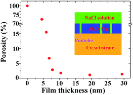
The porosity of ultra-thin alumina (Al2O3) films was determined by electrochemical measurements. The Al2O3 films were prepared by atomic layer deposition (ALD) on a copper substrate using trimethyl aluminum and water as the precursors. The copper substrate was fine-polished to decrease the influence of any surface defects on the porosity. 30 to 300 ALD cycles were performed to obtain films with a thickness in the range 4.5–29.4 nm. Auger electron spectroscopy results revealed that the Al2O3 films prepared by ALD were stoichiometric and showed low substrate sensitivity. The results obtained by potentiodynamic polarization showed that the porosity of the Al2O3 films decreased with film thickness. However, when the film thickness increased to 7.8 nm, the film porosity became stable. With further increases in the film thickness, the porosity decreased slowly. The copper substrate was well protected as a result of the low porosity of the 7.8 nm Al2O3 film. No obvious corrosion was observed in the scanning electron microscopy images.


1. Introduction

Thin films are widely used in micro-device applications as a good alternative to bulk materials. As the size of micro-devices continues to shrink, film thicknesses are being progressively driven to their limits. For example, in complementary metal oxide semiconductors and dynamic random access memory applications, high dielectric constant (high-k) oxide films with thicknesses <10 nm are used to provide sufficient capacitance.1–3 As the feature size of integrated circuits is scaled down to <32 nm, a diffusion barrier of thickness <5 nm is required to prevent copper from diffusing into the low-k materials.4 To increase the magnetic storage density to >1 Tbit/in2, the thickness of protective diamond-like carbon films should be as thin as 1–2 nm.5,6 With continued shrinking of the film thicknesses to just a few nanometers, the film may become discontinuous and the massive pinhole defects formed in the initial period of film growth remain in the film, which may lead to the failure of the device. Therefore, a knowledge of the critical thickness at which films become continuous and compact is of great significance in the normal operation of many devices.

Alumina (Al2O3) is a technologically important material due to its excellent insulation properties, high chemical and thermal stabilities, high mechanical strength and high corrosion resistance.7 As a result of these properties, Al2O3 films are widely used in micro-devices as high-k dielectric layers,1–3,8 diffusion barrier layers4,9–12 and protective coatings. Ultra-thin Al2O3 films can be deposited by an atomic layer deposition (ALD) process.13,14 In the ALD process, two precursor gases are pulsed onto a substrate surface alternately and, between the precursor pulses, the reaction chamber is purged with an inert gas. The self-limiting growth mechanism of the ALD process enables a precision thickness to be controlled at a monolayer level. Moreover, excellent step coverage, conformal deposition on high aspect ratio structures, and nearly pinhole-free and uniform composition control are obtained.

Electrochemical measurements (linear-scan voltammetry and electrochemical impedance spectroscopy) have been used to determine the porosity of ultra-thin Al2O3 films grown by thermal ALD.15–17 However, because of scratches due to polishing and particle contamination on the substrate surface, the resulting porosity of ultra-thin Al2O3 films may be overestimated.18,19 H2–Ar plasma pre-treatment has been used to remove organic contamination of the substrate.20,21 After pre-treatment, the influence of the substrate on the porosity can be eliminated to some extent and the film porosity decreased by 1–3 orders of magnitude. However, the influence of scratches on the substrate surface on the porosity still exists and the elimination of the influence of these scratches was studied in the work reported here.

Potentiodynamic polarization measurement was used to obtain the porosity of ultra-thin Al2O3 films prepared by ALD on a copper substrate. Based on the analysis of films with a thickness of 4.5–29.4 nm, the critical thickness at which the films became continuous and compact was determined. Because defects and contaminations on the surface of the copper substrate may give rise to the failure of the Al2O3 films, the copper substrate was fine-polished to decrease the surface defects.

2. Experimental methods

2.1. Surface preparation

A copper sample (99.99 wt% purity) of size 20 × 20 × 2 mm3 was used as the substrate to grow ultra-thin Al2O3 films. The copper substrate was mechanically polished using a TegraPol instrument (Struers) with silicon carbide (SiC) foils (grit size #320, #500 and #1200) as the grinding media. Chemical mechanical polishing was then used to further decrease the surface roughness. A commercial slurry (PL-7105, Fujimi) consisting of chemical reagents and submicron-sized abrasive particles was used in the chemical mechanical polishing process. Before use, the slurry was diluted with deionized water at a dilution ratio of 1[thin space (1/6-em)]:[thin space (1/6-em)]3. The substrate was finally cleaned with ultrasonic deionized water in a water-bath for 2 min and then blow-dried with pure nitrogen (99.99%).

2.2. Films prepared by atomic layer deposition

Al2O3 films were deposited on the copper substrate using a Picosun SUNALE R-150 ALD reactor. The precursors used were trimethyl aluminum (purity >99.99%) and water, which were kept at room temperature.14,22 These two precursors were alternately pulsed into a reaction chamber with high-purity nitrogen (purity >99.999%) as a carrier gas. The reaction chamber was purged with high-purity nitrogen between the precursor pulses. The flow-rates of the carrier gas and purge gas were both 150 cm3 min−1. One complete ALD cycle consisted of 0.1 s of trimethyl aluminum/N2, 3 s of N2, 0.1 s of H2O/N2 and 4 s of N2. A long purge time was adopted to prevent the two precursors reacting. By adjusting the number of ALD cycles, ultra-thin Al2O3 films of various thicknesses were obtained. During deposition, the pressure in the chamber was kept at about 14 hPa using a dry pump and the temperature in the chamber was limited to 150 °C to avoid the oxidization of the copper substrate. After preparation, the samples were stored in a vacuum drier.

The thickness of the Al2O3 films was measured from a silicon wafer that was coated at the same time as the copper substrate. Before deposition, the Si (100) substrate was cleaned in ultrasonic acetone, absolute alcohol and deionized water baths for 10 min each. The film thickness was measured by null ellipsometry (Multiskop instrument, Optrel) under ambient air. The wavelength of the Nd–YAG laser was 632.8 nm and the incidence was 70°. Modeling was performed using Elli software (Optrel). A two-layer model (air/substrate) was used to determine the refractive index and absorption coefficient of the substrate. The thickness of the Al2O3 film was then calculated using a three-layer model (air/film/substrate).

Because the thickness of the Al2O3 films was measured from the Si (100) substrate, the question arises as to whether the thickness values measured were consistent with those measured from the copper substrate. To answer this question, elemental depth profiles were obtained for the Si (100) and copper substrates coated with the Al2O3 film using Auger electron spectroscopy (AES, PHI-700, ULVAC-PHI) with a coaxial cylindrical mirror analyzer. The spectrometer was operated at a pressure of <3.9 × 10⁻⁹ Torr. The depth profiling was performed with a 5 kV Ar ion sputter beam at an incident angle of 30°. The sputtering rate of an SiO2 film (calibration specimen) was 6 nm min−1.

2.3. Electrochemical measurements

The electrochemical measurements were carried out with an M237A potentiostat (EG&G) with a three-electrode cell. A platinum wire was used as the counter electrode and a silver/silver chloride (Ag/AgCl) electrode as the reference electrode. The area of the working electrode was restricted to 2.01 cm2 by an O-ring. The electrolyte solution was 0.1 M NaCl prepared with ultra-pure water (resistivity >18 MΩ cm) and reagent-grade chemicals (NaCl Analar Normapur analytical reagent, Sinopharm Chemical Reagent Co). Before the electrochemical measurements, the open circuit potential was stabilized for 30 min. The electrochemical polarization tests were then performed at a scan rate of 2 mV s−1 from −0.25 to 0.3 V with respect to the open circuit potential.

2.4. Porosity evaluation

Fig. 1 shows a diagram of the copper coated with Al2O3 film system immersed in 0.1 M NaCl solution. Pinhole defects appear in the Al2O3 film. The NaCl solution can permeate the film at these sites and reach the copper substrate. Therefore corrosion of the substrate occurs. By comparing the corrosion of the copper substrate before and after coating with the Al2O3 film, the porosity of the Al2O3 film can be measured quantitatively. Several methods have been adopted to calculate the porosity of the film.15,21,23–25 In our study, a comparison was made of the polarization resistances of the uncoated and coated samples:25
 
image file: c4ra04565c-t1.tif(1)
where P is the porosity of the Al2O3 film, Rps is the polarization resistance of the copper substrate, Rp is the polarization resistance of the copper coated with the Al2O3 film, ΔEcorr is the difference in free corrosion potential between the coated copper and the bare copper substrate and ba is the anodic Tafel slope of the copper substrate. The corrosion potential, Ecorr, the corrosion current density, icorr, the anodic Tafel slope, ba, and cathodic Tafel slope, bc, can be obtained using the Tafel extrapolation method from the polarization curves.26 The Tafel lines are obtained from the linear portion of the polarization curves and the corrosion current density is obtained from the intersection of the Tafel lines at the corrosion potential. The polarization resistance is then obtained using the Stern–Geary equation27
 
image file: c4ra04565c-t2.tif(2)

image file: c4ra04565c-f1.tif
Fig. 1 Diagram of copper coated with Al2O3 film system immersed in 0.1 M NaCl solution.

2.5 Surface analysis

The surface morphologies of the samples before and after the electrochemical measurements were observed using atomic force microscopy (AFM, Veeco) and scanning electron microscopy (SEM, FEI Quanta 200 FEG) operating at a 20 kV accelerating voltage. The composition of the corroded copper surface was determined by X-ray photoelectron spectroscopy (XPS, PHI Quantera SXM). The binding energy was calibrated by taking the carbon C1s peak (284.8 eV) as the reference peak.

3. Results and discussion

3.1 Substrate surface

Fig. 2a shows the SEM image of the surface of the polished copper substrate. Unlike the substrates used in previously published work,17 the copper substrate shows no obvious defects; this will reduce the influence of the surface defects on the film porosity. The grain boundary of the polycrystalline copper substrate is visible, although it is not clear. Fig. 2b shows an AFM image of the polished copper substrate. The surface of the copper substrate is very smooth and the root-mean-square roughness of the surface is 0.72 nm. Because of the high z-resolution of the AFM, the grain boundary can be clearly seen. Fig. 2c is a cross-sectional profile of the copper substrate shown in Fig. 2b as a blue line. The segment between the two green dashed lines (the two green crosses in Fig. 2b) is the grain boundary. It can be seen that the depth of the grain boundary is about 2 nm. This explains why the grain boundary cannot be seen clearly by SEM.
image file: c4ra04565c-f2.tif
Fig. 2 (a) SEM image of the polished copper substrate. Black arrow = grain boundary. (b) AFM image of the polished copper substrate. Black arrow = grain boundary. (c) Cross-sectional profile of the copper substrate indicated in (b) as a blue line; the segment between the two green dashed lines is the grain boundary.

3.2 Film thickness

The growth behavior of the ALD Al2O3 films was investigated by ellipsometry. Between 30 and 300 ALD cycles were performed to obtain ultra-thin Al2O3 films of different thicknesses. Fig. 3 shows the film thickness of Al2O3 as a function of the number of ALD cycles. Each value in the figure is an average of six points measured at different locations in the sample. The film thicknesses were almost linear with respect to the number of ALD cycles, which indicates the self-limiting growth mechanism of the ALD process.
image file: c4ra04565c-f3.tif
Fig. 3 Thickness of the Al2O3 films as a function of the number of ALD cycles.

AES was used to determine whether the Al2O3 films deposited on the Si (100) substrate have the same thickness as those deposited on the copper substrate. Fig. 4a and b show the depth profiles of the Al2O3 films deposited with 200 ALD cycles on the copper and Si (100) substrates, respectively. As a result of exposure to the ambient air, a high concentration of C can be observed on the surface of the Al2O3 film. For the Al2O3 films deposited on both substrates, plateaus of O and Al are observed, which indicates that the films have a uniform in-depth stoichiometry. Moreover, for both samples, the concentrations of Al and O decrease after about 4.5 min of sputtering, which shows that the two Al2O3 films deposited on the copper and Si (100) substrates have the same film thickness.


image file: c4ra04565c-f4.tif
Fig. 4 Depth profiles of the Al2O3 film deposited with 200 ALD cycles on the (a) copper and (b) Si (100) substrates.

3.3 Electrochemical polarization

Fig. 5a shows the polarization curves for the copper substrate and the Al2O3 film coated substrate. Several electrochemical parameters, such as the corrosion potential (Ecorr), the corrosion current density (icorr), the anodic Tafel slope (ba) and the cathodic Tafel slope (bc) were determined from the polarization curves (Table 1). The corrosion potential of the bare substrate is −0.113 V (Ag/AgCl). However, the corrosion potentials shifted anodically in the coated samples. With increasing Al2O3 film thickness, the corrosion potential became more anodic, which shows an enhanced corrosion resistance. The corrosion current densities of the samples coated with Al2O3 film are significantly smaller than that of the copper substrate; the corrosion current densities of the Al2O3 film coated samples reduced by one order of magnitude with an increase in film thickness from 4.5 to 7.8 nm. When the thickness of the Al2O3 films increased further, the corrosion current became stable.
image file: c4ra04565c-f5.tif
Fig. 5 (a) Polarization curves for the copper substrate and Al2O3 film coated samples in 0.1 M NaCl solution. (b) Porosities of the samples coated with Al2O3 film.
Table 1 Electrochemical polarization data of copper substrate and Al2O3 film coated samples
Sample Ecorr (V) icorr (A cm−2) ba (V/dec) bc (V/dec) Rp (Ω cm2)
Cu −0.113 5.37 × 10⁻⁷ 0.148 0.065 3.66 × 10⁴
4.5 nm Al2O3 −0.108 3.19 × 10⁻⁷ 0.042 0.132 4.38 × 10⁴
5.9 nm Al2O3 −0.117 1.15 × 10⁻⁷ 0.062 0.165 2.21 × 10⁵
6.8 nm Al2O3 −0.099 4.33 × 10⁻⁸ 0.060 0.162 4.37 × 10⁵
7.8 nm Al2O3 −0.087 2.29 × 10⁻⁸ 0.059 0.184 8.54 × 10⁵
10.4 nm Al2O3 −0.075 1.80 × 10⁻⁸ 0.069 0.157 1.16 × 10⁶
19.4 nm Al2O3 −0.057 1.59 × 10⁻⁸ 0.076 0.141 1.35 × 10⁶
29.4 nm Al2O3 −0.048 2.99 × 10⁻⁸ 0.111 0.164 9.60 × 10⁵


The corrosion resistance of the samples coated with Al2O3 film is related to the film porosity. The porosity of the samples coated with Al2O3 film is obtained from eqn (1), whereas the polarization resistance (Rp) is calculated from eqn (2) using the electrochemical parameters listed in Table 1. The porosity of the samples coated with Al2O3 film as a function of the film thickness is shown in Fig. 5b. It can be seen that the porosity of the samples coated with Al2O3 film decreases with increasing film thickness, which explains the decrease in the corrosion current density with film thickness. The decreased porosity of the Al2O3 films is due to the progressive sealing of the defects formed in the initial period of film growth. The porosity of a 7.8 nm thick Al2O3 film is 2.86%. The porosity tends to become stable with increasing film thickness. The corrosion current density of the samples coated with Al2O3 film therefore becomes stable.

It should be mentioned that the porosities of the Al2O3 films with thicknesses of 5.9 and 10.4 nm are 15.53 and 1.74%, much lower than the previously reported 35.48% (5 nm thick Al2O3 film) and 31.45% (10 nm thick Al2O3 film).16 The low film porosity is due to the reduced surface defects on the copper substrate. In our study, the copper substrate was fine-polished to decrease the density of the surface defects, which enabled the Al2O3 films to nucleate uniformly on the surface of the copper substrate. As the influence of surface defects on the growth of the Al2O3 films was eliminated in our study, the measured porosities are more accurate.

Fig. 6a and b show the SEM images of the copper substrate after corrosion. The copper substrate corrodes severely and a large amount of bamboo-like structures appear on the copper surface. Similar structures have been observed in previously published work.28 The copper substrate is corroded uniformly because the bamboo-like structures are distributed uniformly. Fig. 7a–c show the XPS spectra of Cu 2p, O 1s and Cl 2p core levels of the corroded copper substrate, respectively. The peak position of the Cu 2p core level appears at 932.8 eV, which may be ascribed to the presence of CuCl or Cu2O.29–31 These two possibilities cannot be distinguished from one another as a result of their close binding energy. The O 1s peak at 530.8 eV is due to the presence of Cu2O29 and the Cl 2p peaks at 198.9 and 200.5 eV are due to the presence of CuCl.31 The existence of the O 1s and Cl 2p peaks shows that both CuCl and Cu2O are formed during the corrosion process. The overall reaction of the copper in the NaCl solution is as follows:32

 
Cu = Cu+ + e (3)
 
Cu+ + Cl = CuCl (4)
 
2CuCl + H2O = Cu2O + 2H+ + 2Cl (5)


image file: c4ra04565c-f6.tif
Fig. 6 (a) SEM image of the copper substrate after electrochemical polarization measurements. (b) Magnified image of (a). (c) SEM image of the copper substrate coated with a 4.5 nm Al2O3 film after electrochemical polarization measurement. (d) Magnified image of (c). (e) SEM image of the copper substrate coated with a 7.8 nm Al2O3 film after electrochemical polarization measurement. (f) Magnified image of (e).

image file: c4ra04565c-f7.tif
Fig. 7 XPS spectra of (a) Cu 2p, (b) O 1s and (c) Cl 2p core levels of the corroded copper substrate.

Fig. 6c and d are images of the copper substrate coated with a 4.5 nm thick Al2O3 film after corrosion. As a result of the high porosity of the 4.5 nm Al2O3 film, bamboo-like structures can also be observed, but the amount of bamboo-like structures is decreasing. Fig. 6e and f show the images of the copper substrate coated with the 7.8 nm Al2O3 film after corrosion. As a result of the low porosity of the 7.8 nm Al2O3 film, the copper substrate is well protected. Only local corrosion occurs, which is revealed on the image as spots. The local corrosion behavior confirms the fact that the corrosion is caused by pinhole defects.

4. Conclusions

Electrochemical measurements were performed to determine the porosity of the ultra-thin Al2O3 films prepared by ALD. Because the surface of the copper substrate was fine-polished, the influence of the surface defects on the film porosity was to some extent eliminated and the resulting porosity was smaller than that obtained in previous studies. The AES results show that the Al2O3 films are stoichiometric and that the Al2O3 films deposited on the copper substrate have the same thickness as those deposited on the Si (100) substrate. The porosity of the Al2O3 films obtained from potentiodynamic polarization shows a decrease in the porosity with increasing film thickness from 77.20 to 1.39% for the 4.5 and 29.4 nm Al2O3 films, respectively. However, when the film thickness increased to 7.8 nm, the porosity value became stable. As the film thickness increased further, the porosity decreased slowly. As a result of the low porosity, the surface of the copper substrate coated with a 7.8 nm Al2O3 film is not severely corroded, as confirmed by SEM. The method in this study could be used to measure the porosity of other insulated ultra-thin films.

Acknowledgements

The authors greatly appreciate the financial support of the National Science Fund for Distinguished Young Scholars (50825501), the Science Fund for Creative Research Groups (51321092), the National Natural Science Foundation of China (51335005), and the National Science and Technology Major Project (2008ZX02104-001). Helpful discussions with Wen Jing are gratefully acknowledged.

Notes and references

  1. S. K. Kim, G. J. Choi, S. Y. Lee, M. Seo, S. W. Lee, J. H. Han, H. S. Ahn, S. Han and C. S. Hwang, Adv. Mater., 2008, 20, 1429 CrossRef CAS PubMed.
  2. C. H. Chang, Y. K. Chiou, C. W. Hsu and T. B. Wu, Electrochem. Solid-State Lett., 2007, 10, G5 CrossRef CAS PubMed.
  3. J. Niinisto, K. Kukli, M. Heikkila, M. Ritala and M. Leskela, Adv. Eng. Mater., 2009, 11, 223 CrossRef CAS PubMed.
  4. C. C. Chang and F. M. Pan, J. Electrochem. Soc., 2011, 158, G97 CrossRef CAS PubMed.
  5. Z. Min, Z. Chenhui, L. Jianbin and L. Xinchun, Appl. Surf. Sci., 2009, 256, 322 CrossRef PubMed.
  6. C. Casiraghi, J. Robertson and A. C. Ferrari, Mater. Today, 2007, 10, 44 CrossRef CAS.
  7. M. D. Groner, J. W. Elam, F. H. Fabreguette and S. M. George, Thin Solid Films, 2002, 413, 186 CrossRef CAS.
  8. C. C. Cheng, C. H. Chien, G. L. Luo, J. C. Liu, C. C. Kei, D. R. Liu, C. N. Hsiao, C. H. Yang and C. Y. Changa, J. Electrochem. Soc., 2008, 155, G203 CrossRef CAS PubMed.
  9. P. Majumder, R. Katamreddy and C. Takoudis, Electrochem. Solid-State Lett., 2007, 10, H291 CrossRef CAS PubMed.
  10. T. Cheon, S. H. Choi, S. H. Kim and D. H. Kang, Electrochem. Solid-State Lett., 2011, 14, D57 CrossRef CAS PubMed.
  11. C. Taehoon, C. Sang-Hyeok, K. Soo-Hyun and K. Dae-Hwan, Electrochem. Solid-State Lett., 2011, 14, D57 CrossRef PubMed.
  12. S. I. Song, J. H. Lee, B. H. Choi, H. K. Lee, D. C. Shin and J. W. Lee, Surf. Coat. Technol., 2012, 211, 14 CrossRef CAS PubMed.
  13. R. L. Puurunen, J. Appl. Physiol., 2005, 97, 121301 CrossRef PubMed.
  14. M. Juppo, A. Rahtu, M. Ritala and M. Leskela, Langmuir, 2000, 16, 4034 CrossRef CAS.
  15. B. Diaz, E. Harkonen, J. Swiatowska, V. Maurice, A. Seyeux, P. Marcus and M. Ritala, Corros. Sci., 2011, 53, 2168 CrossRef CAS PubMed.
  16. B. Diaz, J. Swiatowska, V. Maurice, A. Seyeux, B. Normand, E. Harkonen, M. Ritala and P. Marcus, Electrochim. Acta, 2011, 56, 10516 CrossRef CAS PubMed.
  17. B. Diaz, E. Harkonen, V. Maurice, J. Swiatowska, A. Seyeux, M. Ritala and P. Marcus, Electrochim. Acta, 2011, 56, 9609 CrossRef CAS PubMed.
  18. Y. D. Zhang, D. Seghete, A. Abdulagatov, Z. Gibbs, A. Cavanagh, R. G. Yang, S. George and Y. C. Lee, Surf. Coat. Technol., 2011, 205, 3334 CrossRef CAS PubMed.
  19. A. I. Abdulagatov, Y. Yan, J. R. Cooper, Y. Zhang, Z. M. Gibbs, A. S. Cavanagh, R. G. Yang, Y. C. Lee and S. M. George, ACS Appl. Mater. Interfaces, 2011, 3, 4593 CAS.
  20. E. Harkonen, S. E. Potts, W. Kessels, B. Diaz, A. Seyeux, J. Swiatowska, V. Maurice, P. Marcus, G. Radnoczi, L. Toth, M. Kariniemi, J. Niinisto and M. Ritala, Thin Solid Films, 2013, 534, 384 CrossRef CAS PubMed.
  21. S. E. Potts, L. Schmalz, M. Fenker, B. Diaz, J. Swiatowska, V. Maurice, A. Seyeux, P. Marcus, G. Radnoczi, L. Toth and W. Kessels, J. Electrochem. Soc., 2011, 158, C132 CrossRef CAS PubMed.
  22. A. W. Ott, K. C. McCarley, J. W. Klaus, J. D. Way and S. M. George, Appl. Surf. Sci., 1996, 107, 128 CrossRef CAS.
  23. W. Tato and D. Landolt, J. Electrochem. Soc., 1998, 145, 4173 CrossRef CAS PubMed.
  24. C. Liu, Q. Bi, A. Leyland and A. Matthews, Corros. Sci., 2003, 45, 1257 CrossRef CAS.
  25. V. Grips, V. E. Selvi, H. C. Barshilia and K. S. Rajam, Electrochim. Acta, 2006, 51, 3461 CrossRef CAS PubMed.
  26. E. McCafferty, Corros. Sci., 2005, 47, 3202 CrossRef CAS PubMed.
  27. M. Stern and A. L. Geary, J. Electrochem. Soc., 1957, 104, 56 CrossRef CAS PubMed.
  28. L. Wei, X. Yimin, W. Qiming, S. Peizhen and Y. Mi, Corros. Sci., 2010, 52, 3509 CrossRef PubMed.
  29. S. L. Shinde and K. K. Nanda, RSC Adv., 2012, 2, 3647 RSC.
  30. N. S. Mcintyre and M. G. Cook, Anal. Chem., 1975, 47, 2208 CrossRef CAS.
  31. R. P. Vasquez, Surf. Sci. Spectra, 1993, 2, 138 CrossRef CAS.
  32. A. El Warraky, H. A. El Shayeb and E. M. Sherif, Anti-Corros. Methods Mater., 2004, 51, 52 CrossRef CAS.

This journal is © The Royal Society of Chemistry 2014
Click here to see how this site uses Cookies. View our privacy policy here.