Long-term air-stable n-type doped graphene by multiple lamination with polyethyleneimine
Myoung-Jun Chaa,
Wooseok Songc,
Yooseok Kimad,
Dae Sung Jungb,
Min Wook Jungac,
Su Il Leea,
Prashanta Dhoj Adhikaria,
Ki-Seok Anc and
Chong-Yun Park*ab
aDepartment of Physics, Sungkyunkwan University, Suwon 440-746, Republic of Korea. E-mail: cypark@skku.edu
bDepartment of Energy Science, Sungkyunkwan University, Suwon 440-746, Republic of Korea
cThin Film Materials Research Group, Korea Research Institute of Chemical Technology, Yuseong Post Office Box 107, Daejeon 305-600, Republic of Korea
dDivision of Material Science, Korea Basic Science Institute, Daejeon 305-333, Republic of Korea
First published on 4th August 2014
Abstract
We demonstrate homogeneous and air-stable n-type doping of graphene grown by thermal chemical vapor deposition. Laminated Polyethyleneimine (PEI) layers fabricated by a simple polymer solution coating were employed. The doping stability of multiple laminated structures (graphene/PEI, PEI/graphene, and graphene/PEI/graphene) was systematically investigated. The resulting graphene/PEI/graphene laminated structure was highly stable in air. Moreover, the work function and carrier concentration of doped graphene can be tuned by altering the laminated structure.
1. Introduction
Graphene has recently received a great deal of attention due to its unique properties associated with massless Dirac fermions, such as its ultra-high electrical conductivity, anomalous quantum Hall effect, and Klein tunneling.1–4 Graphene also has exceptional physical properties, including excellent optical transparency, mechanical strength, and chemical stability. The facile fabrication of large-area graphene films via chemical vapor deposition (CVD) and wet transfer processes makes it one of the most promising materials for potential uses in next-generation nanoelectronics.5–10Conventional metal and metal oxide electrodes possess low stability in dye sensitized solar cells and organic light emitting diodes due to the acidity or alkalinity of contact materials. The electrodes also exhibit low efficiency due to Schottky contact between electrodes and contact materials induced by their work function difference. Conversely, graphene has a high chemical stability due to strong C–C covalent bonds and good Ohmic contact caused by the low electronic density of states near the Fermi level.7 To obtain both high- and low-work function graphene, several approaches that control the charge carrier densities of graphene have been studied. Homogeneous and stable p-type doping of graphene has been achieved. However, n-type doping approaches are unstable in atmospheric conditions due to electron withdrawing by adsorbed charged impurities, such as oxygen and water molecules.8 Recently, n-type doping of graphene has been conducted using covalent and non-covalent bonding approaches.9–14 The covalent bonding approach involves atomic substitution of dopants in graphene, resulting in destruction of the graphene structure accompanied by doping concentration.15 The non-covalent approach manipulates the π-orbital electronic structure of graphene using lamination of metal oxides or functional groups without destruction of the graphene structure.16 Self-assembled monolayers (SAMs) represent a non-covalent method using polarized functional groups. Using SAMs, the type and concentration of carriers can be controlled by spacer group length and end group polarity. However, the substrates are limited by different chemical reactions.17 Alternatively, non-covalent dopants, aromatic compounds, and polymers have been employed for graphene doping. These materials are suitable for solution processing and enable graphene to form substrate-independently.9,10,18 Among these materials, polyethylenimine (PEI) film contains a high density of primary, secondary, and tertiary amine groups, and has chemical stability in ambient conditions.
In this study, we demonstrated the homogeneous and air-stable n-type doping of graphene by lamination with solution processed branched-PEI film. The graphene work function was tuned by lamination of the PEI film. The structure of laminated layers was optimized in terms of homogeneous and air stable n-type doping of graphene.
2. Experimental details
2.1 Chemical vapor deposition synthesis of graphene
Graphene was synthesized by thermal CVD (TCVD). First, a 25 μm-thick Cu foil (99.8% purity and Alfa Aesar) was annealed at 1050 °C with H2 gas flowing at 100 sccm for 2 hours to remove the native Cu oxide layer, enlarge Cu grains, and establish a smooth surface. Graphene was synthesized at 1050 °C by introducing CH4 (5 sccm) together with H2 (20 sccm) for 30 min. After turning off the flow of CH4, the TCVD reactor was cooled down to room temperature with Ar.2.2 Transfer process for graphene
Graphene was transferred onto desired substrates (300 nm-thick SiO2/Si (001) and polyethylene terephthalate (PET)) by a poly(methylmethacrylate) (PMMA)-assisted wet-transfer method.19 The PMMA dissolved in chlorobenzene was spin-coated onto graphene/Cu at 1000 rpm for 15 s, followed by curing at 90 °C for 5 min. The PMMA-coated graphene/Cu was placed in Cu etchant (CE-100, Transene Company, Inc.) to remove the Cu foil. After the Cu foil was completely etched away, PMMA-coated graphene was scooped from the etchant using the desired substrates. The PMMA layer was then removed with acetone, and the sample was rinsed several times with DI water.2.3 Fabrication of PEI layer
A branched PEI with a molecular weight of 750![[thin space (1/6-em)]](https://www.rsc.org/images/entities/char_2009.gif) 000 g mol−1 was purchased from Sigma Aldrich. A 0.1 wt% branched-PEI was dissolved in methyl alcohol. Aqueous ammonia solution was used as an additive to maintain a pH of 9. This solution was spin-coated onto graphene/SiO2/Si or SiO2/Si at 2500 rpm for 1 min. After spin-coating, the sample was heated at 80 °C for 2 min to remove solvent.
000 g mol−1 was purchased from Sigma Aldrich. A 0.1 wt% branched-PEI was dissolved in methyl alcohol. Aqueous ammonia solution was used as an additive to maintain a pH of 9. This solution was spin-coated onto graphene/SiO2/Si or SiO2/Si at 2500 rpm for 1 min. After spin-coating, the sample was heated at 80 °C for 2 min to remove solvent.
3. Results and discussion
The structural characteristics of graphene laminated with PEI thin film were analyzed by optical microscopy, atomic force microscopy (AFM), and scanning electron microscopy (SEM). Fig. 1 shows the optical microscopy, AFM, and SEM images of graphene before (Fig. 1(a) and (b)) and after (Fig. 1(c)–(f)) PEI coating. After PEI coating, a uniform surface without residues was formed. The root mean square (RMS) roughness obtained from graphene before and after PEI coating is 2.473 and 1.243 nm, respectively. An ultrathin PEI layer (<5 nm) coated on the graphene was observed. These results indicate that PEI/graphene was formed with an ultra-flat and defect-free surface. This process is better than nanoparticle-mediated doping processes for preparing transparent and flexible electrodes with optical transmittance uniformity. | ||
| Fig. 1 Optical microscope and AFM images of (a) and (b) before and (c) and (d) after PEI-coating on graphene (PGS). SEM images of (e) top view and (f) tilted view. | ||
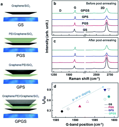
To optimize the doping concentration and stability, four different laminated structures were established: graphene/SiO2 (GS), PEI/graphene/SiO2 (PGS), graphene/PEI/SiO2 (GPS), and graphene/PEI/graphene/SiO2 (GPGS). The electrical interaction between graphene and the PEI film was investigated by resonant Raman spectroscopy with an excitation wavelength of 514 nm. Fig. 2(b) and (c) show the Raman spectra of GS, PGS, GPS, and GPGS, which demonstrate the graphene characteristics of the D-band (∼1355 cm−1), G-band (∼1588 cm−1), and 2D-band (∼2689 cm−1). The D-band is absent for GS and the intensity ratio of 2D- to G-bands (I2D/IG) is 0.34, indicating that high crystalline monolayer graphene was synthesized. In all Raman spectra, no noticeable changes in the D-band are observed, reflecting that structural deformation of graphene was absent after the formation of the graphene/PEI laminated structure. Fig. 2(d) shows the G-band position and IG/I2D of GS, PGS, GPS, and GPGS before and after post-annealing. A blueshift of the G-band and a significant increase in IG/I2D are both observed after the formation of graphene/PEI laminated structures, indicating that n-type doping occurred by electron charge transfer from PEI to graphene.18 Because a branched PEI contains a large number of amine (NH2) group, n-type doped graphene due to the electron donating characteristics of the amine group was formed. After post-annealing GS, the doping effect was significantly degraded by removing ambient p-type dopants, such as oxygen and water molecules. PGS de-doping was also observed after post-annealing, presumably due to a chemical composition change in the PEI layer. The doping concentrations of GPS and GPGS were greater than those of GS and PGS. GPS and GPGS doping was stable after post-annealing, likely due to the graphene protective layer maintaining the chemical composition of the PEI layer.
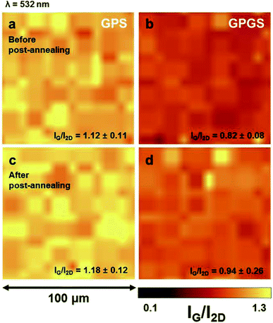
Uniformity was evaluated in terms of doping concentration by confocal Raman mapping of IG/I2D values (100 μm × 100 μm), as shown in Fig. 3. Based on the Raman maps, the average IG/I2D values of GPS and GPGS are 1.12 and 0.82, respectively. All standard deviations are below 0.11. After post-annealing, the average IG/I2D values of GPS and GPGS were maintained. These Raman maps exhibit excellent uniformity over large areas, presumably due to homogeneous n-type doping.
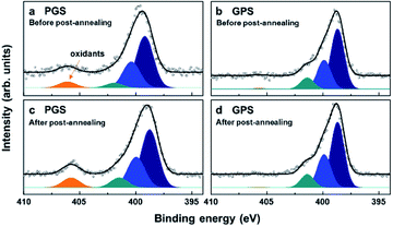
The chemical states of the graphene/PEI laminated structure were systematically investigated using X-ray photoelectron spectroscopy (XPS). XPS spectra were acquired with normal emission geometry using conventional monochromatic Al Kα radiation (hν = 1486.6 eV). The N 1s core level spectra obtained from PGS and GPS before and after post-annealing at 120 °C are shown in Fig. 4(a)–(d). Spectra were deconvoluted by a standard nonlinear-least-squares fitting procedure using Voigt functions. The N 1s peaks of PEI (amine group) located at binding energy (EB) = 403.3 eV, 398.9 eV, and 396.9 eV were observed. For PGS, an oxidant peak (N–O species, EB = 406.6 eV) was observed that increased after post-annealing. These results suggest that the PEI layer was not oxidized for GPS because capped graphene prevents ambient oxidation by high chemical stability and gas barrier properties.19
 | ||
| Fig. 4 XPS N 1s core level spectra of PGS and GPS (a and b) before and (c and d) after post-annealing. | ||
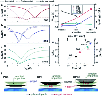
To examine the electrical transport of graphene/PEI laminated structures, electrochemically gated graphene/PEI FETs were fabricated. InSn and 1-buty-3-methylimidazolium (BmimPF6) were used as the source/drain electrodes and ionic liquid.20 Fig. 5(a)–(c) show transfer curves (IDS–VG) at VDS = 0.1 V for PGS, GPS, and GPGS before (as-coated) and after the post-annealing (post-annealed), remaining in air for one month. A charge-neutral Dirac point of graphene (VCNP), defined as the minimum point of source/drain current (IDS), was generally observed in the transfer curve due to the low density of states near the Fermi level.7 As a result of n-type doping effects from laminating the PEI layer, all graphene-PEI laminated structures showed negative gate voltage (VG) of VCNP (PGS (−0.72 V), GPS (−0.88 V), and GPGS (−0.68 V)). However, the PGS VCNP shifted toward positive VG after post-annealing and remaining in air for one month. This is due to degradation of the doping effect of PEI via oxidation, as shown in Fig. 5(a).21 For GPS and GPGS, the VCNP was maintained after post-annealing due to a graphene protective layer maintaining the chemical composition of the PEI layer. Samples were placed in air for one month and then re-measured to verify their long-term stability. Results indicated that the VCNP of GPS and GPGS were −0.02 V and −0.77 V, respectively. The VCNP for PGS, GPS, and GPGS before and after post-annealing and remaining in air for one month was plotted in Fig. 5(d). Remarkably, the GPGS structure is highly stable in air. Fig. 5(e) shows the relationship of the IG/I2D, work function (WG), VCNP, and carrier concentration (n) of graphene/PEI laminated structures. n in doped graphene was calculated by the relationship,
where C′, γep and EF are the constant value, phonon emission, and Fermi energy, respectively.23 For GPGS and GPS, highly n-type doped graphene was formed, as confirmed by the IG/I2D and VCNP. Notably, this result indicates that the WG and n of graphene can be tuned by altering the laminated structure. Consequently, the GPGS laminated structure was optimized in terms of homogeneous and air stable n-type doping. For GPGS, the top graphene layer prevented ambient oxidants, resulting in maintenance of the chemical states of PEI and the bottom graphene layer, as depicted in Fig. 5(f).
4. Conclusions
A facile methodology was established for homogeneous and air-stable n-type doping of graphene through lamination of PEI layers under ambient conditions. The structure of laminated layers was optimized in terms of homogeneous and air stable n-type doping. The work function and carrier concentration of doped graphene can be tuned by altering the laminated structure. This result provides an important means for manipulating the electronic structure of graphene, which is applicable for use in future nanoelectronics.Acknowledgements
This work was supported by the Institute for Basic Science (IBS) in Korea, and the Basic Science Research Program (2013-008639) through the National Research Foundation of Korea (NRF), funded by the Ministry of Education, Science and Technology. Wooseok Song, Min Wook Jung, and Ki-Seok An were supported by a grant (2011-0031636) from the Center for Advanced Soft Electronics under the Global Frontier Research Program of the Ministry of Science, ICT and Future Planning, Korea.Notes and references
- Y. Yang, M. C. Gupta and K. L. Dudley, Nanotechnology, 2007, 18, 345701 CrossRef
.
- N. M. Gabor, J. C. W. Song, Q. Ma, N. L. Nair, T. Taychatanapat, K. Watanabe, T. Taniguchi, L. S. Levitov and P. Jarillo-Herrero, Science, 2011, 334, 648 CrossRef CAS PubMed
.
- S. Chen, L. Brown, M. Levendorf, W. Cai, S.-Y. Ju, J. Edgeworth, X. Li, C. W. Magnuson, A. Velamakanni, R. D. Piner, J. Kang, J. Park and R. S. Ruoff, ACS Nano, 2011, 5, 1321 CrossRef CAS PubMed
.
- Y.-M. Lin, C. Dimitrakopoulos, K. A. Jenkins, D. B. Farmer, H.-Y. Chiu, A. Grill and P. Avouris, Science, 2010, 327, 662 CrossRef CAS PubMed
.
- C. Lee, X. Wei, J. W. Kysar and J. Hone, Science, 2008, 321, 385 CrossRef CAS PubMed
.
- S. Bae, H. Kim, Y. Lee, X. Xu, J.-S. Park, Y. Zheng, J. Balakrishnan, T. Lei, H. R. Kim, Y. I. Song, Y.-J. Kim, K. S. Kim, B. Ozyilaz, J.-H. Ahn, B. H. Hong and S. Iijima, Nat. Nanotechnol., 2010, 5, 574 CrossRef CAS PubMed
.
- H. Yang, J. Heo, S. Park, H. J. Song, D. H. Seo, K.-E. Byun, P. Kim, I. K. Yoo, H.-J. Chung and K. Kim, Science, 2012, 336, 1140 CrossRef CAS PubMed
.
- A. Pirkle, J. Chan, A. Venugopal, D. Hinojos, C. W. Magnuson, S. McDonnell, L. Colombo, E. M. Vogel, R. S. Ruoff and R. M. Wallace, Appl. Phys. Lett., 2011, 99, 122108 CrossRef PubMed
.
- K. C. Kwon and K. S. Choi, J. Phys. Chem. C, 2012, 116, 26586 CAS
.
- P. Wei, N. Liu, H. R. Lee, E. Adijanto, L. Ci, B. D. Naab, J. Q. Zhong, J. Park, W. Chen, Y. Cui and Z. Bao, Nano Lett., 2013, 13, 1890 CrossRef CAS PubMed
.
- X. Wang, X. Li, L. Zhang, Y. Yoon, P. K. Weber, H. Wang, J. Guo and H. Dai, Science, 2009, 324, 768 CrossRef CAS PubMed
.
- D. Wei, Y. Liu, Y. Wang, H. Zhang, L. Huang and G. Yu, Nano Lett., 2009, 9, 1752 CrossRef CAS PubMed
.
- C. Zhang, L. Fu, N. Liu, M. Liu, Y. Wang and Z. Liu, Adv. Mater., 2011, 23, 1020 CrossRef CAS PubMed
.
- Y.-C. Lin, C.-Y. Lin and P.-W. Chiu, Appl. Phys. Lett., 2010, 96, 133110 CrossRef PubMed
.
- V. Georgakilas, M. Otyepka, A. B. Bourlinos, V. Chandra, N. Kim, K. C. Kemp, P. Hobza, R. Zboril and K. S. Kim, Chem. Rev., 2012, 112, 6156 CrossRef CAS PubMed
.
- F. Chen, J. Xia and N. Tao, Nano Lett., 2009, 9, 1621 CrossRef CAS PubMed
.
- J. Baltazar, H. Sojoudi, S. A. Paniagua, J. Kowalik, S. R. Marder, L. M. Tolbert, S. Graham and C. L. Henderson, J. Phys. Chem. C, 2012, 116, 19095 CAS
.
- H. C. P. Movva, M. E. Ramon, C. M. Corbet, S. Sonde, S. F. Chowdhury, G. Carpenter, E. Tutuc and S. K. Banerjee, Appl. Phys. Lett., 2012, 101, 183113 CrossRef PubMed
.
- S. S. Roy and M. S. Arnold, Adv. Funct. Mater., 2013, 23, 3638 CrossRef CAS PubMed
.
- J. Ye, M. F. Craciun, M. Koshino, S. Russo, S. Inoue, H. Yuana, H. Shimotani, A. F. Morpurgo and Y. Iwasa, Proc. Natl. Acad. Sci. U. S. A., 2011, 108, 13002 CrossRef CAS PubMed
.
- S. S. Sabri, J. Guillemette, A. Guermoune, M. Siaj and T. Szkopek, Appl. Phys. Lett., 2012, 100, 113106 CrossRef PubMed
.
- J. Yan, Y. Zhang, P. Kim and A. Pinczuk, Phys. Rev. Lett., 2007, 98, 166802 CrossRef
.
- C. Casiraghi, Phys. Rev. B: Condens. Matter Mater. Phys., 2009, 80, 233407 CrossRef
.
| This journal is © The Royal Society of Chemistry 2014 |


