Effect of Interface energy and electron transfer on shape, plasmon resonance and SERS activity of supported surfactant-free gold nanoparticles

Maria M. Giangregorio*a, Babak Dastmalchib, Alexandra Suvorovac, Giuseppe V. Biancoa, Kurt Hingerld, Giovanni Brunoa and Maria Losurdoa
aInstitute of Inorganic Methodologies and of Plasmas, CNR-IMIP, via Orabona 4, 70126 Bari, Italy. E-mail: michelaria.giangregorio@cnr.it
bAmes Laboratory—U.S. DOE and Department of Physics and Astronomy, Iowa State University, Ames, Iowa 50011, USA
cCentre for Microscopy, Characterisation and Analysis, The University of Western Australia, 35 Stirling Highway, Crawley 6009 WA, Australia
dCenter for Surface- and Nanoanalytics, Johannes Kepler University Linz, Altenbergerstr. 69, 4040 Linz, Austria

Received 24th April 2014 , Accepted 23rd June 2014

First published on 23rd June 2014


Abstract

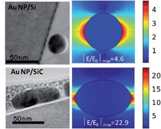
For device integration purposes plasmonic metal nanoparticles must be supported/deposited on substrates. Therefore, it is important to understand the interaction between surfactant-free plasmonic metal nanoparticles and different substrates, as well as to identify factors that drive nanoparticles nucleation and formation. Here we show that for nanoparticles grown directly on supports, the substrate/nanoparticle interfacial energy affects the equilibrium shape of nanoparticles. Therefore, oblate, spherical and prolate Au nanoparticles (NPs) with different shapes have been deposited by radiofrequency sputtering on substrates with different characteristics, namely a dielectric oxide Al2O3 (0001), a narrow bandgap semiconductor Si (100), and a polar piezoelectric wide bandgap semiconductor 4H–SiC (0001). We demonstrate that the higher the substrate surface energy, the higher the interaction with the substrate, resulting in flat prolate Au nanoparticles. The resulting localized surface plasmon resonance characteristics of Au NPs/Al2O3, Au NPs/Si and Au NPs/SiC have been determined by spectroscopic ellipsometry and correlated with their structure and shape studied by transmission electron microscopy. Finally, we have demonstrated the diverse response of the tailored plasmonic substrates as ultrasensitive SERS chemical sensors. Flat oblates Au NPs on SiC result in an enhanced and more stable SERS response. The experimental findings are validated by numerical simulations of electromagnetic fields.


Introduction

Plasmonic nanoparticles (NPs) are exploited in a broadly expanding range of technologies spanning from plasmonic circuits to catalysis1 and to nucleic acid detection.2 Those applications are enabled by the fascinating size- and shape-dependent localized surface plasmon resonance (LSPR) properties of noble metal (e.g. Au and Ag) NPs. Their high local electromagnetic fields have widened applications of Au NPs and of surface enhanced Raman spectroscopy (SERS).3 In this regard, a number of studies have focused on the control of the size,4 shape,5,6 and gaps of the NPs, i.e. particle–particle interaction.7 Many studies focus on the reduction of a dissolved gold precursor by a reducing agent in solution to create NPs, whose size and shape are controlled by solution parameters or by template-synthesis.8 Indeed, exploitation of plasmonic NPs into device applications involves depositing NPs on solid substrate supports. Therefore, chemical and physical phenomena at the substrate/NP interface deserve attention. As an example, substrate/NPs interaction can affect the NPs structure and, consequently, their optical and SERS response.9 Under external optical excitation, the substrate can also be polarized and induce a non uniform electric field across the metal NP affecting the plasmonic properties.10 Specifically, the growth of surfactant-free plasmonic nanostructures on a semiconductor breaks the symmetry of the environment; in addition, the alignment of the Fermi levels will occur by an electron transfer between the NPs and the substrate, resulting in an electric field at the substrate/NP interface.11 Importantly, the charge transfer phenomena at the substrate/NP interface have been considered as additional channels for LSPR damping, a phenomenon that is known as chemical interface damping.12 Nevertheless, it has not been duly considered that the charge transfer at the substrate/NP interface can also alter the substrate wetting by the metal NPs and consequently affect the shape of the NPs. This can be understood considering that the delocalization of electrons at the substrate/NP interface alters the adsorption and surface diffusion of Au NPs.13

In this paper, surfactant-free Au NPs are deposited directly by sputtering on substrates with different dielectric characteristics, namely the high bandgap (∼7 eV) oxide Al2O3 (0001), the narrow bandgap (1.1 eV) semiconductor Si (100), and the polar piezoelectric wide bandgap (3.3 eV) semiconductor 4H–SiC (0001). Noteworthy, 4H–SiC is a heavily doped semiconductor with high carrier mobility that is qualified as a low loss plasmonic material interesting for plasmonic around the optical frequencies, where Au NPs show their LSPR. 4H–SiC is also interesting because it presents in the infrared spectral region the so-called surface phonon polaritons (SPhPs), due to the coupling of the electromagnetic field to lattice vibrations of polar dielectrics at the infrared frequencies.14 Recently, the high potential of field enhancement by SPhP excitation for gold on SiC has been demonstrated.15

In this paper, we demonstrate and discuss how the different surface energy of the substrates drives the NPs nucleation and, consequently, shape, thereof depositing oblate, prolate and spherical Au NPs. The optical properties measured by spectroscopic ellipsometry (SE) are correlated to the NP' shape investigated by transmission electron microscopy (TEM) and rationalized by electromagnetic field maps obtained by simulations using COMSOL. Finally, the impact of the LSPR characteristics on the performance of Au NPs/Al2O3, Au NPs/Si and Au NPs/SiC systems as SERS substrates is evaluated comparatively, using as probing molecule the aromatic 4-methoxyterphenyl-3′′,5′′-dimethanethiol (TPDMT).

Experimental

Au NPs were deposited by r.f. (13.56 MHz) sputtering of a target of metallic gold using an argon plasma operated at 14 Watt and 0.3 Torr.16 Al2O3 (0001), n-type Si (100), and on-axis n-type 4H–SiC (0001) were used as substrate. They were degreased by CCl4–acetone–isopropanol, and annealed in situ in Ar at 600 °C for 10 min for contaminants desorption. The sputtering time controlled the amount of deposited gold, being the same for the three substrates.

For SERS experiments, the TPDMT thiol was used as probe molecule; the interest in this molecule is because aromatic thiols can lead to additional interaction via π-stacking to be exploited also in organic field-effect transistors (OFET)-based electronic devices.17 TPDMT was synthesized according to the details given in ref. 18. Characterization and purity of TPDMT information is detailed in ref. 17 and 18. All reactions were carried out under a nitrogen atmosphere in oven-dried glassware with dry solvents. The solvent dichloromethane was immediately distilled prior to use from phosphorus pentoxide. A fresh solution of TPDMT was prepared in anhydrous dichloromethane and stored in a Schlenk tube under a nitrogen atmosphere, and the same solution was used for all the measurements in the present work. The stability of the thiol solution was checked over a month by acquiring control Raman spectra of the solution that did not show any sulfur-oxide and/or S–S bond from interlinking over a month. We also investigated the thermal stability of the TPDMT self-assembled monolayer on gold surfaces, and our finding showed that it is stable up to a temperature of 150 °C, which is close to the melting point (TPDMT mp = 163 °C).

Samples were dipped for 1 h in 1 mM solution of TPDMT in CH2Cl2 at 25 °C and they were subsequently rinsed with CH2Cl2 solvent and dried under a N2 stream.

The compositional and structural properties were measured using a combination of high resolution transmission electron microscopy (HRTEM) and energy-filtered transmission electron microscopy (EFTEM) using a JEOL 3000F field emission gun TEM equipped with a Gatan image filter and digital camera. The chemical information was visualized by generating EFTEM images of constituent elements. To observe the elemental distribution within a Au/interface/Si stack, EFTEM images were acquired for the silicon L2,3, carbon K, oxygen K, aluminium L2,3 and gold O2,3 edges using the standard three window method and the optimum elemental mapping parameters calculated by using a reference spectrum. Cross sectional samples for TEM studies were prepared by Focussed Ion Beam (FIB) technique using an in situ lift-out method in the FEI Nova Nanolab dual-beam FIB system.

Raman and SERS spectra were acquired with a Horiba Jobin-Yvon LabRAM HR-VIS micro-Raman spectrometer using a 633 nm laser source with an incident laser power of 10 mW, using a D1 filter to reduce photobleaching. A 100× objective (numerical aperture, NA = 0.75) and acquisition time of 5 s were used for all measurements.

The LSPR properties of Au NPs were characterized by spectroscopic ellipsometry (SE) through the measurement of the extinction coefficient, k, in the range 0.75–6.5 eV by a phase modulated spectroscopic ellipsometer (UVISEL-Jobin Yvon) at an incidence angle of 70°. Although the Al2O3 (0001) and 4H–SiC (0001) substrates are uniaxial anisotropic, the optical axis is perpendicular to the sample surface; therefore, standard ellipsometry can still be applied. Furthermore, SE spectra acquired at various angles of incidence in the range 55–75° and also at various azimuth angles did not detect any significant anisotropy because of the random distribution of the self-aggregated NPs. Therefore, the data were analyzed under the isotropy assumption, and the Au NPs ensemble was parameterized with Lorentzian oscillators to derive the LSPR energy and broadening according to the approach described in ref. 19. In the present case, the size of the nanoparticles is much smaller than the wavelength of the incident light; therefore, the plasmon resonance can be approximated by polarizable electric point dipoles.

The experimental results are compared with numerical solutions obtained with a model of a nanoparticle supported on an infinite substrate constructed using the commercial COMSOL software package. The COMSOL simulations were performed with periodic boundary conditions imposed in x and y directions with a unit cell of 50 nm (an average distance between nanoparticles derived from TEM and atomic force microscopy images). The COMSOL simulations used the Johnson and Christy20 optical data for Au and the substrate was modelled using constant permittivities of n = 1.8 for Al2O3, n = 3.46 for Si, and n = 2.6 for SiC (n is the refractive index); the oblate and prolate axes aspect ratio was fixed at 1.5 consistently with the TEM data.

Results and discussion

Fig. 1 shows TEM images of Au NPs supported on Si (100), Al2O3 (0001) and 4H–SiC (0001). The deposition of Au NPs onto different substrates changes the morphology of the NPs, possibly due to the different surface properties of the various substrates acting as a template for synthesis of NPs. Specifically, it is known that the higher the surface energy, the better the surface wetting, since the system tends to minimize Gibb's energy. This is demonstrated by data in Fig. 1 showing that with the increase in surface energy the Au NPs shape changes from prolate spheroids (or nanorods-like) on Al2O3, to spheroids on Si and to oblate spheroids (or pancake-like) on SiC.
image file: c4ra03749a-f1.tif
Fig. 1 Effect of the substrate surface energy on the Au NP shape, as detected by the TEM images shown as insets (the aspect ratio is defined as the axis parallel to the surface/axis perpendicular to the surface). The minor axis length is approximately 25 nm in all three cases.

The different shapes of the Au NPs can be examined considering the electrowetting Young-Lippmann theory21 that takes into account the charge transfer to/from the semiconductor substrate from/to the metal NP. The surface wetting and, hence, the contact angle, θ, depends on the interface energy and on the interface potential, ΔUip, according to

cos[thin space (1/6-em)]θ = cos[thin space (1/6-em)]θY + ηΔUip
being
cos[thin space (1/6-em)]θY = σsubstrateσinterface/σAu
where σsubstrate, σinterface, and σAu are the surface free energies of the substrate, the substrate/Au interface, and of Au, respectively, which define the Young contact angle, θY.

η = εε0ΔUip2/(2Au) is a dimensionless electrowetting number, which represents the ratio between interface electrostatic energy per unit area, Ei = εε0ΔUip2/2d, and the surface tension (ε and ε0 are the dielectric constants of the layer film and vacuum, respectively; d is the thickness of the layer). In our system, where the externally applied potential is zero, ΔUip is analogous to the barrier potential at the metal/semiconductor interface.

Thus, it can be inferred that the higher the substrate surface energy, the higher the wetting and cos[thin space (1/6-em)]θ, which is the trend in Fig. 1, where SiC has flatter nanoparticles.

Furthermore, a larger interface potential, ΔUip, resulting from the charge transfer at the Au/semiconductor interface also increases the wetting. The barrier potential at the Au/semiconductor interface (which is analogous to the Schottky barrier) is approximately 0.8 eV for n-type Si22 and 1.81 eV for n-type SiC (0001),23 therefore explaining the flat pancake-like shape of Au NPs on SiC.

A deeper insight into the structure of the Au NPs-substrate interface has been obtained by a combination of HREM imaging and energy-filtered imaging (shown as color-mixed maps in Fig. 2). The interface between the NPs and the substrates was found to vary in thickness and composition for the different systems.24 A very sharp interface is observed for Au NPs on Al2O3. This is consistent with the fact that for a dielectric surface like crystalline Al2O3 with saturated oxygen vacancies there is no chemical reaction with the noble metal as well as no charge transfer (because of the high band gap of Al2O3).25 This contributes to a sharp Au/Al2O3 interface and to a rather vertical growth of the NPs.


image file: c4ra03749a-f2.tif
Fig. 2 (a, c, e) High resolution TEM images and (b, d, f) color mixed EFTEM images of Au NPs on (a and b) Al2O3 (0001), (c and d) Si (100) and (e and f) 4H–SiC (0001). The scale bar is 10 nm for HRTEM (a, c, e) and 50 nm for EFTEM (b, d, f) images.

A thin ∼2 nm interface layer is present between Au NPs and SiC.

For the Si substrate, although it was etched in HF and the native SiO2 layer was removed prior to Au NPs deposition (this has been checked experimentally by the in situ Si substrate ellipsometric spectra taken before starting Au deposition, showing a bare Si surface only with 0.3 ± 0.1 nm of surface roughness), HREM revealed the formation of a 3.5 ± 0.1 nm thick SiO2 interface layer between Au NPs and Si (100). This SiO2 interface forms by subsequent air exposure of the sample. Specifically, in a n-type semiconductor, Si and SiC in the present case, electrons in the conduction band and in surface states at the semiconductor/metal interface can be injected into the metal due to the difference in their work function, as schematized in Fig. 3, leaving holes at the semiconductor surface that oxidizes its surface (when air exposed).


image file: c4ra03749a-f3.tif
Fig. 3 Schematic representation of the band structure for Si, Au and SiC (a) as separate materials and (b) when Au is interfaced with Si and with SiC activating electron transfer from the semiconductor to the metal. ϕAu is the Au work function, χ is the semiconductor electron affinity, Eg is the semiconductor band gap between the valence, Ev and conduction, Ec, bands and EF is the Fermi level.

The Gerischer model26 predicts that surface electrons are transferred first and after exhaustion of the surface electrons, further exchange relies on electrons from the conduction band, leaving holes in the valence band, which are responsible for the semiconductor oxidation. The higher band bending and higher density of surface electrons for the SiC (as schematized in Fig. 3) can provide an explanation for the thinner interface oxide for SiC than for Si.

The plasmonic optical response of those structures is shown in Fig. 4, which reports the experimental extinction coefficient, k, spectra of Au NPs on Si (100), 4H–SiC (0001) and Al2O3 (0001). The spectral region above 2.8 eV (see Fig. 4a) is characterized by the two interband transitions of gold20 whose position and amplitude also depend on NPs size and geometry.19 Below 2.8 eV the LSPR peak appears, and it red-shifts from 2.17 eV for a sphere on Si to 1.99 eV for an oblate spheroid on 4H–SiC and to 1.93 eV for a prolate spheroid (or rod) on Al2O3.


image file: c4ra03749a-f4.tif
Fig. 4 (a) Spectra of the extinction coefficient derived from the experimental ellipsometric spectra of the Au NPs ensemble on SiC, Al2O3 and Si substrate. (b) Comsol simulations results for the Au NPs with different geometry on the various substrates. For the same substrate Si, simulations assuming spherical, oblate and prolate geometries are also shown for comparison. (c) Energy position of the LSPR maximum from the experimental (black circles) and calculated (red circles) data. (d) The geometry used in the COMSOL calculations; the shadowed box shows the simulation domain, which extends from −150 nm to 150 nm; the coordinate system is also indicated at the bottom to see how the anisotropic structures like prolate and oblate are oriented vs. the incident polarization and the substrate. For the oblate geometry, we have considered the two possible cases of oblate-x indicating that the long axis in the direction of the incident field of polarization and the oblate-y indicating that the short axis is in the direction of the incident field polarization.

The COMSOL simulations with the corresponding geometry, as sketched in Fig. 4d, are also shown for comparison in Fig. 4b. Noteworthy, the LSPR line shape and the trend in the relative intensity among the various systems are in agreement with experiments. Nevertheless, the width of the experimental LSPR peaks is broader than the calculated ones due to a dispersion in particle sizes and shapes, i.e., a disorder of scattering centers as well as to a dipole coupling27 as argues in point (iii) in the below. Furthermore, the experimental LSPR energies are found to be red-shifted with respect to simulations, as shown in Fig. 4c. A number of reasons can explain the difference between the experimental and simulation results, i.e., (i) the density of electrons is smaller in the Au NPs than in pure bulk Au (assumed in the simulation) and, consequently, the extinction coefficient is reduced because it scales with the electronic density; (ii) the simulation uses periodic boundary conditions with a fixed unit-cell and shape, in contrary to the experiment which yields random size and arrangement; moreover, the distribution of size and, consequently, larger aspect ratios for the oblate geometry would cause a red-shift; (iii) the simplification in the simulation calculated under the static approximation does not consider the interaction with the substrate, therefore neglecting retardation effect; the retardation effect becomes more pronounced for particles with a larger contact area with the substrate, i.e., for Au/SiC. Furthermore, inter-particles effects may also contribute to the red-shift of the experimental LSPR since the resonant wavelength peak of two interacting particles has been demonstrated to be red-shifted from that of a single particle assumed in the calculation because of near-field coupling.28 The red-shift originates from a favorable coupling of the plasmon oscillations of the proximal nanoparticles, and a lower energy is required to drive the coupled plasmon oscillation modes of the ensemble of NPs.29

The importance of (iii) can be inferred by the data in Fig. 4c, which shows the larger red-shift of experimental data compared to calculation for the NPs on SiC which have the larger contact area with the substrate and the lower interparticle distance. To explain the plasmonic properties, we have to consider that for the geometry of incident light used, i.e., 70° angle of incidence, we are probing both the s-polarized light, which is a polarization parallel to the substrate surface, and p-polarized light, which includes components polarized both perpendicular and parallel to the substrate. Therefore, both plasmon modes oscillating parallel and perpendicular to the surface will be excited, and because of the geometry of the nanoparticles, the mode along the major axis is predominant in the spectra. This mode has a dipolar character, with a (±) charge pattern along the major axis, and is excited by light with incident field along that axis (mainly the s-component for NPs on SiC and mainly the p-component for NPs on sapphire).

From the analysis of the LSPR peak in Fig. 4a, we can derive the LSPR linewidth, γ, which relates to the quality factor of the LSPR mode, Q = ELSPR/γ, (ELSPR is the energy position of the LSPR peak);30 Q is an important parameter to evaluate the effectiveness of those systems in SERS applications, since SERS enhancement is reported31 to be proportional to Q4.

The quality factor depends, in addition to NPs size and shape,32 on the supporting substrate, since the interaction with the support may result in contributions to the plasmon decay called interface damping.33 The data of the quality factor plotted in Fig. 5 as a function of the surface energy of the substrates point out the Au NPs/SiC system as a potential better performing SERS system.


image file: c4ra03749a-f5.tif
Fig. 5 Quality factor of Au NPs on Si, SiC and Al2O3 as a function of the surface energy of the substrates.

Among various reasons that could explain the lower quality factor for the Au NPs on Si, some are the decay into interband gold excitations (being in this case the LSPR peak closer to the onset of the gold interband transitions at approximately 2 eV), as well as a larger interface chemical damping due to the larger interface found by TEM (see Fig. 2), which originates an interfacial reactivity of gold and silicon that react to form gold silicides that quickly oxidizes by air exposure.34 In addition to those, the different enhancement of the electromagnetic field due to the different geometry, as shown by the simulations in the discussion below, has to be considered.

In order to investigate the SERS behaviour of those NPs assemblies, they have been functionalized by the 4-methoxyterphenyl-3′′,5′′-dimethanethiol (TPDMT) under the same experimental conditions.

The Raman band at 996 cm−1 was chosen for the enhancement factor, EF, estimation, according to the approach described in ref. 35. As an indication, average EF values achieved for Au NPs/SiC are in the range 2–4 × 10⁴ and spatially homogeneous (because of a more homogeneous coverage of the substrate as shown by Fig. 8; 10 SERS spectra have been randomly acquired on a 1 cm × 1 cm sample and they coincide) while EF for Al2O3 and Si are at least one order of magnitude lower and also spatially non-homogeneous for Au NPs/Si (e.g. for Si see Fig. 8). Noteworthy, the SERS EF are in agreement with the quality factor estimated from the LSPR properties (see Fig. 5).

Fig. 6 shows the SERS spectra acquired for the TPDMT SAMs on Au NPs supported on Si (100), 4H–SiC (0001) and Al2O3 (0001). Noteworthy, after dipping the bare substrates (without Au NPs) in the same TPDMT thiol solution, the Raman spectra detected only the corresponding substrates lines and no line due to the thiol. A table with all the assignments of TPDMT can be found in ref. 36, whereas here we indicate the main Raman peaks.


image file: c4ra03749a-f6.tif
Fig. 6 SERS spectra of TPDMT on Au NPs/Si, Au NPs/Al2O3 (0001) and Au NPs/SiC. The spectra are plotted in their own scale to show the different enhancement; peaks due to the TPDMT are indicated by the symbol (*), whereas those due to the substrate (SiC, Al2O3, Si) are indicated by “s”.

The relative comparison of Raman spectra acquired under the same experimental conditions indicates that the SERS spectrum of TPDMT on Au NPs/SiC shows the most intense peaks, consistently with the higher Q-values for Au NPs/SiC shown in Fig. 5, followed by a lower intensity for NPs/Al2O3 and finally Au NPs/Si. Specifically, for all systems, we observe the benzene e2g ring stretch (ν8a) peak near 1600 cm−1, the in-plane ring deformation derived from the b1u benzene vibration (ν12) at 996 cm−1, and the a2g in-plane CH deformations (ν3) at 1324 cm−1, (ν18b) at 1077 cm−1 and the CH2 (wag) mode at 1286 cm−1. The Au NPs/SiC also shows the b2g ring stretch (ν19b) peak at 1398 cm−1, probably because of a better ordered system as a consequence of the flatter Au NPs. The appearance of this band, together with changes in the relative intensity of the peaks in the spectra of the three investigated systems could be due to the changes in molecule orientation on the different shaped Au NPs supports. In fact we have previously demonstrated35 that TPDMT binds to gold with both S-groups in an upright ring orientation (normal to gold surface). Considering that the different curvatures of the different shapes of Au NPs on the three supports will result in a broad range of TPDMT orientations, and that the component of the transition dipole normal to the surface is excited more strongly than the tangential component, as stated by Moskovits,37 the selection rule37–39 will result in a change of relative intensity of peaks. Additionally, the apparently different shape of spectra is because of the varying interference from the Au NPs photoluminescence background and from the different substrates peaks (also indicated in Fig. 6 to better guide the reader).

In order to gain better insight into the interplay among the substrate, the shape of NPs, the LSPR characteristics and the SERS response we have performed COMSOL simulations of the field enhancement. We show maps of the field enhancement for spherical and elongated nanoparticles to gain information on the effect of shape, for various directions and for various permittivity of the substrate.

Fig. 7 summarizes the field enhancement for oblate NPs of diverse size and spacing also compared to the spherical geometry.


image file: c4ra03749a-f7.tif
Fig. 7 Geometry (size and spacing, g) of the spherical (b and c) and spheroidal (d–f) NPs and corresponding maps of the field enhancement. The maximum field enhancement for each case, |E/E0|max, is indicated; the incident electric field is assumed always in the x-direction with an amplitude |E0| = 5.5 × 10⁸ V m−1.

It is found that elongating the particle in the direction of incident field polarization intensifies the field enhancement (which in the present work corresponds to the oblate NPs on SiC); additionally close packing of the nanoparticles has a stronger field enhancement effect.

Noteworthy, the field enhancement is largest between the nanoparticles, which is consistent with the idea that each nanoparticle is modelled by a dipole and that the maximum field enhancement is occurring for parallel dipoles between them.

Simulations also showed that the field enhancement decreased with the increase in the substrate permittivity. This can be understood considering that substrates with a higher permittivity provide stronger image charges and thus larger interactions with the LSPR of Au NPs, which in the case of the longitudinal dipolar LSPR mode (which is the main mode we are exciting and probing under the present conditions) is a destructive interaction.

Finally, once the theoretical rationale for the plasmonic properties of Au/SiC has been given, we also considered the stability of the investigated systems as sensors. Microscopy analysis, shown in Fig. 8, gives the experimental evidence of a more stable and spatially homogeneous SERS sensor of the TMPDT functionalized Au/SiC system. Specifically, Fig. 8 shows that TMPDT functionalization of the spherical Au NPs/Si, because of the stronger interaction thiol–Au NP than Au NP–Si substrate, makes particles interlinking/aggregation possible,40 resulting in a non homogeneous and unstable SERS response. Conversely, the shape of the Au NPs on SiC sensor makes it more homogeneous and stable in time, even after thiol functionalization.


image file: c4ra03749a-f8.tif
Fig. 8 AFM images of Au NPs/SiC and Au NPs/SiC samples before and after the functionalization with the TMPDT thiol for the SERS activity; the brightness scale is the same for all AFM images and it is shown on the right. The SEM images for the functionalized systems are also shown.

Conclusions

Through the experimental investigation of Au NPs directly sputtered or evaporated on a dielectric, i.e., Al2O3, a semiconductor, i.e., Si, and a polar wide bandgap semiconductor, i.e., SiC, we have demonstrated that the surface energy of the substrate affects the nucleation and growth of Au nanoparticles on supports. Consequently, the shape of the NPs depends on the interaction with the substrate and this also affects the resulting LSPR properties. Specifically, we found that the larger the substrate surface energy, the more oblate and flatter the growing NPs and the larger the electromagnetic interaction with the substrate. The excitation of the plasmon in the Au NPs/Al2O3, Au NPs/Si and Au NPs/SiC has been probed by spectroscopic ellipsometry, and it revealed a more intense and red-shifted LSPR peak for the Au NPs/SiC system. The performance of those plasmonic systems as SERS substrates has been comparatively evaluated using the TMPDT thiol as probing molecule and it revealed a higher enhancement factor for Au NPs/SiC, which is also a more stable SERS system. Thus, considering the peculiarities of high conductivity and high stability of the SiC substrate, the Au/NPs SiC plasmonic system shows great potential for a wide range of applications such as in ultrasensitive detection of target molecules in stable SERS and imaging as well as in enhanced light absorption and detection using optoelectronic devices.

Acknowledgements

A. S. acknowledges Australian Academy of Science for funding awarded under Scientific Visits to Europe scheme.

Notes and references

  1. V. Petkov, Y. Ren, S. Shan, J. Luo and C. Zhong, Nanoscale, 2014, 6, 532 RSC.
  2. K. E. Fong and L. Y. L. Yung, Nanoscale, 2013, 5, 12043 RSC.
  3. H. Wei and H. Xu, Nanoscale, 2013, 5, 10794 RSC.
  4. S. Kooij and B. Poelsema, Phys. Chem. Chem. Phys., 2006, 8, 3349 RSC.
  5. S. Eustis and M. A. El-Sayed, Chem. Soc. Rev., 2006, 35, 209 RSC.
  6. H. Chen, L. Shao, Q. Lia and J. Wang, Chem. Soc. Rev., 2013, 42, 2679 RSC.
  7. H. J. Ahn, P. Thiyagarajan, L. Jia, S. I. Kim, J. C. Yoon, E. L. Thomas and J. H. Jang, Nanoscale, 2013, 5, 1836 RSC.
  8. Y. Liu, J. Goebl and Y. Yin, Chem. Soc. Rev., 2013, 42, 2610 RSC.
  9. V. Petkov, Y. Ren, S. Shan, J. Luoc and C. J. Zhong, Nanoscale, 2014, 6, 532 RSC.
  10. H. Chen, T. Ming, S. Zhang, Z. Jin, B. Yang and J. Wang, ACS Nano, 2011, 5, 4865 CrossRef CAS PubMed.
  11. V. Giannini, A. I. Fernandez-Domınguez, S. C. Heck and S. A. Maier, Chem. Rev., 2011, 111, 3888 CrossRef CAS PubMed.
  12. A. Pinchuk and U. Kreibig, New J. Phys., 2003, 5, 151 CrossRef.
  13. D. Pillay and G. S. Hwang, Phys. Rev. B: Condens. Matter Mater. Phys., 2005, 72, 205422 CrossRef.
  14. M. S. Anderson, Appl. Phys. Lett., 2005, 87, 144102 CrossRef PubMed.
  15. H. C. Kim and X. Cheng, J. Opt. Soc. Am. B, 2010, 27, 2393 CrossRef CAS.
  16. M. M. Giangregorio, G. V. Bianco, P. Capezzuto, G. Bruno, M. Losurdo, A. A. Suvorova and M. Saunders, J. Nanosci. Nanotechnol., 2012, 12, 1 CrossRef PubMed.
  17. S. Casalini, M. Berto, F. Leonardi, A. Operamolla, C. A. Bortolotti, M. Borsari, W. Sun, R. Di Felice, S. Corni, C. Albonetti, O. Hassan Omar, G. M. Farinola and F. Biscarini, Langmuir, 2013, 29, 13198 CrossRef CAS PubMed.
  18. A. Operamolla, O. Hassan Omar, F. Babudri, G. M. Farinola and F. Naso, J. Org. Chem., 2007, 72, 10272 CrossRef CAS PubMed.
  19. M. Losurdo, M. M. Giangregorio, G. V. Bianco, A. A. Suvorova, C. Kong, S. Rubanov, P. Capezzuto, J. Humlicek and G. Bruno, Phys. Rev. B: Condens. Matter Mater. Phys., 2010, 82, 155451 CrossRef.
  20. P. B. Johnson and R. W. Christy, Phys. Rev. B: Condens. Matter Mater. Phys., 1972, 6, 4370 CrossRef CAS.
  21. W. Dai and Y.-P. Zhao, J. Adhes. Sci. Technol., 2008, 22, 217 CrossRef CAS PubMed.
  22. W. H. Laflère, R. L. Van Meirhaeghe and F. Cardon, Appl. Phys. A, 1986, 39, 129 CrossRef.
  23. D. Defives, O. Durand, F. Wyczisk, O. Noblanc, C. Brylinski and F. Meyer, Microelectron. Eng., 2001, 55, 369 CrossRef CAS.
  24. A. Suvorova, M. Saunders, P. Werner, N. Zakharov, A. Berger, E. Pippel, M. Losurdo and G. Bruno, J. Phys.: Conf. Ser., 2012, 371, 012078 CrossRef.
  25. E. Prodan, C. Radloff, N. J. Halas and P. Nordlander, Science, 2003, 302, 419 CrossRef CAS PubMed.
  26. H. Gerischer, Physical Chemistry: An Advanced Treatise, Academic Press, N.Y, 1970, p. 463 Search PubMed.
  27. B. Auguié and W. L. Barnes, Opt. Lett., 2009, 34, 401 CrossRef.
  28. K.-H. Su, Q.-H. Wei, X. Zhang, J. J. Mock, D. R. Smith and S. Schultz, Nano Lett., 2003, 3, 1087 CrossRef CAS.
  29. P. K. Jain and M. A. El-Sayed, Chem. Phys. Lett., 2010, 487, 153 CrossRef CAS PubMed.
  30. J. M. Luther, P. K. Jain, T. Ewers and A. P. Alivisatos, Nat. Mater., 2011, 10, 361 CrossRef CAS PubMed.
  31. V. M. Shalaev, E. Y. Poliakov and V. A. Markel, Phys. Rev. B: Condens. Matter Mater. Phys., 1996, 53, 2437 CrossRef CAS.
  32. X. Huang, S. Neretina and M. A. El-Sayed, Adv. Mater., 2009, 21, 4880 CrossRef CAS.
  33. U. Kreibig and M. Vollmer, Optical Properties of Metal Clusters, Springer, Berlin, 1995 Search PubMed.
  34. M. M. Giangregorio, M. Losurdo, A. Sacchetti, P. Capezzuto and G. Bruno, J. Lumin., 2006, 121, 322 CrossRef CAS PubMed.
  35. G. V. Bianco, M. M. Giangregorio, M. Losurdo, P. Capezzuto and G. Bruno, Adv. Funct. Mater., 2012, 22, 5081 CrossRef CAS.
  36. G. Bruno, F. Babudri, A. Operamolla, G. V. Bianco, M. Losurdo, M. M. Giangregorio, O. Hassan Omar, F. Mavelli, G. M. Farinola, P. Capezzuto and F. Naso, Langmuir, 2010, 26, 8430 CrossRef CAS PubMed.
  37. M. Moskovits, J. Chem. Phys., 1982, 77, 4408 CrossRef CAS PubMed.
  38. A. G. Brolo, D. E. Irish and B. D. Smith, J. Mol. Struct., 1997, 405, 29 CrossRef CAS.
  39. E. C. Le Ru, S. A. Meyer, C. Artur, P. G. Etchegoin, J. Grand, P. Lang and F. Maurel, Chem. Commun., 2011, 47, 3903 RSC.
  40. K. Saha, S. S. Agasti, C. Kim, X. Li and V. M. Rotello, Chem. Rev., 2012, 112, 2739 CrossRef CAS PubMed.

This journal is © The Royal Society of Chemistry 2014
Click here to see how this site uses Cookies. View our privacy policy here.