Spray-coating semiconducting conjugated polymers for organic thin film transistor applications

Han-Wen Hsu and Cheng-Liang Liu*
Department of Chemical and Materials Engineering, National Central University, Taoyuan 32001, Taiwan. E-mail: clliu@ncu.edu.tw

Received 24th April 2014 , Accepted 23rd June 2014

First published on 26th June 2014


Abstract

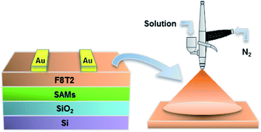
We herein present the results from our study of spray-coated poly[(9,9-dioctylfluorenyl-2,7-diyl)-co-bithiophene] (F8T2) semiconducting polymer films for organic thin film transistor (OTFT) applications. Optimized spray-coating parameters were performed for deposition of F8T2 layer on Si/SiO2 substrate treated with self-assembled monolayers (SAMs) of organosilane compounds. OTFTs fabricated from general spin-coating on the same substrate were also tested to evaluate the quality of active F8T2 layer. Comparable OTFT electrical performances can be obtained for both cases even through the spray-coated devices have high surface roughness and low overall homogeneity. The spray-coated F8T2 OTFTs on the SAMs-modified substrate exhibit a maximum hole mobility of ∼7.8 × 10⁻³ cm2 V−1 s−1 and ON/OFF ratios of over 105. These results confirm that the spray-coating method is a powerful tool in production of reliable and reproducible OTFTs, displaying a great potential for other solution-processable organic (opto-)electronics devices.


Introduction

Organic thin film transistors (OTFTs) have attracted significant attention from both industry and academia due to their advantageous features of low fabrication cost, ease of solution processing, increasing charge mobilities, structural flexibility and integrated compatibility.1–13 Many efforts towards the enhanced electrical performance and simplicity of OTFTs fabrication have been made. Up to now, the solution-processed OTFTs perform well due to the continuing improvements in charge mobility to values as high as amorphous silicon (a-Si) thin film transistors and are potentially promising for use in plastic electronics.1–13 According to the processing procedures, direct coating and transfer printing are the two main categories that in particular can be used to offer versatile strategies for solution-processed organic semiconductors in fabrication of OTFTs.13 Transfer patterning needs to pattern the active materials on a specific target substrate via a transfer medium; however, the associated contamination and contact force between the transfer medium and contact target can determine the success of deposition during the consequent transfer process. Therefore, direct coating is quite appropriate for high-throughput and mass-production of OTFTs fabrication. Spin-coating of solution-processed materials is typically preferred in current laboratory fabrications and an inherently large amount of material is wasted, whereas inkjet-printing, screen blading and spray-printing can be utilized as cost-effective and less-complex direct coating methods and are logically compatible with large scale manufacturing.13

Among these, spray-coating is the subject of our interest since it has come up with advantages of being able to coat the organic/polymer thin film for a large number of potential applications ranging from transistors, photovoltaic cells, electrochemical devices and chemical/biological sensors to biomedical applications.14–25 Spray-coating in general compromises N2- or air-pressurized atomization of a solution mixture through the nozzle, tiny droplet coalesce and flight in the vertical direction, solvent evaporation, droplet spreading and drying, and adhesion of solid parts attached on the substrates to form the thin film layer. Spray-coating needs the related processing parameters to be manipulated such as solution concentration, solvent used, spraying distance between nozzle and substrate, carrier gas pressure and substrate types and annealing temperature, etc. Since the spray-deposited OTFTs are not fully understood and the results are now still inconclusive, the aim of this work is to gain more significant insight into the properties of spray-on semiconducting layer. All these issues can be taken into consideration for optimizing the OTFTs characteristics.

Chan et al. have investigated poly(3-hexylthiophene) (P3HT)-based OTFTs fabricated by airbrush deposition technique. Here, we report a detailed study of optimization of spraying parameters on the quality of the resulting conjugated polymer semiconductors coating. The spraying process was performed under the ambient conditions since commercially available poly[(9,9-dioctylfluorenyl-2,7-diyl)-co-bithiophene] (F8T2) semiconducting polymer is formulated for good performance as well as high stability against environmental conditions. The use of self-assembled monolayers (SAMs) of organosilanes was introduced between spray-coated F8T2/SiO2 interface to control the interfacial properties. The structural effects were determined using polarizing optical microscope and UV-Vis absorption spectroscopy. Statistical analysis on the OTFTs characteristics is performed as guideline for influencing processing parameters. Semiconducting F8T2 films using spray-coating process exhibited a maximum hole mobility of ∼7.8 × 10⁻³ cm2 V−1 s−1 and ON/OFF ratios of over 105 comparable to spin-coated device and can be used in the large scale fabrication of solution-processable OTFTs.

Experimental

Fabrication of OTFTs

The device fabrication process was performed on Si wafers with 300 nm thermally grown oxide as gate dielectric and substrates were first cleaned by ultrasonication in acetone for 15 min and isopropanol for 15 min and then dried under nitrogen flow. The Si wafer (2 × 2 cm2) treated with SAMs of phenyltrichlorosilane (PTS) or octyltrichlorosilane (OTS) was used as bottom substrate. The semiconducting F8T2 (from American Dye Source, Inc. (Canada); Mw ∼ 38[thin space (1/6-em)]000 g mol−1) solution with approximately 4 mg ml−1 in dichlorobenzene (stirred overnight and filtered through PTFE syringe filter before use) was loaded into the commercially available pistol-type airbrush with a nozzle size of 0.3 mm and sprayed onto the substrate using a N2 pressure of 15 psi. The nozzle-to-substrate surface distance and deposited time were varied to control the quality and thickness of F8T2 layer. After spraying, the F8T2 film was heat treated at ∼80 °C for 30 min. 50 nm thick source and drain Au electrodes were deposited by thermal evaporation on the F8T2 semiconducting layer through the shallow mask.

Characterization

Polarizing optical microscopy images was acquired using Carl Zeiss Axiophot microscope equipped with AxioCam ERc5S camera. UV-Vis absorption spectra were recorded on a BioTek Synergy H1 spectroscopy. All the electrical measurements were conducted at room temperature with a semiconducting characterization system (Keithley 4200-SCS) on a manual probe station in N2-filled glove box. Field effect mobility (μ) was obtained in the saturated region of transistor operation by using the following equation, Id = (W/2L)Ciμ(VgVth)2, where W/L is the channel width/length, Ci is the gate dielectric capacitance per unit area, and Vg and Vth are the gate voltage and threshold voltage, respectively. The μ data here came from the devices with 40 μm channel length and 1000 um channel width. Average data were calculated from analysis of at least 15 devices.

Results and discussion

Spraying deposition technique involves an inexpensive, mass and easy scalable manufacturing process. The schematic diagram of the experimental setup to deposit F8T2 thin films via spray-coating is depicted in Fig. 1. Spray nozzle was set perpendicular towards the sample. The manipulation of spraying kinetics is feasible for film-forming properties. The spraying parameters such as N2 pressure, the distance between the nozzle and substrate surface, spray time and spray temperatures can be optimized to obtain good F8T2 thin film. The nozzle-to-substrate surface distance is typically maintained at 15–17 cm. A further reduction in this distance can result in a wetting and non-uniformed film. The droplets completely dried before colliding with the substrate result in poor adhesion and fail deposition. Therefore, forcing the F8T2 solution from sufficiently high N2 stream results in the formation of fine droplets that immediately dry after hitting the substrate surface. Morphological properties of the spray-coated F8T2 thin films were investigated by polarized microscope, as shown in Fig. 2. All the devices prepared from different surface conditions exhibit nearly similar F8T2 droplet domain size (20–50 μm) even through there are large differences in the mobilities between the devices with SAMs treatment or those without it as discussed later. Continuous F8T2 thin film was obtained with a layer thickness of 75 ± 25 nm (controlled by deposition time; typically ∼60 s). The substrate surface properties clearly have an impact on spreading of droplets. A superposition/merging of the droplets with disk-like structure deformation and large-scale surface roughness are generally visible in the topography of the deposited film; however, good F8T2 film coverage on the PTS-treated surface (Fig. 2(c)) can potentially provide good consistencies of electrical properties even in a large area deposition.
image file: c4ra03726j-f1.tif
Fig. 1 Schematic illustration of the spray coating system for OTFTs fabrication.

image file: c4ra03726j-f2.tif
Fig. 2 Polarizing microscope image of the F8T2 spray-coated thin film prepared on (a) bare SiO2 and (b) OTS- and (c) PTS-modified substrate.

The UV-Vis absorption spectra of spray-coated and spin-coated F8T2 thin films on SAMs/quartz substrates were measured and are shown in Fig. 3. Both F8T2 thin films exhibit a broad absorption range from 350 to 550 nm and similar position in absorption spectra with the maximum at 460 nm and vibronic band at 485 nm. Slightly blue-shifted absorption edge and decease in relative intensity for higher wavelength peak based on the spray-coated F8T2 film may be due to a reduced molecular interaction and disordered chain alignment. Note that the spray-coated film still have strong electronic perturbation due to the π–π stacking of F8T2 chain.26


image file: c4ra03726j-f3.tif
Fig. 3 UV-Vis absorption spectra of spray-coated and spin-coated thin film.

Top-contact bottom-gate (TCBG) OTFTs were fabricated in which source and drain electrode was vacuum-deposited on top of semiconducting layer, as shown in Fig. 1. The electrical characteristics of the F8T2 OTFTs were examined by output (IdVd) and transfer (IdVg) measurement. The organic buffer layer on the SiO2 surface can play a critical role on the OTFTs performance. Fig. 4(a) and (b) depict the transfer and output characteristics of spray-coated F8T2 OTFTs based on OTS- and PTS-functionalized substrates, respectively (for the case of bare SiO2/Si substrates, see Fig. S1 of ESI). The output characteristics are measured with a gate bias that varies from 0 to −60 V in steps of −10 V and exhibit well-defined linear and saturated regimes with a typical p-channel operation mode. The transfer curves in Fig. 4 also show that the spray-coated F8T2 devices have low gate OFF currents to be below 10−11 A. The hole mobility (μh) can be deduced to be based on respective transfer curves swept in the Vg range of 0 V to −60 V at a Vd of −60 V. The Vth is determined from a linear extrapolation of Id1/2 versus Vg. Table 1 summarizes the OTFTs performance data (including μh, ON/OFF current ratio (ION/IOFF) and Vth) of the devices prepared on the non- or OTS- or PTS-modified SiO2/Si substrates. The charge modulation of the F8T2 current channel is influenced by the attached interactions between F8T2 droplet and underlying layers and is reflected on the μh. Notably, OTFTs on SAMs-modified surface exhibit a steep parabolic slope in transfer characteristics and well-defined saturated region in output characteristics. Among these, the OTFTs prepared on OTS substrates have a highest μh (as high as ∼7.8 × 10⁻³ cm2 V−1 s−1), and SAMs-modified substrates provide one order of magnitude higher μh compared with the bare SiO2/Si substrate while ION/IOFF is also improved substantially after SAMs treatment and has a similar increasing trend with the μh results. This is mainly due to the reduced charge trapping defect at the spray-coated F8T2 semiconductor/SAMs-modified dielectric interface. Passivation of SiO2 surface by SAMs and the long alkane chain ends in OTS/phenyl rings in PTS allowed to interact with stacking of aromatic rings in F8T2 can effectively enhance the charge mobility. When comparing the μh in different SAMs surfaces, it can be observed that the OTFTs characteristics fabricated by spray-coating on PTS-modified substrate are consistently superior to those deposited by other conditions. Specifically, the collected μh prepared from OTS-modified substrate varies in a relatively broad range as compared to PTS-modified substrate mainly attributed to the incomplete coverage and inhomogeneity of F8T2 layer caused by the spraying process (see Fig. 2(b) & (c)). Presumably good wettability and spreading of F8T2 droplet on the PTS-modified surface increase the contact area between the F8T2 and substrate, favoring the continuous attachment. Surface treatment with PTS results in more tightly distributed μh value of F8T2-based OTFTs. However, the morphologies of spray-coated F8T2 thin film under different SAMs surfaces were also investigated by AFM topographies (Fig. S2 of ESI). In a microscopic level, small aggregated domains appear in the F8T2 thin film layer prepared from PTS-modified substrate, suggesting the reduced interchain charge transport properties. Probably good F8T2 chain connection within the droplet causes that the average mobility of F8T2 device from OTS-modified surface is slightly higher than from PTS-modified surface. Besides, all Vth data exhibit no significant change perhaps originated from the large charge injection barrier from the work function of Au source/drain electrodes into the HOMO level of F8T2 semiconducting layer or rough top-contact interface of Au/F8T2 rather than from F8T2/dielectric interface trapping. Therefore, the results suggest that the spray-coating method indeed can be used to fabricate the high degree device-to-device performance uniformity.


image file: c4ra03726j-f4.tif
Fig. 4 Transfer curves (upper) and output curves (lower), measured for the spray-coated F8T2 OTFTs on (a) OTS- and (b) PTS-modified substrate.
Table 1 Summary of F8T2 OTFTs performance fabricated from spray-coating and spin-coating method
  μh (cm2 V−1 s−1) ION/IOFF (−) Vth (V)
a Fabricated from spray-coating method.
Bare SiO2a (2.3 ± 1.6) × 10−4 (7 ± 2) × 104 −24.8 ± 1.7
OTSa (5.2 ± 1.4) × 10−3 (4 ± 1) × 104 −24.1 ± 2.4
PTSa (2.0 ± 0.3) × 10−3 (6 ± 2) × 105 −23.1 ± 3.7
Spin-coating (2.2 ± 0.4) × 10−3 (8 ± 1) × 105 −28.8 ± 1.7


In parallel with the spray-deposited OTFTs, spin-coated F8T2 OTFTs were also tested for comparison (Fig. S3 of ESI). It is noted that the Id of spray-coated OTFTs has almost similar order of magnitude with spin-coated ones and comparable μh results (>10−3 cm2 V−1 s−1) can also be obtained for both cases.26,27 Therefore, suitable drying time by controlling the nozzle-to-substrate surface distance may introduce the F8T2 droplets reorganization although the presence of the surface boundary and microscale film roughness during the spray-coating process may limit the current transport channel. While the film uniformity and roughness are subject to more variability, the resulting devices prepared from spray-coating still show remarkable tolerance to these differences. The spray-coating technique can not only be used to deposit the polymer semiconducting layer in the solid substrates, it can also be used to obtain all layers in OTFTs (electrode and dielectric layer) patterned in terms of the flexible substrates. An automatic spray-coating system can be implanted for further controlling the processing parameters. This subject is now under investigation and will be reported elsewhere.

Conclusions

In conclusion, we have herein described a facile spray-coating process for fabricating OTFTs devices, thereby allowing the simple manufacturing on cost-efficient, large-area and high-performance organic electronic devices. Spray-coated F8T2 OTFTs show the comparable transistor properties with spin-coated counterpart despite the high surface roughness and less organized film structures. These spray-coated semiconducting films provide an easy and fast approach to further develop the optimized framework for the solution-processable organic device such as memories, sensors, solar cells and active-matrix flat-panel display devices.

Acknowledgements

The authors gratefully acknowledge the funding from the Ministry of Science and Technology of Taiwan.

References

  1. J. Mei, Y. Diao, A. L. Appleton, L. Fang and Z. Bao, J. Am. Chem. Soc., 2013, 135, 6724 CrossRef CAS PubMed.
  2. C. B. Nielsen, M. Turbiez and I. McCulloch, Adv. Mater., 2013, 25, 1859 CrossRef CAS PubMed.
  3. C. Wang, H. Dong, W. Hu, Y. Liu and D. Zhu, Chem. Rev., 2012, 112, 2208 CrossRef CAS PubMed.
  4. Y. Wen, Y. Liu, Y. Guo, G. Yu and W. Hu, Chem. Rev., 2011, 111, 3358 CrossRef CAS PubMed.
  5. J. Zaumseil and H. Sirringhaus, Chem. Rev., 2007, 107, 1296 CrossRef CAS PubMed.
  6. H. Klauk, Chem. Soc. Rev., 2010, 39, 2643 RSC.
  7. S. Holliday, J. E. Donaghey and I. McCulloch, Chem. Mater., 2014, 26, 647 CrossRef CAS.
  8. J. D. Yuen and F. Wudl, Energy Environ. Sci., 2013, 6, 392 CAS.
  9. Q. Meng, H. Dong, W. Hu and D. Zhu, J. Mater. Chem., 2011, 21, 11708 RSC.
  10. R. P. Ortiz, A. Facchetti and T. J. Marks, Chem. Rev., 2010, 110, 205 CrossRef CAS PubMed.
  11. J. Sun, B. Zhang and H. E. Katz, Adv. Funct. Mater., 2011, 21, 29 CrossRef CAS.
  12. Z. Bao and J. Locklin, Organic Field-Effect Transistors, CRC Press, Boca Raton, FL, 2007 Search PubMed.
  13. B. Kang, W. H. Lee and K. Cho, ACS Appl. Mater. Interface, 2013, 5, 2302 CrossRef CAS PubMed.
  14. H.-Y. Park, H. Yang, S.-K. Choi and S.-Y. Jang, ACS Appl. Mater. Interface, 2012, 4, 214 CrossRef CAS PubMed.
  15. N. A. Azarova, J. W. Owen, C. A. McLellan, M. A. Grimminger, E. K. Chapman, J. E. Anthony and O. D. Jurchescu, Org. Electron., 2010, 11, 1960 CrossRef CAS PubMed.
  16. C. K. Chan, L. J. Richter, B. Dinardo, C. Jaye, B. R. Conrad, H. W. Ro, D. S. Germack, D. A. Fischer, D. M. DeLongchamp and D. J. Gundlach, Appl. Phys. Lett., 2010, 96, 133304 CrossRef PubMed.
  17. X. Yu, N. Zhou, S. Han, H. Lin, D. B. Buchholz, J. Yu, R. P. H. Chang, T. J. Marks and A. Faccetti, J. Mater. Chem. C, 2013, 1, 6532 RSC.
  18. D. Khim, K.-J. Baeg, B.-K. Yu, S.-J. Kang, M. Kang, Z. Chen, A. Facchetti, D.-Y. Kim and Y.-Y. Noh, J. Mater. Chem. C, 2013, 1, 1500 RSC.
  19. A. M. Munzer, M. Heimgreiter, K. Melzer, A. Weise, B. Fabel, A. Abdellah, P. Lugli and G. Scarpa, J. Mater. Chem. B, 2013, 1, 3797 RSC.
  20. H.-Y. Park, J.-S. Jin, S. Yim, S.-H. Oh, P.-H. Kang, S.-K. Choi and S.-Y. Jang, Phys. Chem. Chem. Phys., 2013, 15, 3718 RSC.
  21. S. Thiemann, S. J. Sachnov, M. Gruber, F. Gannott, S. Spallek, M. Schweiger, J. Kruckel, J. Kaschta, E. Spiecker, P. Wasserscheid and J. Zaumseil, J. Mater. Chem. C, 2014, 2, 2423 RSC.
  22. A. Abdellah, B. Fabel, P. Lugli and G. Scarpa, Org. Electron., 2010, 11, 1031 CrossRef CAS PubMed.
  23. C. M. Amb, A. L. Dryer and J. R. Reynolds, Chem. Mater., 2011, 23, 397 CrossRef CAS.
  24. F. C. Krebs, Sol. Energy Mater. Sol. Cells, 2009, 93, 394 CrossRef CAS PubMed.
  25. M.-C. Chen, H.-F. Liang, Y.-L. Chiu, Y. Chang, H.-J. Wei and H.-W. Sung, J. Controlled Release, 2005, 108, 178 CrossRef CAS PubMed.
  26. A. Salleo, M. L. Chabinyc, M. S. Yang and R. A. Street, Appl. Phys. Lett., 2002, 81, 4383 CrossRef CAS PubMed.
  27. E. Lim, B.-J. Jung, J. Lee, H.-K. Shim, J.-I. Lee, Y. S. Yang and L.-M. Do, Macromolecules, 2005, 38, 4531 CrossRef CAS.

Footnote

Electronic supplementary information (ESI) available. See DOI: 10.1039/c4ra03726j

This journal is © The Royal Society of Chemistry 2014
Click here to see how this site uses Cookies. View our privacy policy here.