DOI:
10.1039/C4RA03604B
(Paper)
RSC Adv., 2014,
4, 28409-28416
Highly robust SiCOH/mesoporous SiO2 ultralow dielectric films with heterostructures†
Received
20th April 2014
, Accepted 13th June 2014
First published on 17th June 2014
Abstract
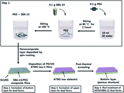
We report here a new dual-coating method for the deposition of SiCOH (elementally descriptive but not representing the stoichiometry) ATMS (allyltrimethylsilane) low-k films on mesoporous SiO2 (SBA-15)/PEG (polyethylene glycol) composite films to improve the dielectric constant and mechanical properties of SiCOH/SBA-15 dual forms. The deposition was achieved via a two-step process: (i) pre-treatment, where SBA-15 was mixed with a dispersion of PEG in DI water, and SBA-15/PEG composite films were formed by spin-coating; and (ii) post-treatment, involving the deposition of SiCOH films on SBA-15s functionalized with PEGs and post-thermal annealing. In comparison with SiCOH-only films, SiCOH/SBA-15 dual forms exhibited a 20% reduction in the dielectric constant without a significant loss of mechanical properties after post-thermal annealing. SEM, TEM, XRD, BET, FT-IR, EP, and XPS results show that the enhanced electrical properties can be attributed to mesoporous SiO2 and additional porosity gained through the removal of PEG and CxHy (thermally labile phases in SiCOH films) after post-thermal annealing. In the SiCOH/SBA-15 dual forms, the SBA-15 layer is expected to function as a soft layer which acts as a buffer layer to prevent the rapid decay of the modulus and hardness.
Introductions
Ultra low dielectric constant (k) interlayers (k < 2.2) are required to reduce the resistance–capacitance (RC) time delay, cross talk, and power dissipation in new-generation nanometer-sized electronics.1–5 The inclusion of air (k ∼ 1.0) in interconnected structures6,7 and the incorporation of nanopores into polymers8–10 are attractive approaches to reducing the dielectric constants of materials. The preparation of nanoporous low-k poly(silsesquioxane)s11–14 and polyimides15–19 from copolymers with thermally labile block or graft chains has been reported. It seems that the potential difficulties with many polyimides are borderline thermal stability, higher-than-desirable dielectric constants, the occurrence of anisotropic electrical and mechanical properties, significant water uptake, lower than desirable Tg values, and adhesion problems (both self-adhesion and adhesion to back end-of-line materials). Thus, these materials are questionable candidates as low-k replacement for oxides despite their common usage in the microelectronic industry, particularly in packaging areas.15–19
Siloxane polymers are potential candidates for interlayer dielectric applications because they have good thermal and mechanical stability, and have the lowest dielectric constant among the low-k materials.20–27 It is possible to obtain ultralow-k materials (k < 2.2) by introducing nanopores into SiCOH films.28–32 However, the mechanical properties of the films tend to degrade if the dielectric constant is reduced by increasing the porosity of the films. This leads to films that crack after curing or when exposed to mechanically demanding processing steps like chemical mechanical polishing (CMP), wire-bonding, chip dicing, etc. Because mechanical properties are intrinsic to a given material, the search for novel fracture-resistant dielectric insulators, particularly at high levels of porosity, has become the new low-k materials challenge.1,33–37,48
At present, the fabrication of a low dielectric material relies entirely on a single fabrication method, namely, direct growth by plasma-enhanced chemical vapor deposition (PECVD). This allows the preparation of a low-k (dielectric constant ∼2.2) material by introducing a porogen (pore generator) precursor in SiCOH films.1 However, due to the innate poor mechanical properties of pores, it is very difficult to achieve dielectric constants lower than 2.4 while maintaining a high modulus (>4 GPa) and hardness (>0.8 GPa).1,52,53
In this study, we report a new method for fabricating an ultralow dielectric material by adding an allytrimethylsilane (ATMS) SiCOH capping layer onto SBA-15 (mesoporous SiO2)/PEG composite films. The reduction in the dielectric constant of the dual SiCOH/SBA-15 forms is based on the direct removal of aliphatic chains (CxHy) and PEGs upon applying a post-thermal annealing. The whole procedure takes place as a facile process involving the formation of SBA-15/PEG composite films by spin-coating and subsequent preparation of the ATMS SiCOH layer by PECVD. This strategy leads to a reduction in the dielectric constant without a significant degradation of mechanical properties, unlike only PECVD or spin-coating treatments. The modulus enhancement mechanism in the SiCOH/SBA-15 dual forms can be considered on the basis of Koehler's theory.42–44 The hard material (SiCOH)/soft material (SBA-15, PEG)/hard material (Si substrate) sandwich structure also affects the modulus and hardness of the multilayer film.42,43 In this case, a soft material prevents any cracks generated in hard material layers from propagating across layers.42–44 For the SiCOH/SBA-15 dual forms, the SBA-15 layer is expected to function as a soft layer. Combined ATMS precursor and SBA-15 dual forms exhibited dielectric constants as low as 2.0, a modulus of up to 4.3 GPa, and a hardness of 0.9 GPa. These are excellent results for SiCOH low-k films.33–37 This suggests a new approach for improving the preparation of ultralow dielectric films for use in electronic devices.
Experimental
Preparation of mesoporous SiO2 (SBA-15)
The triblock copolymer P123 ((PEO)20(PPO)70(PEO)20, Molecular weight = 5800, Sigma-Aldrich) was dissolved in 2 M aqueous solution of hydrochloric acid at 38 °C. TEOS was added and vigorously stirred for 6 min. After aging at 38 °C for 24 h, the resulting solution was further heated at 100 °C for 24 h. The mixture was filtered and washed with 10 wt% aqueous HCl solution in ethanol to remove P123. SBA-15 was finally obtained after calcination at 550 °C in air. Ethanol (99.9% pure) were purchased from Merck. All chemicals used without purification or treatment, and deionized water (18 MΩ cm) purified by an ultrapure water system (Milli-Q, Millipore) was used in all experiments. Scheme 1 outlines the preparation procedure, which includes random orientation by using the spin-coating method, to form the porous structures (steps 1 to 2). Use of amphiphilic triblock copolymers (P123) to direct the organization of polymerizing silica species has resulted in the preparation of well-ordered hexagonal mesoporous silica structures (SBA-15) with uniform pore sizes up to approximately 10 nm (Fig. 2).38,39
 |
| Scheme 1 Fabrication of SBA-15/PEG composite films by the spin-coating method, and their post-deposition of SiCOH (ATMS) low-k films onto the SBA-15/PEGs.39,48 | |
Preparation of SiCOH/(SBA-15/PEG) dual forms
Scheme 1 illustrates the procedure employed for fabricating SBA-15/PEG films, including the post-treatment of SiCOH films. An SBA-15 dispersion was prepared with PEG (step 1): SBA-15 was dispersed in DI water and the suspension was added to PEG (polyethylene glycol); the mixture was then heated at 80 °C for 1 h. The SBA-15/PEG suspension was spin-coated onto an Si wafer substrate to form the bottom layer (step 2). PEG concentrations of 2 and 3 wt% were mixed with the SBA-15 aqueous dispersion. SBA-15/PEG composite films were positioned between the shower head PECVD distributor and the heated plate such that plasma irradiation and precursor injection were mutually parallel. We used ATMS as a passivation molecule to maintain the stability of the dual structure because ATMS PECVD films have a low dielectric constant and are thermally and mechanically stable (step 3).48 When post-thermal annealing was applied to ATMS/(SBA-15/PEG) dual forms, the thermally labile phases such as PEG and CxHy (aliphatic chain) were removed. As-prepared samples were annealed in ambient Ar for 2 h using a tube furnace equipped with a vacuum system. The tube furnace temperatures were calibrated using a thermocouple and the post-thermal annealing temperature was fixed at 420 °C. In our experiments, the thermal treatment was not applied until the vacuum reached <60 mTorr. After post-thermal annealing, SBA-15 maintained a porous matrix in the absence of a PEG binder (step 4).
Surface morphology measurements
The morphological changes of the SBA-15 and SBA-15/PEG composites after SiCOH deposition were characterized using SEM (FE-SEM, FEI company Magellan400) and TEM (FE-TEM, JEM-2100F/JEOL). SEM images were obtained by collecting secondary electrons produced by bombarding the sample under an acceleration voltage of between 0.8 and 1 kV. TEM samples were prepared as previously reported,39 and the nanostructures of SBA-15 were analyzed using a TEM in bright-field mode at 200 kV.
Crystalline, chemical structure, surface area, and pore size measurements
XRD data XRD data for SBA-15 samples was collected on a small-angle X-ray diffractometer (D/MAX-2500, RIGAKU) with a transmission method, 18 kW high power generator (using fine focus), automatic 3rd slit, and an image plate system. For as-made samples, XRD peaks were observed in the interval of d-spacings up to 0.1 Å, which comprised 40 symmetrically independent reflections. The chemical bonding and composition of the films was investigated using a Fourier transform (FT) IR spectrometer (MIDAC, USA) and X-ray photoemission spectroscope (XPS, Thermo VG Scientific Sigma Probe). Baseline-corrected FT-IR spectra were obtained for samples over a range of 400–4000 cm−1 at a resolution of 4 cm−1 averaged over 64 scans, performed in transmission mode. Peak area calculations were performed using OMNIC software. Atomic composition and peak deconvolution of the XPS data was carried out with Thermo Advantage (Thermo Fisher Scientific) software. High-resolution spectra were acquired using a microfocused monochromator X-ray source (1486.6 eV). In order to remove carbon contamination from the sample surface, 10 s of sputter cleaning with 3 keV Ar ions was carried out before the analysis. XPS survey scans were performed with an operating pressure of ∼1 × 10⁻⁹ Torr. Monochromatic X-rays (1486.6 eV) with a 400 μm beam diameter were used. An electron flood gun was used for charge neutralization. Photoelectrons were collected at a 55° emission angle. A hemispherical analyzer collected photoemission electrons with a pass energy of 150 V for survey scans. The 1 s level in carbon (284 eV) and oxygen (532 eV) and the 2 s level in silicon (102 eV) were analyzed. Energy resolution was 0.47 eV FWHM. Nitrogen adsorption–desorption isotherms were measured using a Micromeritics ASAP 2010 system. The data was calculated using the BdB (Broekhoff and de Boer) model. The pore size distribution curve was obtained from analysis of the adsorption branch of the isotherm. Toluene adsorption–desorption isotherm measurement protocol was as follows: samples were heated to 150 °C for 5 min on a separate hot plate before porosimetry measurements. Wafers were placed in a vacuum chamber, then porosimetry cycled with toluene as the solvent. Spectroscopic ellipsometric porosimetry measurements were evaluated automatically. Samples were located on an adaptation plate on the robot loader arm of the PS-2000 ellipsometric porosimeter system.
Dielectric and electrical properties measurements
The dielectric constant was measured using capacitance–voltage (C–V) measurements of a metal/insulator/semiconductor (MIS) structure (Hg/0.3–3 μm thick dielectric film/Si) with an Hg electrode area of 4.5 × 10⁻³ cm2 at 1 MHz. Measurements of the capacitance were carried out using a HP 4284A impedance analyzer. The dielectric constant was calculated using the following equation: |
 | (1) |
The final film thickness was measured using Alpha-step IQ (Surface Profiler, KLA Tencor).
Mechanical property measurements
The mechanical properties of the films were measured at room temperature using a Nano Indentation System (MTS, Nano Indenter XO) based on ISO-14577.17 Nine points on each sample were assayed by continuous stiffness measurements (CSM), and the average and standard deviation were calculated. The first 10% of the film thickness was taken as the indentation depth range to determine the Young's modulus and the hardness, and the values were compared with corresponding results from other samples. The Poisson ratio of the SiCOH films was 0.25, as calculated from the Young's modulus.
Results and discussion
Scheme 1 outlines the preparation procedure of SBA-15 and PEG nanocomposite with random orientations using spin-coating to yield porous structures (steps 1–4). The use of amphiphilic triblock copolymers (P123) to direct the organization of polymerized silica species results in the preparation of well-ordered hexagonal mesoporous silica structures (SBA-15) with uniform pore sizes up to approximately 10 nm (Fig. 1).38,39 First, SBA-15 was dispersed in an aqueous PEG solution and the mixture was heated at 80 °C for 1 h. In this step, PEG attached to functional groups such as the Si–O network and hydroxyl at the surface of SBA-15 by means of thermal decomposition. PEG-hybridized SBA-15 was fabricated during the chemical reaction without the use of any additional agents. The resulting water suspension of SBA-15/PEG was dropped on the substrate (Si wafer) with spin-coating to form the bottom layer (step 2). SBA-15/PEG composite films were then positioned between the PECVD shower head (i.e. the distributor of precursors) and a heated plate such that the plasma irradiation and the precursor injection were mutually parallel. The passivation species maintains stability of the dual structure; we used ATMS as SiCOH films of the material have a low dielectric constant and good thermal and mechanical properties (step 3).48 When post-thermal annealing was applied to the ATMS/(SBA-15/PEG) dual forms, thermally labile phases such as PEG and CxHy (aliphatic chain) were removed. After annealing, SBA-15 maintained the porous matrix in the absence of a PEG binder (step 4). The deposition condition of ATMS and the ratio of PEG/SBA-15 were varied to achieve low dielectric constant dual forms with excellent mechanical properties.48
 |
| Fig. 1 Powder small angle XRD patterns of annealed mesoporous silica (SBA-15) prepared using the amphiphilic triblock copolymer P123 as structure-directing species. | |
The small angle XRD pattern for calcined mesoporous silica (SBA-15) prepared with P123 shows three well-resolved peaks (Fig. 1) that are indexable as (100), (110), and (200) reflections associated with p6mm hexagonal symmetry.38 Two additional weak peaks in the 2θ range of 2 to 3.5 correspond to the (300) and (220) scattering reflections, indicating that annealed SBA-15 has a high degree of hexagonal mesoscopic organization.45,46
After post-thermal annealing in Ar at 550 °C for 6 hours, the XRD pattern (Fig. 1) shows that the p6mm morphology was preserved, although the peaks appear at slightly larger 2θ values, with d(100) = 93.3 Å and a large unit-cell parameter (a0 = 110 Å).3 Five XRD peaks are still observed, confirming that hexagonal SBA-15 is thermally stable. A similarly high degree of mesoscopic order (three p6mm XRD peaks) was observed for hexagonal SBA-15 even after calcination at 550 °C.
SEM images (Fig. 2a and b) reveal that annealed SBA-15 samples consisted of comb and net-like domains with relatively uniform pore sizes of ∼10 nm. TEM images (Fig. 2c and d) of annealed SBA-15 show well-ordered hexagonal arrays of mesopores (1D channels) and further confirm that SBA-15 has a 2D p6mm hexagonal structure.45,46 From high-dark contrast in the TEM images of this sample (Fig. 2c and d), the distance between mesopores was estimated to be ∼10 nm, in agreement with that determined from the XRD data.
 |
| Fig. 2 SEM images of calcined mesoporous silica (SBA-15) showing the top and side view (a and b). The red circle in (a) indicates a hexagonal structure and nanopore (<10 nm). The yellow circles in (b) show side view of SBA-15, which have a net structure (pore size ∼10 nm). TEM images of mesoporous SiO2 (SBA-15) showing the top view (c) and the side view (d), respectively, having (c) a hexagonal basal plane with a well-ordered hexagonal array and (d) a highly ordered periodic structure consistent with a hexagonal close-packed arrangement of channels running parallel to the surface of the powder. | |
For detailed structure analysis, we measured the pore size distribution and surface area of SBA-15. As shown in Fig. 3, the SBA-15 produced in this study shows a mean pore size of 7.4 nm and a Brunauer–Emmett–Teller (BET) surface area of 802.6 m2 g−1, as calculated using the BdB (Broekhoff and de Boer) model.45 Three well-distinguished regions of the adsorption isotherm (Fig. 3) are evident: (i) monolayer–multilayer adsorption, (ii) capillary condensation, and (iii) multilayer adsorption on the outer surface of particles. In contrast to N2 adsorption results for MCM-41 mesoporous silica, which has pore sizes ∼4 nm, a clear type-H1 hysteresis loop was observed, and capillary condensation occurred at a higher relative pressure (P/P0 ∼ 0.7).45,46 The approximate pore size calculated using Barrett–Joyner–Halenda analysis was significantly smaller than the repeat distance determined by XRD. The Halsey equation was used for multilayer thickness because the latter includes the thickness of the pore wall.47 The pore wall thickness was estimated to be ∼5 nm (Fig. 2) for SBA-15 prepared with P123. The BET surface area and pore size in SBA-15 is consistent with other reports.38,39
 |
| Fig. 3 Nitrogen adsorption–desorption isotherm plots (a) and pore size distribution curves (b) for annealed mesoporous SiO2 (SBA-15) prepared using TEOS (tetraethylorthosilicate) as a silica source, ethanol as a solvent. | |
To understand the effect of the allyl functional moiety, deposition temperature, and post-thermal annealing on the dielectric constant of the ATMS film, FT-IR (Fig. 4) and XPS (Fig. 5) measurements of the ATMS dielectric films were carried out. The absorption peaks of Si–CH3 (800, 845, 1270 cm−1) and the Si–O peak (1030 cm−1) were observed in dielectric films deposited at 120 °C (Fig. 4a), and CHm (m = 1–3) stretching peaks, which indicate aliphatic chains, were detected at 2930 and 2970 cm−1 (Fig. 4b). With a high deposition temperature (210 °C), the Si–O cage-like peak at 1135 cm−1 appeared more strongly than for the film deposited at 120 °C (see the arrow in Fig. 4c).1,9,34 It has been reported that this cage-like structure can lead to a micro-porous film with a lower density.1,27 These FT-IR results suggest that thermal annealing treatment can lead to rearrangement of the amorphous covalent bonded network of the as-deposited films.1,26 This rearrangement contributes to the formation of nano-porosity within the films.
 |
| Fig. 4 FT-IR spectra of the ATMS dielectric films before and after annealing at 420 °C in the wavenumber range of (a) 600–1600 cm−1 and (b) 2700–4000 cm−1 for the 120 °C deposition films, and in the same range (c) and (d) for the 210 °C deposition films, respectively. | |
 |
| Fig. 5 XPS analysis of ATMS dielectric films deposited at 120 °C; (a and c) are Si2p spectra, and (b and d) are C1s spectra. (a and b) ATMS dielectric films before annealing. The peak shift and intensity change after annealing are represented in (c and d). The O2/ATMS ratio was 2.5 and the annealing temperature was 420 °C. | |
XPS of the dielectric films was carried out to further verify the chemical structure of ATMS films. Fig. 5 shows high resolution Si2p and C1s spectra of the ATMS dielectric films. Each spectral region was deconvoluted into individual peaks by assuming all peaks to be perfectly Gaussian with a FWHM (full width at half maximum) of 1.45. Before thermal annealing, the Si2p spectra were deconvoluted into five moieties:40 SiO4 (104.9 eV), SiO3 (103.7 eV), SiO2 (102.6 eV), SiO1 (101.7 eV), and SiO0 (100.6 eV) (Fig. 5a). The C1s spectra were deconvoluted into four moieties:40 CSin (283.5 eV), Si–CH3 (284.5 eV), CO1 (285.3 eV), and CO2 (286.3 eV) (Fig. 5b). From the area of the peaks, the majority of the C moiety was Si–CH3 at 284.5 eV, which is in good agreement with the FT-IR spectra (Fig. 4). After post-thermal annealing, the appearance of more SiOx (x = 2, 3, 4) implied that the oxygen content of the film had increased (Fig. 5c). Simultaneously, the decrease in the carbon content of the film after annealing is due to the removal of labile carbon groups (Fig. 5d).37,40,41 These trends are consistent with the results for deposition at 210 °C. Based on the FT-IR and XPS spectra, it was concluded that the formation of an Si–O cage-like structure was enhanced by the higher deposition temperature. The low energy oxygen plasma and the involvement of each monomer unit in multiple polymer chains can produce Si–O networks containing methyl and aliphatic chains.1,40 After thermal annealing, unstable carbon groups (CxHy, aliphatic groups) are removed and a three-dimensional Si–O matrix with uniform porosity is formed, arising from steric hindrance by the methyl groups.40
The porosity and average pore radius of ATMS dielectric films were 7.4% and 0.61 nm, respectively (Fig. 6). Pore Radius Distributions (PRDs) were desirably narrow and microporous, below 1.6 nm (Fig. 6b). In the ATMS system, the main pore size was 0.5–0.6 nm, of which the main portion was microporous rather than mesoporous. Ellipsometric porosimetry (EP) measures the change in optical properties and thickness of a material during an adsorption experiment. The pores in the layer are filled gradually by an adsorptive (solvent) material such as toluene. Changes in the optical properties are simultaneously detected using spectroscopic ellipsometry (an optical technique). Pore analysis was considered with the Dubinin-Radushkevich (DR) model and the modified Kelvin equation. The pore size distribution (PSD) was calculated from the refractive index and the volume adsorbed isotherm. The volume adsorbed isotherm was first calculated from the refractive index isotherm using the Lorentz–Lorenz equation.54
 |
| Fig. 6 Toluene adsorption–desorption isotherm plots (a) and pore size distributions (b and c) of ATMS dielectric films deposited at 210 °C. The ATMS ratio was 2.5 and the annealing temperature was 420 °C. | |
As shown in Fig. 7, the morphology of spin-coated SBA-15/PEG composite films was investigated using SEM. The SBA-15/PEG composite films were relatively uniform, and PEG filled the vacancies in the SBA-15 network. From high magnification SEM images (Fig. 7c and d), we found that PEG comprised the matrix of films prior to post-thermal annealing at 420 °C. Following annealing, the PEGs were removed and a porous structure was produced in the SBA-15/PEG composite films. Changes in the morphology of SBA-15 itself were not detected after thermal annealing since the main component of SBA-15 is SiO2, which is a thermally stable phase.
 |
| Fig. 7 (a and c) SEM images of the as-deposited SBA-15/PEG composite films and (b and d) annealed SBA-15/PEG composite films. A high-magnification SEM image shows the removal of PEG (yellow circle) (d). | |
We found that the PEG/SBA-15 ratio and spin coating speed in step 2 (Scheme 1) are important factors controlling the uniformity of the ATMS(SiCOH)/SBA-15 films. The higher the PEG/SBA-15 ratio, the greater the planarization of the SiCOH/SBA-15 dual forms. As the spin coating speed decreases, the vacancies of composite films are filled to a greater extent. Fig. 8 shows cross-sectional SEM images of SiCOH/SBA-15 composite films after post-thermal annealing at 420 °C. The roughness and uniformity were enhanced by spin coating at 700 rpm with a PEG/SBA-15 ratio of 2.
 |
| Fig. 8 Typical images of the ATMS/SBA-15 dielectric film (PEG/SBA-15 ratio of 2); (a and b) are cross-sectional SEM images, (c and d) are surficial SEM images showing the roughness of the ATMS/SBA-15 dielectric films. Yellow circles show film vacancies. The spin coating speed of (a and c) and (b and d) was 700 and 1000 rpm, respectively. | |
A Nano Indentation System was used to measure the mechanical properties, such as Young's modulus and hardness, of the ATMS SiCOH material and ATMS/SBA-15 composite films. Data is presented in Table 1. The ATMS low-k films deposited at 210 °C were highly robust, but the dielectric constant was relatively high.48 SBA-15 and SiCOH hybrid films produced in this work can reduce the dielectric constant (2.0) while compensating for the reduction in mechanical properties (Young's modulus ∼4.3 GPa, hardness ∼0.9 GPa). This mechanical enhancement in spite of the low dielectric constant can be considered on the basis of Koehler's theory.42–44 The sandwich structure of hard material (SiCOH)/soft material (SBA-15)/hard material (Si substrate) also affects the modulus and hardness of the multilayer film.42,43 In this case, a soft material prevents cracks that are generated in a hard material layer from propagating into other layers.42–44 For the SiCOH/SBA-15 dual forms, the SBA-15 layer is expected to function as a soft buffer layer that prevents the modulus and hardness from decaying quickly. The mechanical performance of dual forms is superior to that of other SiCOH materials (Table S1†).33–37,48–51 A deposition temperature of 120 °C led to a dielectric constant that was reduced to 1.8. We found that the mechanical properties of the film were strongly affected by the deposition temperature and post-thermal annealing (Table 1).48 In the middle of temperature (about 160–170 °C), the mechanical properties such as modulus and hardness of ATMS/SBA-15 composite films are relatively poor (E ∼ 3 GPa, H ∼ 0.5 GPa). In the high temperature over 210 °C, the growth rate of ATMS films was very low, and the dielectric constant was shifted to higher value (over 2.5). As shown in Fig. 5 and Table 1, the concentration of SiO2, SiO3, and SiO4 moieties increased after thermal annealing, and the SiO3 and SiO4 content in 210 °C deposited films was larger than for 120 °C deposited films.48 Because SiO2, SiO3, and SiO4 groups are more stable than SiO0 and SiO1, rearrangement of the Si–O network can enhance the modulus and hardness. Moreover, post-thermal curing can improve the film's mechanical properties by driving cross-linking reactions such as hydrolysis and condensation.15,34,40 SiCOH films as an upper layer can maintain robust mechanical performance, while porous SBA-15 films as a bottom layer can reduce the dielectric constant. A low dielectric constant and superb mechanical properties are essential factors in improving the reliability and performance of semiconductor devices.
Table 1 Dielectric constant and mechanical properties of SiCOH alone and SiCOH/SBA-15 composite films as a function of deposition temperature
Deposition temperature (°C) |
Materials |
Dielectric constant |
Modulus (GPa) |
Hardness (GPa) |
210 |
SiCOH |
2.5 |
6.9 |
1.35 |
SiCOH/SBA15 |
2.0 |
4.3 |
0.9 |
120 |
SiCOH |
2.5 |
2.1 |
0.35 |
SiCOH/SBA15 |
1.8 |
1.3 |
0.14 |
Conclusions
We demonstrated that the dual deposition of SiCOH low-k films onto SBA-15/PEG composite films can effectively enhance the dielectric constant and mechanical properties of the resulting SiCOH/SBA-15 dual forms without significant loss in modulus. Dual-structured films of SiCOH on SBA-15s were achieved using a facile process with two different deposition steps: (1) pre-treatment, by mixing PEG precursor with a dispersion of SBA-15s in DI water; and (2) post-treatment, with post-deposition of ATMS SiCOH low-k films onto SBA-15/PEG composites and post-thermal annealing. Both pre- and post-treatment with SBA-15s resulted in the formation of porous structures in the dual forms by thermal annealing. A small reduction in the modulus and hardness alongside an ultralow dielectric constant (∼2.0) occurred with SiCOH deposition and post-thermal annealing. This phenomenon can be explained by Koehler's theory, which addresses the combinatorial effects of a dual structure. SiCOH/SBA-15 composite films with dual forms of SiCOH and SBA-15 resulted in a significantly reduced dielectric constant (from 2.5 to 2.0), a modulus of 4.3 GPa, and a hardness of 0.9 GPa, as compared with other SiCOH films (see Table S1†). However, no additional enhancement in the mechanical properties of SiCOH/SBA-15 dual-forms was observed with low temperature deposition of the SiCOH upper layer during post-treatment. This implies that low deposition temperatures have no beneficial effect on the mechanical properties of SiCOH/SBA-15 dual forms, as indicated by a small modulus and poor hardness. This study is particularly relevant to the further development of ultralow dielectric films for use in optoelectronic devices such as ultra-large scale integrated (ULSI) circuits, displays, lenses, and solar cells.
Acknowledgements
This work was supported by KINC (KAIST Institute for the Nano Century)-KCC Corporation Joint Research Program (G01090227), the National Research Foundation of Korea (NRF) grant funded by the Ministry of Science, ICT and Future Planning, Korea (MSIP, NRF-2012R1A2A1A01003537) and Global Frontier Grant funded by center for Advanced Soft Electronics under the Global Frontier Research Program of the Ministry of Science, ICT and Future Planning, Korea (MSIP, Grant NRF-2012M3A6A5055744). Nanoindentor experiments were carried out at NNFC (National NanoFab Center) in KAIST.
Notes and references
- W. Volksen, R. D. Miller and G. Dubois, Chem Rev., 2010, 110, 56 CrossRef CAS PubMed.
- Y. Liu, M. Sun, C. M. Lew, J. Wang and Y. Yan, Adv. Funct. Mater., 2008, 18, 1732 CrossRef CAS.
- K. Landskron, B. D. Hatton, D. D. Perovic and G. A. Ozin, Science, 2003, 302, 266 CrossRef CAS PubMed.
- M. Ibn-Elhaj and M. Schadt, Nature, 2001, 410, 796 CrossRef CAS PubMed.
- J.-Q. Xi, J. K. Kim and E. F. Schubert, Nano Lett., 2005, 5, 1385 CrossRef CAS.
- L. S. Loo and K. K. Gleason, Electrochem. Solid-State Lett., 2001, 4, G81 CrossRef CAS PubMed.
- P. A. Kohl, D. M. Bhusarin and M. Wedlake, IEEE Electron Device Lett., 2000, 21, 557 CrossRef CAS.
- J. L. Hedrick, K. R. Carter, J. W. Labadie, R. D. Miller, W. Volksen, C. J. Hawker, D. Y. Yoon, T. P. Russell, J. E. McGrath and R. M. Briber, Adv. Polym. Sci., 1999, 141, 11 CrossRef.
- C. V. Nguyen, K. R. Carter, C. J. Hawker, J. L. Hedrick, R. L. Jaffe, R. D. Miller, J. F. Remenar, H. W. Rhee, R. M. Rice, M. F. Toney, M. Trollsas and D. Y. Yoon, Chem. Mater., 1999, 11, 3080 CrossRef CAS.
- A. M. Padovani, L. Rhodes, L. Riester, G. Lohman, B. Tsuie, J. Conner, S. A. Bistrup and P. A. Kohl, Electrochem. Solid-State Lett., 2001, 4, 25 CrossRef PubMed.
- R. Q. Su, T. E. Müller, J. Prochazka and J. A. Lercher, Adv. Mater., 2002, 14, 1369 CrossRef CAS.
- H. C. Kim, J. B. Wilds, C. R. Kreller, W. Volksen, P. J. Brock, V. Y. Lee, T. Magbitang, J. L. Hedrick, C. J. Hawker and R. D. Miller, Adv. Mater., 2002, 14, 1637 CrossRef CAS.
- C. C. Yang, P. T. Wu, W. C. Chen and H. L. Chen, Polymer, 2004, 45, 5691 CrossRef CAS PubMed.
- J. H. Lee, Y. Y. Lyu, M. S. Lee, J. H. Hahn, J. H. Rhee, S. K. Mah, J. H. Yim and S. Y. Kim, Macromol. Mater. Eng., 2004, 289, 164 CrossRef.
- R. J. McWhirter, Energy Res. Abstr., 1981, 6, 2627 Search PubMed.
- J. Gagliani and D. E. Supkis, Adv. Astronaut. Sci., 1979, 38, 193 CAS.
- B. Krause, G. H. Koops, N. F. A. van der Vegt, M. Wessling, M. Wubbenhorst and J. van Turnhout, Adv. Mater., 2002, 14, 1041 CrossRef CAS.
- R. A. Meyers, J. Polym. Sci., Polym. Chem., 1969, 7, 2757 CrossRef.
- L. Y. Jiang, C. M. Leu and K. H. Wei, Adv. Mater., 2002, 14, 426 CrossRef CAS.
- J. Cho, J. Hong, K. Char and F. Caruso, J. Am. Chem. Soc., 2006, 128, 9935 CrossRef CAS PubMed.
- Y. Hoshikawa, H. Yabe, A. Nomura, T. Yamaki, A. Shimojima and T. Okubo, Chem. Mater., 2010, 22, 12 CrossRef CAS.
- Z. Wang, A. Mitra, H. Wang, L. Huang and Y. Yan, Adv. Mater., 2001, 13, 1463 CrossRef CAS.
- A. M. Coclite, A. Milella, F. Palumbo, F. Fracassi and R. d'Agostino, Plasma Processes Polym., 2010, 7, 1022 CrossRef CAS.
- A. Milella, F. Palumbo, J. L. Delattre, F. Fracassi and R. d'Agostino, Plasma Processes Polym., 2007, 4, 425 CrossRef CAS.
- B. G. Prevo, Y. Hwang and O. D. Velev, Chem. Mater., 2005, 17, 3642 CrossRef CAS.
- A. Vincent, S. Babu, E. Brinley, A. Karakoti, S. Deshpande and S. Seal, J. Phys. Chem. C, 2007, 111, 8291 CAS.
- S. Chhajed, M. F. Schubert, J. K. Kim and E. F. Schubert, Appl. Phys. Lett., 2008, 93, 251108 CrossRef PubMed.
- K. Maex, M. R. Baklanov, D. Shamiryan, F. lacopi, S. H. Brongersma and Z. S. Yanovitskaya, J. Appl. Phys., 2003, 93, 8793 CrossRef CAS PubMed.
- H. S. Nalwa, Handbook of Low and High Dielectric Constant Materials and Their Applications, Academic, 1999 Search PubMed.
- S. J. Martin, J. P. Godschalx, M. E. Mills, E. O. Shaffer II and P. H. Townsend, Adv. Mater., 2000, 12, 1769 CrossRef CAS.
- G. Maier, Prog. Polym. Sci., 2001, 26, 3 CrossRef CAS.
- International Technology Roadmap for Semiconductors 2012, http://public.itrs.net/, accessed September 2012.
- V. Jousseaume, A. Zenasni, L. Favennec, G. Gerbaud, M. Bardet, J. P. Simon and A. Humbert, J. Electrochem. Soc., 2007, 154, G103 CrossRef CAS PubMed.
- D. D. Burkey and K. K. Gleason, J. Electrochem. Soc., 2004, 151, F105 CrossRef CAS PubMed.
- J. S. Rathore, L. V. Interrante and G. Dubois, Adv. Funct. Mater., 2008, 18, 4022 CrossRef CAS.
- G. Dubois, T. Magbitang, W. Volksen, E. Simonyi and R. D. Miller, Proc. IEEE Int. Interconnect Technol. Conf., 2005, 8, 226 Search PubMed.
- N. J. Trujillo, Q. Wu and K. K. Gleason, Adv. Funct. Mater., 2010, 20, 607 CrossRef CAS.
- D. Zhao, J. Feng, Q. Huo, N. Melosh, G. H. Fredrickson, B. F. Chmelka and G. D. Stucky, Science, 1998, 279, 548 CrossRef CAS.
- D. Zhao, J. Sun, Q. Li and G. D. Stucky, Chem. Mater., 2000, 12, 275 CrossRef CAS.
- J.-M. Park and S. W. Rhee, J. Electrochem. Soc., 2002, 149, F92 CrossRef CAS PubMed.
- S. K. Kwak, K. H. Jeong and S. W. Rhee, J. Electrochem. Soc., 2004, 151, F11 CrossRef CAS PubMed.
- E. Kusano, M. Kitagawa, H. Nanto and A. Kinbara, J. Vac. Sci. Technol., A, 1998, 16, 1272 CAS.
- X. Xiao and X. You, Appl. Surf. Sci., 2006, 253, 2958 CrossRef CAS PubMed.
- S. P. Baker and T. P. Weihs, Mater. Res. Soc. Symp. Proc., 1993, 308, 217 CrossRef CAS.
- J. S. Beck, J. C. Vartuli, W. J. Roth, M. E. Leonowicz, C. T. Kresge, K. D. Schmitt, C. T. W. Chu, D. H. Olson, E. W. Sheppard, S. B. McCullen, J. B. Higgins and J. L. Schlenker, J. Am. Chem. Soc., 1992, 114, 10834 CrossRef CAS.
- Q. Huo, D. I. Margolese and G. D. Stucky, Chem. Mater., 1996, 8, 1147 CrossRef CAS.
- R. Schmidt, E. W. Hansen, M. Stöcker, D. Akporiaye and O. H. Ellestad, J. Am. Chem. Soc., 1995, 117, 4049 CrossRef CAS.
- J.-M. Park, J. K. Choi, C. J. An, M. L. Jin, S. Kang, J. Yun, B.-S. Kong and H.-T. Jung, J. Mater. Chem. C, 2013, 1, 3414 RSC.
- T. Frot, W. Volksen, S. Purushothaman, R. L. Bruce, T. Magbitang, D. C. Miller, V. R. Deline and G. Dubois, Adv. Funct. Mater., 2012, 22, 3043 CrossRef CAS.
- S. Eslava, J. Urrutia, A. N. Busawon, M. R. Baklanov, F. Iacopi, S. Aldea, K. Maex, J. A. Martens and C. E. A. Kirschhock, J. Am. Chem. Soc., 2008, 130, 17528 CrossRef CAS PubMed.
- S. Eslava, F. Iacopi, M. R. Baklanov, C. E. A. Kirschhock, K. Maex and J. A. Martens, J. Am. Chem. Soc., 2007, 129, 9288 CrossRef CAS PubMed.
- M. R. Baklanov, P. S. Ho, E. Zschech, G. Dubois and W. Volksen, Advanced Interconnects for ULSI Technology, Wiley, 2012 Search PubMed.
- M. Baklanov, M. Green and K. Maex, Dielectric films for advanced microelectronics, Wiley, 2007 Search PubMed.
- F. Rouquerol, J. Rouquerol and K. S. W. Sing, Adsorption by powders and porous solids, Academic Press Inc., 1999 Search PubMed.
Footnote |
† Electronic supplementary information (ESI) available: Supplementary Fig. S1, Table S1–S3. See DOI: 10.1039/c4ra03604b |
|
This journal is © The Royal Society of Chemistry 2014 |
Click here to see how this site uses Cookies. View our privacy policy here.