Epitaxial growth of high-quality AlN films on metallic nickel substrates by pulsed laser deposition
Wenliang Wanga,
Weijia Yanga,
Zuolian Liua,
Yunhao Lina,
Shizhong Zhoua,
Huirong Qiana,
Haiyan Wanga,
Zhiting Lina and
Guoqiang Li*ab
aState Key Laboratory of Luminescent Materials and Devices, South China University of Technology, Guangzhou 510640, China. E-mail: msgli@scut.edu.cn; Tel: +86 20 87112957
bDepartment of Electronic Materials, School of Materials Science and Engineering, South China University of Technology, Guangzhou 510640, China
First published on 10th June 2014
Abstract
Single-crystalline AlN films have been grown on metallic nickel (Ni) substrates by pulsed laser deposition with an in-plane epitaxial relationship of AlN[11![[2 with combining macron]](https://www.rsc.org/images/entities/char_0032_0304.gif) 0]//Ni[1
0]//Ni[1![[1 with combining macron]](https://www.rsc.org/images/entities/char_0031_0304.gif) 0]. The as-grown AlN films reveal that a very smooth AlN film surface with a root-mean-square roughness of 1.0 nm has been obtained, and there is no interfacial layer existing between the AlN films and the Ni (111) substrates. Furthermore, with the increase in the growth temperature, the surface morphologies, crystalline qualities, and interfacial properties of as-grown AlN films gradually deteriorate. The as-grown about 300 nm-thick AlN films are almost fully relaxed only with an in-plane compressive strain of 0.67%. This work has potential in applications of AlN-based devices which require abrupt hetero-interfaces and flat films surfaces.
0]. The as-grown AlN films reveal that a very smooth AlN film surface with a root-mean-square roughness of 1.0 nm has been obtained, and there is no interfacial layer existing between the AlN films and the Ni (111) substrates. Furthermore, with the increase in the growth temperature, the surface morphologies, crystalline qualities, and interfacial properties of as-grown AlN films gradually deteriorate. The as-grown about 300 nm-thick AlN films are almost fully relaxed only with an in-plane compressive strain of 0.67%. This work has potential in applications of AlN-based devices which require abrupt hetero-interfaces and flat films surfaces.
1. Introduction
Recently, III-nitride semiconductors (AlN, GaN, and InN) have attracted remarkable attention due to their outstanding optoelectronic properties, which make them suitable for applications in micro-electronic devices and optical devices.1–4 Among these III-nitride semiconductors, AlN has the highest chemical and thermal stabilities, the highest surface acoustic wave velocity, and the widest band gap, which make it suitable for the applications in thin film bulk acoustic wave resonators (FBARs), electronic packaging, and deep ultraviolet photo-detectors.5–8 Although significant breakthroughs of high-quality AlN films grown on sapphire substrates have been achieved, there are still several shortcomings in obtaining high-quality AlN-based devices on sapphire substrates. On the one hand, sapphire substrate has low thermal conductivity (25 W (m−1 K−1), 273 K), which means that it is poor at dissipating heat and may deteriorate the performance of AlN-based devices eventually.9 On the other hand, sapphire is electrically insulating, hence, for device on sapphire, both electrical contacts must be built on the front side of device which reduces the available area for device.10,11 Therefore, it is urgent to seek a conducting substrate with high thermal conductivity for the fabrication of high-quality AlN-based devices. In this regard, nickel is the metal with high thermal conductivity of 94 W (m−1 K−1) at 273 K, which can rapidly conduct out the generated heat in the devices, and thereby effectively improve the performance of devices.12 However, the lattice and thermal expansion mismatches between AlN and nickel (Ni) are 19.9% and 73.8%, respectively, which suggests that high thermal stress and dislocation density are formed in the AlN films. Meanwhile, Ni is a thermal activity substrate and, thus, is not suitable to employ conventional metal-organic chemical deposition (MOCVD) and molecular beam epitaxy (MBE) to grow AlN films, since conventional MOCVD and MBE usually deploy high growth temperature. If AlN films are grown on nickel substrates at high growth temperature, serious chemical reactions between AlN films and nickel substrates may take place, which makes the subsequent growth difficult.13,14 Therefore, it is tremendously important to grow AlN films on nickel substrates at low temperature. In this case, pulsed laser deposition (PLD) technique provides large kinetic energy and assists the migration of the precursors on the surface, and thereby makes the films growth at low temperature possible.15,16In this work, we report on the growth of AlN films on nickel substrates by PLD technique. The as-grown AlN films are studied by in situ reflection high energy electron diffraction (RHEED), field emission scanning electron microscopy (FESEM), atomic force microscopy (AFM), grazing incidence angle X-ray reflectivity (GIXR), high-resolution transmission electron microscopy (HRTEM), and reciprocal space mappings (RSMs) for surface morphologies and structural properties. The AlN films achieved on the metallic nickel substrates opens up a broad prospect for the applications of AlN-based devices.
2. Experiment
The as-received nickel substrates with the size of 1 × 1 cm2 were degassed at 200 °C for 10 min at the UHV load-lock chamber with a background pressure of 1.0 × 10⁻⁸ Torr. Afterwards, the as-degassed nickel substrates were transferred into the ultrahigh vacuum (UHV)-PLD growth chamber with a background pressure of 3.0 × 10⁻¹⁰ Torr. Subsequently, the nickel substrates were taken annealing process for 60 min at 600 °C to remove residual contaminations and achieve flat Ni (111) substrate. Finally, a KrF excimer laser (λ = 248 nm, τ = 20 ns) placed at a distance of 80 mm from the target with the energy density of 2.0–3.0 J cm−2 and the pulse repetition rate of 30 Hz was introduced to epitaxial growth AlN films. The 70–300 nm thick AlN thin films were grown at various temperatures ranging from 450 to 650 °C by ablating a sintered AlN target (99.99%) in a nitrogen ambient at a pressure of 4.0 × 10⁻³ Torr for 30–120 min, as shown in Fig. 1. Considering the large thermal expansion mismatch between AlN and Ni, the heating rates for Ni substrates were set as 20 °C min−1 from room temperature to 200 °C, and 5 °C min−1 from 200 to 600 °C. Meanwhile, the very low cooling rate of 3 °C min−1 was deployed to cool down the substrates after epitaxial growth to avoid the formation of cracks on the film surface. The as-grown AlN films were studied by in situ RHEED, FESEM (Nova Nano SEM 430 Holland), AFM (MFP-3D-S Asylum American), HRXRD (Bruker D8 X-ray diffractometer with Cu Kα1 X-ray source λ = 1.5406 Å), and HRTEM (JEM-2010HR) for surface morphologies and structural properties. | ||
| Fig. 1 Schematic diagram for PLD growth of AlN films. | ||
3. Results and discussion
The surface morphologies of as-grown AlN films on Ni (111) substrates are characterized by various methods. Fig. 2a shows the sharp RHEED patterns for Ni (111) substrates after annealing at 600 °C for 60 min, which means that very flat Ni (111) surface is achieved and is good for the subsequent AlN growth. Fig. 2b reveals the streaky RHEED patterns for about 300 nm-thick as-grown AlN films at 450 °C, suggesting that single-crystalline AlN films with flat surface are obtained. However, when the temperature is increased to 650 °C, several rings are observed in the RHEED patterns, which shows that polycrystalline AlN films are obtained at high growth temperature, as shown in Fig. 2c. Fig. 2d is the FESEM image for about 300 nm-thick AlN films grown at 450 °C. One can clearly identify crack-free and smooth AlN surface with a root-mean-square (RMS) roughness of 1.0 nm measured by AFM, as shown in Fig. 3a. However, when the growth temperature reaches 650 °C, as shown in Fig. 2e, there are many disordered particulates or hillocks on the AlN surface with a RMS roughness of 5.7 nm measured by AFM, as shown in Fig. 3b. During the initial growth, the serious chemical reaction between AlN films and Ni substrates may form the interfacial layer at high growth temperature, and thereby many dislocations are formed. These dislocations may propagate into subsequent growth films, and finally result in the poor surface morphologies of as-grown AlN films. Furthermore, the higher the growth temperature is, the poorer the AlN films surface morphologies are. Fig. 2f illustrates the cross-sectional FESEM image, where one can clearly see that very clear and sharp interfaces between films and substrates with the films thickness of 300 nm are obtained. We attribute these results mainly to two aspects. One is the low temperature growth, and the other is the utilization of PLD technique. The former can effectively suppress the chemical reactions between the AlN films and Ni substrates and is beneficial to the films growth. The latter can provide high kinetic energy and assist the migration of the precursors on the surfaces, then make the films growth at low temperature possible. | ||
| Fig. 2 RHEED patterns for (a) Ni (111) after annealing at 600 °C for 60 min, about 300 nm-thick AlN films grown on Ni (111) substrates at (b) 450, and (c) 650 °C, respectively. FESEM images for about 300 nm-thick AlN thin films grown on Ni (111) substrates at (d) 450, and (e) 650 °C, respectively. (f) Cross-sectional FESEM for AlN films grown on Ni (111) substrates at 450 °C for 120 min. | ||
 | ||
| Fig. 3 AFM images for about 300 nm-thick AlN films grown at (a) 450 and (b) 650 °C, respectively. (c) is the color scale of AFM images. | ||
The structural properties of as-grown AlN films are studied by HRXRD. Fig. 4a shows the typical 2θ–θ scan of AlN films grown on Ni (111) substrates at 450 °C. The peak located at 2θ = 36.04° is ascribed to the diffraction of AlN (0002), while the peak observed at 2θ = 44.30° is attributed to that of Ni (111).17 Therefore, these results demonstrate that the out-of-plane epitaxial relationship between AlN and Ni substrate is AlN (0001)//Ni (111). However, when the AlN films are grown at 650 °C, we can clearly find the diffraction peak of AlN (101) apart from the peak of AlN (0002). These results indicate that polycrystalline AlN films are obtained, which is consistent well with the RHEED measurement. Meanwhile, Fig. 4b illustrates the φ scans of AlN (112) and Ni (13). Both of them exhibit six-fold rotation peaks. On the one hand, it suggests that the hexagonal AlN films are obtained on Ni substrates. On the other hand, it also reveals that the in-plane relationship between AlN and Ni is AlN[110]//Ni[10].
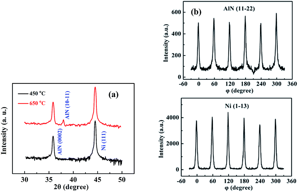 | ||
| Fig. 4 (a) Out-of-plane XRD 2θ–θ scan for AlN (0002) grown at 450 and 650 °C, respectively. (b) φ scans of AlN (112) and Ni (13), respectively. | ||
The temperature dependence of crystalline quality has been studied by X-ray rocking curves, as shown in Fig. 5a. We can clearly identify that the full width at half maximums (FWHMs) for AlN (0002) and (102) are 0.8° and 1.0° at growth temperature of 450 °C, respectively. The FWHMs are gradually decreased with the increase of growth temperature, ending up at 1.9° and 2.1° at growth temperature of 600 °C, respectively. Apparently, AlN grown on Ni (111) at lower temperature exhibits much higher crystalline quality. This can be tentatively attributed to the serious chemical reaction between AlN films and Ni atoms during the high temperature growth. The reaction leads to the formation of many dislocations in interfacial layer, extends into the films during the subsequent growth, and results in the poor film crystalline quality eventually.6,7,18
 | ||
| Fig. 5 (a) Temperature dependence of FWHMs, and (b) typical GIXR image for a about 95 nm-thick AlN films grown on Ni (111) substrates at 450 °C. | ||
The GIXR is introduced to further investigate the structural properties of AlN/Ni hetero-interfaces. Due to the fact that the GIXR measurement usually requires the thickness of thin films to be within 100 nm, we use thinner AlN films for this study as the ref. 19 and 20 Fig. 5b is the GIXR and its fitted curve for the as-grown about 100 nm-thick AlN films on Ni (111) substrates grown at 450 °C for 40 min.21–23 The fitted result has revealed that the thickness of as-grown AlN films is about 95 nm. There is no interfacial layer existing between AlN and Ni (111), and AlN surface RMS roughness is 1.1 nm, which are got from the GIXR measurement. However, when the growth temperature of AlN is increased to 600 °C, the interfacial layer thickness is increased to 2.5 nm also obtained from the GIXR measurement. Evidently, the growth temperature is of significant importance in achieving AlN films with high structural properties.
Cross-sectional TEM is applied to study the interfacial properties of AlN/Ni hetero-interfaces in detail. Fig. 6a is a bright field cross-section TEM image at low magnification for the interfaces between AlN and Ni grown at 450 °C, from which we can clearly find interfaces between AlN and Ni, as illustrated by the dashed lines. Meanwhile, we can also observe the thickness of the AlN films is 302 nm from Fig. 6a, as illustrated by two dashed lines. This result agrees well with the cross-sectional FESEM measurement. HRTEM is employed to further study the interface. We find that the whole interface between AlN film and Ni substrate is very homogeneous, sharp and abrupt, as shown in Fig. 6b, which indicates the high interfacial properties of AlN/Ni hetero-interfaces. However, as the increase in the growth temperature, the thickness of the interfacial layer increases gradually. The AlN films grown at high temperature of 600 °C show a thicker interfacial layer of 2.5 nm, as shown in Fig. 6c. These results are consistent well with the results measured by GIXR measurement. The formation of this interfacial layer may be ascribed to the chemical reaction between the AlN films and the Ni substrates during the initial growth process.8,18 After carefully studying the TEM image of Fig. 6b, we can obtain two in-plane epitaxial growth relationships of AlN[100]//Ni[11] and AlN[110]//Ni[10] between AlN films and Ni substrates.
 | ||
| Fig. 6 Cross-sectional TEM images for the interfaces of AlN films grown on Ni substrates. (a) A bright field cross-sectional TEM image at low magnification for the interface between AlN and Ni grown at 450 °C. HRTEM micrographs around the interfaces for AlN films grown at (b) 450, and (c) 600 °C, respectively. | ||
The pulsed laser provides high enough energy for the migration of AlN precursors on the Ni substrates, and thereby makes it possible for the films growth at low temperature. Furthermore, the growth at low temperature can effectively suppress the chemical reactions between AlN films and Ni substrates. It is known that the epitaxial growth direction between film and substrate is related to both the lattice mismatch and interfacial energy.24–26 In our case, the in-plane epitaxial relationship of AlN[110]//Ni[10] is formed, due to its lower interfacial energy despite the larger lattice mismatch.24–26 This epitaxial relationship is much easier for the nucleation of AlN film on the Ni surface. Therefore, it makes the growth of AlN films possible without the formation of interfacial layer.
In order to further study the strain state in as-grown about 300 nm-thick AlN films, the RSMs of AlN (0002) and AlN (105) are conducted. Fig. 7a is the RSM of AlN (0002), where one can find that the AlN (0002) is located below the Ni (111) in the reciprocal space. This result once again confirms the epitaxial relationship between AlN films and Ni substrates is AlN (0001)//Ni (111). Furthermore, the lattice parameters for AlN films are aAlN = 3.091 nm and cAlN = 0.4991 nm,20,27 respectively, can be obtained from Fig. 7b. Since the lattice parameters for fully relaxed AlN are aAlN = 3.112 nm and cAlN = 0.4982 nm, respectively, the as-grown AlN film is about 0.67% compressive along its a-axis, and is about 0.18% tensile along its c-axis.20 In this regard, almost fully relaxed AlN films are achieved on Ni substrates.
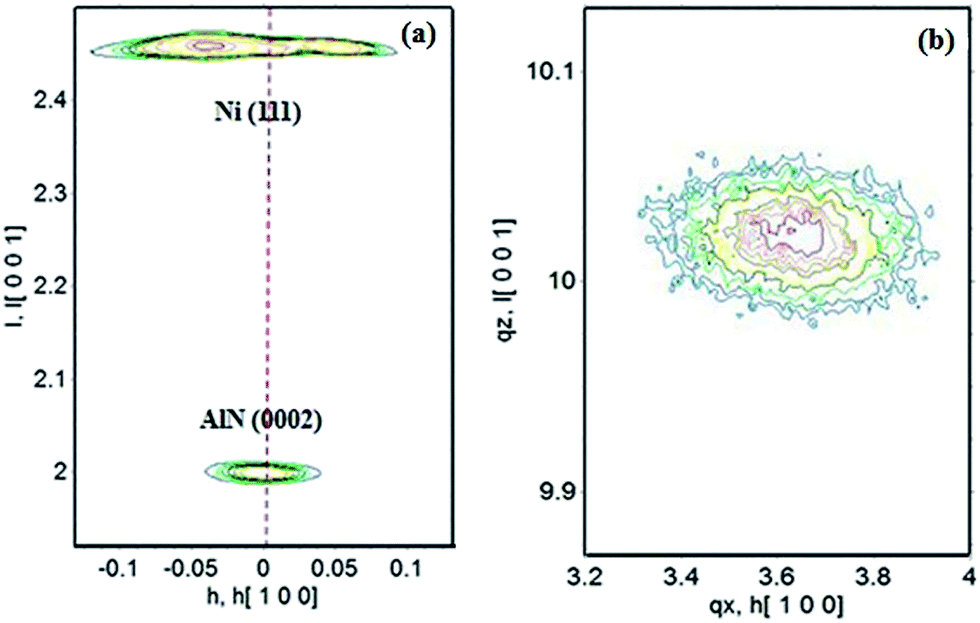 | ||
| Fig. 7 RSMs of (a) AlN (0002) and (b) AlN (105) for the about 300 nm-thick AlN films grown on Ni (111) substrates at the growth temperature of 450 °C. | ||
Due to the lattice mismatch, there is strain existing in the AlN films, which leads to the formation of defects, mainly dislocations, during the films growth.20 The dislocations will annihilate by the formation of dislocation loops, the changes of the direction of dislocation motion and dislocation reactions, etc., during the further growth of AlN films.28,29 In other words, the formation of dislocations results in the release of lattice mismatch strain. During the cooling process, the difference in thermal expansion coefficient between AlN films and Ni substrates would result in the formation of strain in AlN films.20,25,26 Furthermore, the formed strain will be released by the formation of dislocations.20 In this case, as the AlN films are cooled down to the room temperature, there is still a compressive strain of 0.67% existing in AlN films.
Evidently, high-quality AlN films have been grown on Ni (111) substrates by pulsed laser deposition at low temperature. Although high-quality AlN films have been grown on metallic Ni substrates, future work should be focused on the preparation of AlN-based device with these high-quality AlN films.
4. Conclusion
In summary, single-crystalline AlN films on Ni (111) substrates have been epitaxially grown and characterized. It can be found that AlN films grown on Ni (111) substrates at 450 °C reveal very smooth surface with a RMS roughness of 1.0 nm, while AlN films grown at higher temperature of 650 °C exhibit many disordered particulates or hillocks with a RMS roughness of 5.7 nm. Typical 2θ–θ scan of AlN (0002), and φ scans of AlN (112) and Ni (13) have revealed the out-of-plane and in-plane epitaxial growth relationships of AlN (0001)//Ni (111), and AlN[110]//Ni[10], respectively. GIXR measurement has revealed that there is no interfacial layer exiting between AlN and Ni at the growth temperature of 450 °C, which is confirmed by the cross-sectional TEM measurement. RSM measurements have found that the as-grown about 300 nm-thick AlN films grown at 450 °C are almost fully relaxed only with an in-plane compressive strain of 0.67%, and an out-of-plane tensile strain of 0.18%. We attribute these results mainly to two aspects. One is the low temperature growth, and the other is the utilization of PLD technique. The former can effectively suppress the interfacial chemical reactions between the AlN films and Ni substrates and is beneficial to the films growth. The latter can provide high kinetic energy and assist the migration of the precursors on the surfaces, then make the films growth at low temperature possible. These AlN films are of significant importance for the potential applications of AlN-based devices which ask for the flat surface and abrupt interface between AlN films and metal substrates.
Acknowledgements
This work is supported by National Natural Science Foundation (no. 51372001), Excellent Youth Foundation of Guangdong Scientific Committee (no. S2013050013882), Key Project in Science and Technique of Guangdong Province (no. 2011A080801018), and Strategic Special Funds for LEDs of Guangdong Province (nos 2011A081301010 and 2011A081301012).References
- Q. Peng, X. J. Chen, S. Liu and S. De, RSC Adv., 2013, 3, 7083–7092 RSC
.
- W. L. Wang, Y. H. Lin, W. J. Yang, Z. L. Liu, S. Z. Zhou, H. R. Qian, F. L. Gao, L. Wen and G. Q. Li, J. Mater. Chem. C, 2014, 2, 4112–4116 RSC
- G. J. Yan, G. D. Chen, K. Sun, B. L. Jiang, K. Zhao and N. Tian, RSC Adv., 2014, 4, 6840–6484 RSC
- W. J. Yang, W. L. Wang, Y. H. Lin, Z. L. Liu, S. Z. Zhou, H. R. Qian, F. L. Gao, S. G. Zhang and G. Q. Li, J. Mater. Chem. C, 2014, 2, 801–805 RSC
- S. S. Li, C. W. Zhang, R. W. Zhang, P. Li, F. Li, M. Yuan, M. J. Ren, W. X. Ji and P. J. Wang, RSC Adv., 2014, 4, 7500–7505 RSC
- H. Yang, W. L. Wang, Z. L. Liu and G. Q. Li, J. Phys. D: Appl. Phys., 2013, 46, 105101 CrossRef
- G. Q. Li, T. W. Kim, S. Inoue, K. Okamoto and H. Fujioka, Appl. Phys. Lett., 2006, 89, 241905 CrossRef PubMed
- H. Yang, W. L. Wang, Z. L. Liu and G. Q. Li, CrystEngComm, 2013, 15, 7171–7176 RSC
- T. F. Chen, Y. Q. Wang, P. Xiang, R. H. Luo, M. G. Liu, W. M. Yang, Y. Ren, Z. Y. He, Y. B. Yang, W. J. Chen, X. R. Zhang, Z. S. Wu, Y. Liu and B. J. Zhang, Appl. Phys. Lett., 2012, 100, 241112 CrossRef PubMed
- Y. J. Sun, T. J. Yu, C. Y. Jia, Z. Z. Chen, P. F. Tian, X. N. Kang, G. J. Lian and G. Y. Zhang, Chin. Phys. Lett., 2012, 27(2), 127303 Search PubMed
- L. Liu and J. H. Edgar, Mater. Sci. Eng., R, 2002, 37, 61–127 CrossRef
- R. C. Dorf, Handbook of engineering tables, CRC Press LLC, Boca Raton, London, New York, Washington, D.C., 2003, p. 200 Search PubMed
- S. Inoue, K. Okamoto, N. Matsuki, T. W. Kim and H. Fujioka, Appl. Phys. Lett., 2006, 88, 261910 CrossRef PubMed
- M. N. R. Ashfold, F. Claeyssens, G. M. Fuge and S. J. Henley, Chem. Soc. Rev., 2004, 33, 23–31 RSC
- D. H. Kim, L. Bi, N. M. Aimon, P. Jiang, G. F. Dionne and C. A. Ross, ACS Comb. Sci., 2012, 14, 179–190 CrossRef CAS PubMed
- M. Spreitzer, R. Egoavil, J. Verbeeck, D. H. A. Blank and G. Rijnders, J. Mater. Chem. C, 2013, 1, 5216–5222 RSC
- J. Ohta, H. Fujioka, M. Sumiya, H. Koinuma and M. Oshima, J. Cryst. Growth, 2001, 225, 73–78 CrossRef CAS
- W. L. Wang, H. Yang and G. Q. Li, CrystEngComm, 2013, 15, 2669–2674 RSC
- W. L. Wang, W. J. Yang, Z. L. Liu, Y. H. Lin, S. Z. Zhou, H. R. Qian, F. L. Gao, H. Yang and G. Q. Li, Appl. Surf. Sci., 2014, 294, 1–8 CrossRef CAS PubMed
- M. A. Moram and M. E. Vickers, Rep. Prog. Phys., 2009, 72, 036502 CrossRef
- L. G. Parratt, Phys. Rev., 1954, 95, 359–369 CrossRef
- L. Névot and P. Croce, Rev. Phys. Appl., 1980, 15, 761–779 CrossRef
- W. L. Wang, W. J. Yang, Z. L. Liu, Y. H. Lin, S. Z. Zhou, H. R. Qian, F. L. Gao and G. Q. Li, CrystEngComm, 2014, 16, 4100–4107 RSC
- S. Inoue, K. Okamoto, N. Matsuki, T. W. Kim and H. Fujioka, J. Cryst. Growth, 2006, 289, 574–577 CrossRef CAS PubMed
- W. L. Wang, S. Z. Zhou, Z. L. Liu, W. J. Yang, Y. H. Lin, H. R. Qian, F. L. Gao and G. Q. Li, Mater. Res. Express, 2014, 1, 025903 CrossRef
- Y. W. Pohl, Epitaxy of Semiconductors, Springer, New York, 1st edn, 2013 Search PubMed
- W. L. Wang, H. Yang and G. Q. Li, J. Mater. Chem. C, 2013, 1, 4070–4077 RSC
- M. A. Moram, C. S. Ghedia, D. V. S. Rao, J. S. Barnard, Y. Zhang, M. J. Kappers and C. J. Humphreys, J. Appl. Phys., 2009, 106, 073513 CrossRef PubMed
- R. A. Oliver, S. E. Bennett, T. Zhu, D. J. Beesley, M. J. Kappers, D. W. Saxey, A. Cerezo and C. J. Humphreys, J. Phys. D: Appl. Phys., 2010, 43, 354003 CrossRef
| This journal is © The Royal Society of Chemistry 2014 |