Xudong Guo,
Haopeng Dong,
Guangda Niu,
Yong Qiu and
Liduo Wang*
Key Lab of Organic Optoelectronics & Molecular Engineering of Ministry of Education, Department of Chemistry, Tsinghua University, Beijing 100084, China. E-mail: chldwang@mail.tsinghua.edu.cn
First published on 30th April 2014
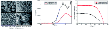
In this paper, Mg doping is utilized in the synthesis of a nanosheet-based spherical structured ZnO photoanode resulting in an increased overall efficiency from 1.72% to 4.19% of quasi-solid dye-sensitized solar cells. Existence of Mg in the ZnO crystal is detected by XRD and XPS measurements. The diameter of the ZnO nanosheet-based spherical structure is obviously decreased after Mg doping, which facilitates the fabrication of ZnO films and increases the specific area leading to larger dye loading and higher photocurrent. The energy bandgap of the ZnO photoanode with and without Mg doping is investigated by UV-vis spectra and theoretical calculation based on the GAUSSIAN 09 program and an increase of the bandgap is observed after Mg doping, which leads to an increase of the conduction band position and enhances the photo-voltage of DSSCs based on Mg doped ZnO photoanodes. An electrochemical impedance spectroscopy (EIS) test also indicates that DSSCs based on Mg doped ZnO show a strengthened effect of facilitating electron transport and retarding the charge recombination.
Hierarchical structured ZnO such as nanocrystalline aggregates,11 dendritic nanowires12 and flower-like spheres13 have been reported in recent years. Nanosheet-based spherical structured ZnO can be synthesized by the following methods: hydrotherm,14 chemical bath deposition,15 electrodeposition,16 direct precipitation,17 and so on. Among these methods, one-step direct precipitation is the simplest approach and DSSCs based on nanosheet-based spherical structure ZnO synthesized by this method have been proved to reach high efficiency.18 However the size of nanosheet-based ZnO spheres synthesized by direct precipitation is about 4–5 μm,18 which is too large that the ZnO spheres are easy to assemble together and can't form homogenous and smooth films. Thus, ZnO nanoparticles (10–20 wt%) about 20 nm in diameter are needed to blend together with nanosheet-based spherical structured ZnO to increase the mechanic strength of the photoanodes, which made the process complicated.
In addition to morphology controlling of ZnO, the metal doping is also an alternative method to improve the DSSCs' performance.19–23 Doped ZnO thin films exhibit relatively low resistivity, high transmittance and chemical stability when compared with pure ZnO thin films. Former work has reported a banyan root like Mg-doped ZnO photoanode based DSSCs' conversion efficiency of 4.11% under 1 sun illumination.24 However, in that work, Mg doping is achieved by the introduction of the appropriate amount of magnesium acetate dihydrate and zinc acetate adding into 2-methoxyethanol and monoethanolamine, which may lead to the formation of ZnO and MgO separately, thus weaken the effect of Mg doping.
Here we report a new method to synthesis Mg doped nanosheet-based spherical structured ZnO and fabricated DSSCs. In this work, Zn2+ is firstly reacted with OH− forming [Zn(OH)4]2−, then mixed with Mg2+ to form Mg doped ZnO. By Mg doping, the diameter is obviously reduced, which facilitates the formation of ZnO films and simplifies the photoanode fabrication process. The photo-electric properties of ZnO DSSCs such as photocurrent and photo-voltage are obviously improved after Mg doping and the reasons for these improvements are investigated in this paper. Quasi-solid electrolytes were used here to avoid the problems such as electrolyte leakage, volatilization and corrosion that limiting the long-term performance of the DSSCs assembled using liquid electrolytes.18
(1 − x)[Zn(OH)4]2− + xMg(Ac)2 = Zn1−xMgxO + 2xAc− + H2O + (2 − 4x)OH− | (1) |
[Zn(OH)4]2− = ZnO + H2O + 2OH− | (2) |
The reaction rate in eqn (2) is very low but in eqn (1) the acid magnesium acetate can act as the reaction center to congregate [Zn(OH)4]2−, which quickens the reaction. Fig. 2 shows the formation process of ZnO with Mg doping and without Mg doping. In the Mg2+ absent system, the repulsion between [Zn(OH)4]2− makes the process of ZnO crystal nucleus formation slow and only a few ZnO crystal nucleus generate. When adding Mg2+ in to this system, Mg2+ would attract the OH− of [Zn(OH)4]2− because the solubility product (Ksp) of Mg(OH)2 is only 1.8 × 10⁻¹¹. As a result, the equilibrium in the [Zn(OH)4]2− is broken rapidly and a large amount of Zn1−xMgxO crystal nucleus appears. As the quantity of [Zn(OH)4]2− is equal in both these two systems, the ZnO nanoparticle is much larger in the Mg2+ absent system as showed in Fig. 2. As for the nanosheet structure, the driving forces to assemble nanocrystals are anisotropic hydrophobic attraction and electro-static interactions derived from dipole moments or surface charges, which makes ZnO form nanosheet structure.18
![]() | ||
Fig. 2 Schematic diagram of ZnO formation process with Mg doping (top) and without Mg doping (bottom). |
Fig. 3a shows the X-ray diffraction patterns of Mg doped ZnO and pure ZnO films on FTO substrate. As seen in this figure, the films are polycrystalline with hexagonal wurtzite structure without any new phase due to the addition of Mg. The shift of the corresponding (002) peak toward higher angle (Fig. 3b) is mainly due to the incorporation of Mg ions in the interstitial sites of wurtzite structure. The ion radius of Mg2+ is less than that of Zn2+, which would decrease the spacing of ZnO crystal. According to the Braggs formula:
2d![]() ![]() | (3) |
![]() | ||
Fig. 3 (a) XRD pattern of ZnO with and without Mg doping on FTO substrate. (b) Shift of (002) peak position of ZnO with and without Mg doping. |
XPS was measured to investigate the composition and chemical bond configuration of pure and Mg doped ZnO thin films. Fig. 4 is the typical XPS survey spectra of pure and Mg doped ZnO thin films, showing the Mg 1s binding energy peak at 1304.27 eV in the Mg doped ZnO thin film but no such peak in pure ZnO films, which confirmed that Mg was doped into the ZnO. By integrating the XPS peak area, the atomic percent of Mg and Zn is 3.73% and 43.78%, respectively. That means after reaction, the mole percent of Mg increased from 2% to about 8%. In eqn (4), the Zn(OH)42− can't react completely because increase of OH− would retard this reaction moving forward.
N3 adsorption/desorption is used to detect the specific area of the photoanodes based on two samples and the results are shown in Table 1. We can see that after Mg doping, specific areas of the samples increased from 16.83 m2 g−1 to 37.12 m2 g−1, in accordance with their particle sizes, proving that Mg doping can increase nanosheet-based spherical ZnO' specific areas on a large scale.
Samples | Specific area/m2 g−1 | Dye-loading/nmol cm−2 |
---|---|---|
ZnO | 16.83 | 104 |
Mg doped ZnO | 37.12 | 155 |
The amount of dye adsorbed on ZnO and Mg doped ZnO electrodes is estimated by desorbing the dye from sensitized ZnO photoanode using sodium hydrate. Compared to pure ZnO film (Fig. 5), Mg doped ZnO electrodes shows an increased dye adsorption. Detailed data is listed in Table 1. The dye-loading of pure ZnO is 104 nmol cm−2 and increased to 155 nmol cm−2 after Mg doping. This larger dye adsorption in Mg doped ZnO will lead to a higher photocurrent when fabricated DSSCs. However, the value of specific area is not proportionate to that of dye-loading. That is because the resistance of ZnO electrode surface to acidic dye increased after Mg doping.24
![]() | ||
Fig. 5 UV-vis absorbance spectra of solutions containing dyes desorbed from the sensitized photoanodes composed of ZnO with and without Mg doping. |
According to former research, the optical band gap (Eg) of metal oxide semiconductor Eg for the absorption edge and the absorption coefficient (A) near the photo absorption edge has a relationship complied with the following formula:24
(Ahv)2 = c(hv − Eg) | (4) |
From eqn (4) we can find that the Eg for the absorption edge can be obtained by fitting linear portion (3.25 eV to 3.31 eV for undoped ZnO and 3.29 eV to 3.32 eV for Mg doped ZnO) with least square method. The correlation coefficients are 0.985 and 0.991 respectively. In Fig. 6, after Mg doping, the bandgap of ZnO increases from 3.23 eV to 3.27 eV indicating a 0.04 eV's rise of the ZnO photoanode's conduction band position. The photo-voltage of a DSSCs corresponds to the difference of the quasi-Fermi level of electrons in the photoanode under illumination and the Nernst potential of the electrolyte. As the Nernst potential of the electrolyte remains the same, the photo-voltage increases because of the rise of the conduction band after Mg doping.
Furthermore, we execute theoretical calculation to investigate the band gap change of Mg doped ZnO. Calculations are performed with the help of DFT at the B3LYP level and the GAUSSIAN 09 program.25 The B3LYP functional24 has been shown to provide realistic bulk band gap energies of metal oxides, and is thought to work well also for nanosized clusters. Both Zn atoms and O atoms are presented by the 6-31+g* basis set, which includes one polarized26 and one diffused function.27 Because the atomic percent of Mg and Zn is 3.73% and 43.78%, the real atomic ratio between Mg and Zn is about 1:
11. According to this ratio, the following three initial configurations were choosen, which is built from cutting wurtzite–ZnO crystal, comes from Zhao et al.'s work to design and character ZnO clusters.28 Fig. 6 shows the optimized configuration. The calculated Mg doped ZnO's HOMO–LUMO gap (band gap) increases from 3.79 eV to 3.84 eV (Fig. 7a's configuration) and 3.85 (Fig. 7b's configuration), indicating a 0.05–0.06 eV's rise of the ZnO photoanode's conduction band after Mg doping. This increment corresponds to the value investigated by UV-vis DRS spectra very well and will express on the photo-voltage's increase of DSSCs in the next section.
![]() | ||
Fig. 8 Current–voltage (I–V) characteristics of DSSCs based on a ZnO film with and without Mg doping. |
Samples | Jsc/(mA cm−2) | Voc/V | FF% | η% |
---|---|---|---|---|
ZnO | 6.08 | 0.56 | 50.1 | 1.72 |
Mg doped ZnO | 11.18 | 0.60 | 62.5 | 4.19 |
To investigate the reasons for a higher photocurrent result for DSSCs based on Mg doped ZnO, we measured the monochromatic incident photon-to-current conversion efficiency (IPCE) to study the photoactive wavelength regime for the pure and doped ZnO cells. The IPCE value is the percentage of photons hitting the device's photoreactive surface that produce charge carriers at FTO. At approximately 520 nm, there is an obvious enhancement of Mg doped ZnO's IPCE value compared to the pure ZnO's value, which is attributed to the more dye adsorption and less recombination of electrons with the electrolyte mainly due to the larger resistance at the interface of photoanode and the electrolyte.
In order to estimate the resistance of electron transport and charge recombination processes in Mg doped and pure ZnO DSSCs, we have measured the electrochemical impedance spectra (EIS) under fixed illumination of 100 mW cm−2. The Nyquist plots of the DSSCs under dark and sun condition are shown in Fig. 10, where the equivalent circuit of the DSSCs is inserted. On the equivalent circuit, the series resistance (RS) includes the FTO electrode and external circuit while other three impedance units represent resistances (R1, R2, R3) and constant phase elements (CPE1, CPE2). The diameters of the semicircles (Fig. 10) at high, intermediate, and low frequency ranges represent R1, R2, and R3, corresponding to the resistances for the charge transfer at the counter electrode, the electron transport/charge recombination at the ZnO/electrolyte interface, and the diffusion of I3− ions in the electrolyte, respectively.29
Fig. 10a shows the Nyquist plots of devices based on ZnO and Mg doped ZnO at open-circuit voltage in dark condition, where the diameter of middle frequency semicircle represents the resistance of at the sensitized Mg doped ZnO/electrolyte interface. Compared with pure ZnO, the interface resistance (R2) of Mg doped ZnO based DSSCs is larger, which means the charge recombination at the ZnO/dye/electrolyte interface is obviously retarded and as a result to improve the electron collection. The decrease of recombination is mainly caused by an increase in electron lifetime supports reduction in the recombination of injected electrons with the I3− in the electrolyte.24 Under illumination condition, the DSSCs could be taken as diodes and resistance at the ZnO/dye/electrolyte interface is also presented by the middle frequency semicircle in the Nyquist plots.30 As shown in Fig. 10b, The smaller the diameter of middle frequency semicircle shows a smaller interface resistance and a faster electron injection at the sensitized Mg doped ZnO/electrolyte interface, which is supposed to be the main reason an increase in fill factor from 50.1% to 62.5%. Thus the enhanced injection electron can raise the photo-current and IPCE, which accorded with the results shown in Fig. 8, 9 and Table 2.
This journal is © The Royal Society of Chemistry 2014 |