The effect of microstructure and metal-oxide barriers on carrier transport in top-down processed, low density nanograined n-type PbTe

P. K. Rawat and P. Banerji*
Materials Science Centre, Indian Institute of Technology, Kharagpur 721302, India. E-mail: pallab@matsc.iitkgp.ernet.in

Received 27th March 2014 , Accepted 16th June 2014

First published on 17th June 2014


Abstract

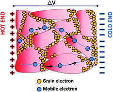
The combined effects of microstructure and interfacial metal-oxide barriers at grain boundaries on carrier transport in top-down processed, nanogranular n-type bulk PbTe have been investigated. It is found that the porous nature of the microstructure leads to significantly reduced thermal conductivity. Naturally occurring metal-oxide potential barriers at the PbTe grain interface result in notably reduced Hall carrier concentration and significantly enhanced resistivity with non-degenerate temperature dependence; they also incorporate additional carrier scattering along with acoustic phonons in the material system. Further, our investigation shows that unlike Hall carrier concentration and resistivity, thermopower is not an inherent property of the bulk granular solid but of its constituent grains.


Introduction

PbTe is a highly efficient and particularly well studied thermoelectric material in the lead chalcogenide (S, Se, Te) family for mid-range power generation applications.1,2 The dimensionless parameter zT, expressed as image file: c4ra02701a-t1.tif (where S is the thermopower, ρ is the electrical resistivity, T is the absolute temperature, and κl and κe are the lattice and electronic thermal conductivities, respectively) and known as the thermoelectric figure of merit, reflects the power conversion efficiency of a particular class of material.3–5 For efficient power conversion, the power factor image file: c4ra02701a-t2.tif should be enhanced, with simultaneous reduction in the total thermal conductivity, κ(=κl + κe). However, it is very hard to tailor and disconnect the linkage between the interconnected transport parameters (i.e. S, ρ, and κ).6 The interconnection between various thermoelectric transport parameters has recently been demonstrated effectively in a Yb-doped PbTe system.7 It was found that upon incorporating various carrier scattering modes and mechanisms into the material system, one could quasi-independently vary the thermoelectric transport parameters. Recent works of Zebarjadi et al.8 and Yu et al.9 showed a significant reduction in thermal conductivity with minimal effect on the electrical resistivity and thermopower in SiGe alloys using a modulation doping mechanism. Various research groups also demonstrated the similar quasi-interdependence of the parameters by band structure engineering, such as by heavy hole-dominated conduction,10,11 energy barrier filtering,12–19 optimization of carrier concentration,20–22 etc. Heremans et al.23 showed a significant enhancement in thermopower by incorporating a resonant impurity, viz. Tl, in the host (PbTe) conduction band. Using the same approach of density-of-states modification by resonant impurities, Jaworski et al.24 and Zhang et al.25 reported similar enhanced effects in Bi2Te3 and PbSe by Sn and Al inclusion, respectively. Since κl is the only parameter that is independent of the other, interdependent parameters in zT, a lot of effort has been given to reducing the value of this entity for higher thermoelectric efficiency by scattering of phonons via nanostructuring26–30 and at the interfaces of grain boundaries.31 It has been observed that the boundaries and interfaces in thermoelectric materials (of all scales) influence all three thermoelectric parameters, i.e. S, ρ, and k very significantly, and they play a critical role in tailoring the transport process for optimized thermoelectric performance.31 Though these boundaries and interfaces in the granular nanostructured materials reduce κl to a significant level compared to their melt-grown counterpart, and the filtering of low-energy charge carriers enhances S,32,33 the resulting enhanced interfacial carrier scattering usually leads to an increase in ρ. Kishimoto and Koyanagi32 observed a notable rise in S in sintered n-type degenerate PbTe by potential barrier scattering that occurs at the grain boundaries when the grain size is reduced from 4 to 0.7 μm. However, a significant reduction in electrical and thermal conductivity was also observed. In similar ways, Nolas and coworkers13,33 showed similar enhancement in S in p-type PbTe nanocomposites. Further, the measurements of Heremans et al.16 demonstrated a larger energy dependence of carrier relaxation time in nanocrystalline PbTe than that of the bulk material, which justifies the filtering of low-energy charge carriers in the nanocrystalline material system, causing enhancement in S. It is general practice to synthesize highly dense (>95% bulk theoretical density) nanogranular bulk materials for thermoelectrics by the chemically driven, bottom-up approach using spark plasma sintering (SPS) or hot pressing for the consolidation of nano-crystalline grains.31 However, low density materials could be more advantageous for achieving significantly reduced κ, though its consequences on other transport parameters in zT need to be investigated. Recently, Lee et al.34 reported a significant reduction in thermal conductivity in nanoporous Si than that of its bulk counterpart. In the literature, no detailed experimental investigation has been reported on the combined effect of microstructural porosity and interfacial structure between the grains on the carrier transport in top-down processed, n-type bulk PbTe. Therefore, in the present investigation, we explored the effect of microstructure and grain boundary scattering on the carrier transport in nanograined n-type PbTe.

Experimental

For the investigation, 5 N pure Pb (Alfa Aesar) and Te (Sigma Aldrich) were measured at a stoichiometric ratio of 1[thin space (1/6-em)]:[thin space (1/6-em)]1 into a carbon-coated, fused silica ampoule and sealed under high vacuum (∼10−5 Torr). 5 N pure PbI2 (Sigma Aldrich) was used as n-type dopant for PbTe. Then the sealed ampoule was placed in a vertical furnace at 1273 K for 7 h. After cutting a slice (S1), the obtained ingot was ground into powder form, and in order to get grains of different size, samples were collected at three different grinding times (GT) and subsequently cold-pressed at 9 Ton pressure using a stainless steel die of 12 mm diameter. Three discs, viz. D1 (GT-30 min), D2 (GT-45 min), and D3 (GT-60 min), each of 12 mm diameter, were obtained by the process. The discs (D1, D2, and D3) were sintered under Ar atmosphere for 90 minutes at 923 K and then mechanically lapped (including S1) with 5 μm silicon carbide (SiC) powder; then they were polished with alumina (Al2O3) abrasive for X-ray photoelectron spectroscopy (XPS) and Hall, resistivity, and thermal measurements. The Hall and resistivity measurements were done under van der Pauw geometry. Room temperature (300 K) thermal measurements were done using a hot disk TPS 2500 S instrument. Afterwards, the samples were cut diagonally into bar shapes with dimensions 1.5 × 1.5 × 10 mm3 for thermopower measurements using an in-house built instrument described elsewhere.35 Crystal structures of the samples were obtained by powder X-ray diffraction (XRD) using Cu-Kα radiation under reflection geometry on a PANalytical diffractometer operated at 40 kV and 30 mA. Surface morphology of the fractured surface of the samples was acquired by scanning electron microscopy (SEM) using a ZEISS EVO 60 Scanning Electron Microscope. Transmission electron microscopic (TEM) images and selected area electron diffraction (SAED) patterns were obtained at 200 keV using a FEI-TECNAI G2 20S-TWIN microscope. The sample for TEM investigation of S1 was prepared by conventional methods of lapping, ultrasonic disc cutting, dimple grinding, and ion milling. TEM studies for ground materials were done using copper-grid supported samples. XPS spectra were obtained using an ESCALAB MK II spectrometer with an Al-Kα source.

Results and discussion

The powder X-ray diffraction pattern of as-grown bulk ingots and their corresponding ground powders (Fig. 1) depicts the formation of the face-centered-cubic (fcc) phase of the PbTe structure (Fm[3 with combining macron]m space group), with lattice parameter value of 6.463 Å. No impurity peaks of other phases were observed.
image file: c4ra02701a-f1.tif
Fig. 1 Powder X-ray diffraction patterns of melt-grown, n-type PbTe ingots and their corresponding ground powders.

Fig. 2 shows the transmission electron microscopic image of the sample S1 (a) and ground material (b). The TEM image of a selected portion of sample S1 shows good long-range crystallinity. The spot pattern of the selected area's electron diffraction [shown in Fig. 2(c)] also reveals the long-range order (single crystallinity) of the grains in this sample. However, Fig. 2(b) shows distortion in the long-range order and indicates the existence of mixed domains of crystalline and amorphous regions in the ground material. Due to the resolution limitation, the amorphous domains could not be identified by the XRD pattern. The mixed picture of the spotted and diffused rings in the SAED pattern of the ground material [shown in Fig. 2(d)] further indicates the polycrystalline-amorphous nature of the lattice.


image file: c4ra02701a-f2.tif
Fig. 2 Transmission electron micrograph and SAED pattern of S1 [(a) &(c)] and the ground material [(b)&(d)].

Fig. 3 shows the field emission scanning electron (FESEM) micrographs of the fractured surfaces of S1 (a), D1 (b), D2 (c), and D3 (d). It is clearly seen from Fig. 3 that the average grain size of D1 > D2 > D3. This change in microstructure is due to the different grinding times of the constituent PbTe ingot. However, in S1 no such grains are visible, which indicates a highly dense microstructural morphology (close to the theoretical density) in this particular sample. To determine the degree of density change in ground samples with respect to S1, the densities of all the samples were determined by the Archimedes method and are tabulated in Table 1.


image file: c4ra02701a-f3.tif
Fig. 3 Scanning electron micrograph of (a) S1, (b) D1, (c) D2, and (d) D3.
Table 1 Sample density and room-temperature (300 K) values of measured transport parameters
Sample Density (g cm−3) Thermal conductivity (Wm−1 K−1) Resistivity (Ω cm) Hall carrier concentration (cm−3) Mobility (cm2 V−1 s−1) Thermopower (μV K−1)
S1 8.19 4.212 2.8 × 10⁻⁴ 3 × 10¹⁹ 736 58
D1 5.31 1.811 0.6 7 × 10¹⁵ 1471 170
D2 5.56 1.629 1.6 5 × 10¹⁵ 731 193
D3 5.67 1.604 3.9 3 × 10¹⁵ 523 219


Fig. 4 presents the XPS spectra of sample S1 (a) and D1 (b). The appearance of O 1s peaks and second-component peaks in the Pb 4f and Te 3d spectra of both samples indicate naturally occurring oxygen adsorption at the PbTe surface. The chemical shifts in the second-component peaks obtained from the Pb 4f and Te 3d spectra are found to be +1.01, +3.82 and +0.92, +3.55, respectively, in samples S1 and D1. During measurement, because of the sample charging effect in D1 (caused by the low electrical conductivity), the Pb 4f peak is found to be situated at a slightly higher binding energy in comparison to sample S1. However, the oxide content in the ground material is expected to be higher than that of S1, as more surface area was exposed to air during grinding. The higher coverage area of the second-component peaks in the XPS spectra further shows the potent presence of oxide complexes at the PbTe surface. This significant presence of oxide complexes suggests the formation of a thin dielectric layer at the PbTe material surface. On the basis of the XPS database, the oxides were assigned as metal oxides of Pb (PbO) and Te (TeO2), and the peaks obtained correspond to Pb2+ and Te4+ oxidation states, respectively.


image file: c4ra02701a-f4.tif
Fig. 4 X-ray photoelectron spectra of sample (a) S1 and (b) D1.

The room-temperature values of various transport parameters in samples S1, D1, D2, and D3 are listed in Table 1. Due to high porosity (that results in enhanced scattering of the thermal carriers, i.e. the phonons), all the powder-processed samples exhibited significantly reduced thermal conductivities than that of sample S1, and these were found to moderately decrease with the grinding time. This inverse relationship between the thermal conductivity and grinding time can be explained by the enhanced phonon scattering due to the increased effective surface-to-volume ratio of the grains.

The temperature-dependent resistivity of each sample is shown in Fig. 5. Samples D1, D2, and D3 show significantly higher resistivity throughout the investigated temperature range than sample S1, which could be explained by the porous nature of the samples.35 The gradual fall in resistivity in D1, D2, and D3 indicates non-degenerate transport of the charge carriers. However, the gradual rise in resistivity in S1 shows degenerate charge transport, which is typical in highly dense, PbI2-doped PbTe.36 As shown in Table 1, the room-temperature Hall carrier concentrations in the powder-processed samples were reduced by several orders of magnitude (thus the resistivity was increased several times) compared to sample S1 and moderately decreased with grinding time.


image file: c4ra02701a-f5.tif
Fig. 5 Temperature variation of electrical resistivity in S1 and powder-processed samples.

Fig. 6 shows the temperature dependence of Hall carrier concentration in all the samples. The carrier concentration is found to be significantly lower throughout the investigated temperature range in powder-processed samples compared to sample S1, though the dopant concentration (PbI2) is the same in all the samples. The slight gradual decrease in carrier concentration with rise in temperature in S1 is caused by the minute loss of degeneracy at elevated temperatures.36 However, other samples (D1, D2, and D3) show progressive enhancement in Hall carrier concentration with temperature, which could be the reason for the observed non-degenerate transport in such samples (Fig. 5). The reason for such temperature dependence and dramatically low values of Hall carrier concentrations in D1, D2, and D3 can be explained by the formation of dielectric potential barriers of PbO and TeO2, due to the oxidation of the grain surfaces at the grain boundaries.13,33,37 Martin et al.33 reported the formation of such oxide barriers by oxygen adsorption in PbTe nano-composites due to the aqueous method of synthesis. In the present case, the observed oxidation of grain surfaces in normal air ambience also indicates high surface reactivity of PbTe with oxygen, even though the solid-state synthesis method was used. This surface reactivity of PbTe with oxygen (surface oxidation) forms electron-trapping centers at the grain boundaries and also restricts the conduction of free carriers between the grains, resulting in loss of electron carrier concentration.38,39 The increased number of grains (and thus the grain boundaries) introduced by higher grinding time incorporates more electron trapping centers in the samples; due to this, carrier concentration moderately decreases with grinding time. The monotonic increase in carrier concentration in D1, D2, and D3 is caused by the increased probability of thermionic emission of electrons over the energy barrier and tunneling through the barrier with the rise in temperature (because of increase in average thermal energy of the charge carriers).13,40 It is also worth noting that if the charge carriers are barrier-arrested (as in the present case, confined inside the grains by the dielectric layer), they could not contribute to the conduction; thus, the carrier concentration obtained by Hall measurement is not the actual carrier concentration within the grains, but the overall mobile carriers (thermionically emitted or tunneled) in the solid.


image file: c4ra02701a-f6.tif
Fig. 6 Temperature-dependent Hall carrier concentration for each sample.

Fig. 7 shows temperature-dependent mobility in all the samples. The observed high mobility in D1 is due to the significantly low value of the carrier (Hall) concentration, i.e. mobile charge density, in sample D1 (n = 7 × 1015 cm−3) compared to that in sample S1 (n = 3 × 1019 cm−3). The carrier mobility in pristine n-type PbTe is reported as 2000 cm2 V−1 s−1 for a carrier concentration value of 2 × 1018 cm−3;36 higher values of mobility are expected at lower carrier concentrations. However, in D1, the room-temperature mobility value is found to be 1471 cm2 V−1 s−1, though the Hall carrier concentration in this sample is ≪ 2 × 1018 cm−3, which indicates significant loss in carrier mobility caused by the porous nature of the sample. Due to increased interfacial scattering (potential barriers) of the charge carriers at the grain boundaries by the increased surface-to-volume ratio of the grains in D2 and D3, mobility was reduced in these samples compared to D1.


image file: c4ra02701a-f7.tif
Fig. 7 Temperature-dependent mobility in S1, D1, D2, and D3.

In contrast to sample S1, in which the mobility is found to monotonically decrease with temperature, D1, D2, and D3 show an anomalous increasing trend at the higher temperature range. In S1, the value of the exponent (δ) in the power dependence of mobility, i.e. μTδ, is found to be ∼1.5, which indicates domination of acoustic phonon scattering in the charge transport process.41 The values of δ in D1, D2, and D3 are found to be >1.5 (3.36, 2.3, and 2.97) at the lower temperature range. The values suggest involvement of additional carrier scattering mechanisms in the charge transport process, along with the acoustic phonon scattering by the oxide dielectric barrier. When a significant fraction of the total charge carriers available in the grains are immobilized due to the existence of potential barriers at the grain boundaries (shown later), thermal stimulation of their conduction over and through the barrier results in increased mobility at higher temperatures (Fig. 7).13 Though the average thermal energy (kT) of the charge carriers are found to be lower than the potential barrier height (EB), in an overall energy distribution, charge carriers of energy exist below and above kT. The carriers with energy higher than kT (>EB) are transmitted over the barrier (these, however, comprise a small fraction of the total carrier concentration available in the grains), whereas conduction of energy carriers lower than EB is blocked by the potential barriers. Further, the average thermal energy of the carriers increases with temperature, and as a result, the probability of electron conduction over the barrier is increased.

Under the assumption of uniformly distributed trap states at the grain surface and average grain size of length L, the effective mobility can be given by:40

 
image file: c4ra02701a-t3.tif(1)
where e is the electronic charge and m* is the density-of-states effective mass of an electron in the crystal. Barrier heights of 0.142, 0.133, and 0.117 eV have been obtained by fitting eqn (1) with high-temperature mobility data (mobility data points above 425 K) in samples D1, D2, and D3, respectively.

The temperature dependence of thermopower is shown in Fig. 8. The negative values of thermopower indicate n-type conduction in the present system. Contrary to the non-degenerate nature of the transport in D1, D2 and D3, as is obtained from the temperature dependence of resistivity, the monotonic increase in thermopower with temperature shows degenerate transport in these samples. However, in S1, temperature-dependent thermopower is found to be consistent with the degenerate carrier transport behavior of resistivity. The observed discrepancy in transport mechanism (degenerate or non-degenerate) by temperature-dependent resistivity and thermopower in D1, D2, and D3 can be understood by considering the carrier transport in the grains and its consequence on the overall solid. The related scenario is schematically shown in Fig. 9.


image file: c4ra02701a-f8.tif
Fig. 8 Temperature variation of thermopower in S1 and granular samples.

image file: c4ra02701a-f9.tif
Fig. 9 Schematic representation of thermal diffusion of the electrons toward the colder side of the grains and bulk solid, the accumulation of grain electrons at the grain boundaries by dielectric potential barriers, and the creation of potential difference between the hot and cold sides in a granular solid.

When a temperature gradient is applied between the two ends of a conducting granular solid that contains potential barriers at the grain boundaries, the charge carriers in individual grains diffuse from the hotter side towards the colder side and accumulate at the barrier edge (it is obvious that some of them jump over and tunnel through the barrier). The accumulation of charge carriers, along with mobile carrier transport, leads to a net potential difference between the two ends of the solid, as shown in Fig. 9. The overall potential difference mostly corresponds to the carrier concentration in the grains, not to the mobile carriers in the complete solid that contribute to the Hall Effect and resistivity. This observation indicates that the degenerate conduction behavior of charge carriers inside the grains though the overall solid is dominated by the non-degenerate transport of the carriers. These findings can further be confirmed by comparing the room-temperature (300 K) thermopower with the theoretical Pisarenko relation42 expressed as43,44

 
image file: c4ra02701a-t4.tif(2)

The experimental and calculated values are listed in Table 2.

Table 2 Room-temperature (300 K) thermopower in S1, D1, D2, and D3 and their corresponding Hall and calculated Pisarenko carrier concentrations
Sample Thermopower (μV K−1) Hall carrier concentration (cm−3) Pisarenko carrier concentration (cm−3) corresponding to obtained thermopower value
S1 58 3 × 10¹⁹ 2.45 × 10¹⁹
D1 170 7 × 10¹⁵ 5.62 × 10¹⁸
D2 193 5 × 10¹⁵ 4.17 × 10¹⁸
D3 219 3 × 10¹⁵ 2.95 × 10¹⁸


It is clear from Table 2 that the experimentally obtained Hall carrier concentration is very low compared to the required carrier concentration (calculated) corresponding to the obtained thermopower values in D1, D2, and D3. This comparative analysis clearly indicates that the carrier concentration inside the grains is higher than that of the Hall carrier concentration in the solid.

The number of trap states (Qt/cm2) at the grain surfaces and the barrier width (w) at the grain boundary can be calculated as13,40

 
image file: c4ra02701a-t5.tif(3)
 
image file: c4ra02701a-t6.tif(4)
where N is the calculated charge carrier concentration in grains, ε is the permittivity of PbTe, and ε0 is the permittivity of free space.

The estimated trap states and barrier widths are found to be 5.46 × 10¹³, 4.37 × 10¹³, and 3.2 × 1013 cm−2 and 48, 52, and 54 nm, for D1, D2, and D3, respectively. These dimensions of barrier width further indicate the possibility of charge tunneling through the barrier. Further, as indicated by eqn (4), the barrier width decreases with the increase in carrier concentration, which suggests the promotion of charge carrier tunneling through the barrier with an increase in carrier concentration. If this carrier concentration is sufficiently high (∼1019), large-scale charge conduction does not remain confined to the grains, because in such a case, these barriers become transparent to the major population of charge carriers and block few low-energy carriers. The blockage of low-energy carriers is known as the carrier energy filtering mechanism in thermoelectrics,12–19 which benefits the enhancement of thermopower.

Conclusion

Bulk samples of low-density, nanograined n-type PbTe of different grain sizes were prepared by the top-down process of grinding the melt-grown ingots. TEM analysis showed loss in long-range crystalline order and a mixture of polycrystalline-amorphous nature of the grains in the ground material. Surface analysis of the samples by XPS indicated the presence of metal oxides of PbO and TeO2. These metal oxides formed trapping states and potential barriers for electrons at the grain surfaces and influenced all the thermoelectric transport parameters very significantly. The presence of such trapping states and potential barriers resulted in significantly reduced carrier concentration, enhanced resistivity with non-degenerate temperature dependence, and incorporated additional carrier centers along with acoustic phonon scattering in the material system. Further, the mismatch in carrier concentration between the experimentally determined Hall measurements and that obtained from the Pisarenko relation and the degenerate temperature dependence of thermopower (opposite to resistivity) in powder-processed samples shows that thermopower is an intrinsic property of the grains and not of the bulk solid they comprise.

Acknowledgements

One of the authors (PKR) acknowledges financial support from CSIR through NET.

References

  1. D. M. Rowe, CRC Handbook of Thermoelectrics, CRC Press, Boca Raton, FL, 1995 Search PubMed.
  2. G. J. Snyder and E. S. Toberer, Nat. Mater., 2008, 7, 105 CrossRef CAS PubMed.
  3. T. C. Harman, P. J. Taylor, M. P. Walsh and B. E. LaForge, Science, 2002, 297, 2229 CrossRef CAS PubMed.
  4. L. E. Bell, Science, 2008, 321, 1457 CrossRef CAS PubMed.
  5. Q. Zhang, J. He, T. J. Zhu, S. N. Zhang, X. B. Zhao and T. M. Tritt, Appl. Phys. Lett., 2008, 93, 102109 CrossRef PubMed.
  6. A. Ioffe, Semiconductor Thermoelements and Thermoelectric Cooling, Infosearch, London, 1957 Search PubMed.
  7. P. K. Rawat, B. Paul and P. Banerji, Phys. Chem. Chem. Phys., 2013, 15, 16686 RSC.
  8. M. Zebarjadi, G. Joshi, G. H. Zhu, B. Yu, A. Minnich, Y. C. Lan, X. W. Wang, M. Dresselhaus, Z. F. Ren and G. Chen, Nano Lett., 2011, 11, 2225 CrossRef CAS PubMed.
  9. B. Yu, M. Zebarjadi, H. Wang, K. Lukas, H. Wang, D. Wang, C. Opeil, M. Dresselhaus, G. Chen and Z. Ren, Nano Lett., 2012, 12, 2077 CrossRef CAS PubMed.
  10. Y. Pei, A. LaLonde, S. Iwanaga and G. J. Snyder, Energy Environ. Sci., 2011, 4, 2085 CAS.
  11. J. Androulakis, I. Todorov, D. Chung, S. Ballikaya, G. Wang, C. Uher and M. Kanatzidis, Phys. Rev. B: Condens. Matter Mater. Phys., 2010, 82, 115209 CrossRef.
  12. M. S. Dresselhaus, G. Chen, M. Y. Tang, R. G. Yang, H. Lee, D. Z. Wang, Z. F. Ren, J. P. Fleurial and P. Gogna, Adv. Mater., 2007, 19, 1043 CrossRef CAS.
  13. J. Martin, L. Wang, L. D. Chen and G. S. Nolas, Phys. Rev. B: Condens. Matter Mater. Phys., 2009, 79, 115311 CrossRef.
  14. Q. Zhang, Q. Y. Zhang, S. Chen, W. S. Liu, K. Lukas, X. Yan, H. Z. Wang, D. Z. Wang, C. Opeil, G. Chen and Z. F. Ren, Nano Energy, 2012, 1, 183 CrossRef CAS PubMed.
  15. M. Scheele, N. Oeschler, K. Meier, A. Kornowski, C. Linke and H. Weller, Adv. Funct. Mater., 2009, 19, 1 CrossRef.
  16. J. P. Heremans, C. M. Thrush and D. T. Morelli, Phys. Rev. B: Condens. Matter Mater. Phys., 2004, 70, 115334 CrossRef.
  17. M. Han, K. Hoang, H. Kong, R. Pcionek, C. Uher, K. M. Paraskevopoulos, S. D. Mahanti and M. G. Kanatzidis, Chem. Mater., 2008, 20, 3512 CrossRef CAS.
  18. P. F. P. Poudeu, J. D'Angelo, H. Kong, A. Downey, J. L. Short, R. Pcionek, T. P. Hogan, C. Uher and M. G. Kanatzidis, J. Am. Chem. Soc., 2006, 128, 14347 CrossRef CAS PubMed.
  19. B. Paul, A. Kumar V and P. Banerji, J. Appl. Phys., 2010, 108, 064322 CrossRef PubMed.
  20. Y. Pei, A. D. LaLonde, N. A. Heinz, X. Shi, S. Iwanaga, H. Wang, L. Chen and G. J. Snyder, Adv. Mater., 2011, 23, 5674 CrossRef CAS PubMed.
  21. P. K. Rawat, B. Paul and P. Banerji, Phys. Status Solidi, 2012, 6, 481 CAS.
  22. Y. Pei, A. F. May and G. J. Snyder, Adv. Energy Mater., 2011, 1, 291 CrossRef CAS.
  23. J. P. Heremans, V. Jovovic, E. S. Toberer, A. Saramat, K. Kurosaki, A. Charoenphakdee, S. Yamanaka and G. J. Snyder, Science, 2008, 321, 554 CrossRef CAS PubMed.
  24. C. M. Jaworski, V. Kulbachinskii and J. P. Heremans, Phys. Rev. B: Condens. Matter Mater. Phys., 2009, 80, 233201 CrossRef.
  25. Q. Zhang, H. Wang, W. Liu, H. Wang, B. Yu, Q. Zhang, Z. Tian, G. Ni, S. Lee, K. Esfarjani, G. Chen and Z. Ren, Energy Environ. Sci., 2012, 5, 5246 CAS.
  26. K. Biswas, J. He, Q. Zhang, G. Wang, C. Uher, V. P. Dravid and M. G. Kanatzidis, Nat. Chem., 2011, 3, 160 CrossRef CAS PubMed.
  27. P. K. Rawat, B. Paul and P. Banerji, Nanotechnology, 2013, 24, 215401 CrossRef CAS PubMed.
  28. M. Ohta, K. Biswas, S. Lo, J. He, D. Y. Chung, V. P. Dravid and M. G. Kanatzidis, Adv. Energy Mater., 2012, 2, 1117 CrossRef CAS.
  29. J. Li, W. Liu, L. Zhao and M. Zhou, NPG Asia Mater., 2010, 2, 152 CrossRef.
  30. P. K. Rawat, B. Paul and P. Banerji, ACS Appl. Mater. Interfaces, 2014, 6, 3995 CAS.
  31. D. L. Medlin and G. J. Snyder, Curr. Opin. Colloid Interface Sci., 2009, 14, 226 CrossRef CAS PubMed.
  32. K. Kishimoto and T. Koyanagi, J. Appl. Phys., 2002, 92, 2544 CrossRef CAS PubMed.
  33. J. Martin, G. S. Nolas, W. Zhang and L. Chen, Appl. Phys. Lett., 2007, 90, 222112 CrossRef PubMed.
  34. J. Lee, G. A. Galli and J. C. Grossma, Nano Lett., 2008, 8, 3750 CrossRef CAS PubMed.
  35. B. Paul, Measurement, 2012, 45, 133 CrossRef PubMed.
  36. A. D. LaLonde, Y. Pei and G. J. Snyder, Energy Environ. Sci., 2011, 4, 2090 CAS.
  37. K. Kishimoto, M. Tsukamoto and T. Koyanagi, J. Appl. Phys., 2002, 92, 5331 CrossRef CAS PubMed.
  38. E. I. Rogacheva, T. V. Tavrina, O. N. Nashchekina, S. N. Grigorov, A. Yu.Sipatov, V. V. Volobuev, M. S. Dresselhaus and G. Dresselhaus, Phys. E, 2003, 17, 310 CrossRef CAS.
  39. E. I. Rogacheva, I. M. Krivulkin, O. N. Nashchekina, A. Yu. Sipatov, V. V. Volobuev and M. S. Dresselhaus, Appl. Phys. Lett., 2001, 78, 1661 CrossRef CAS PubMed.
  40. J. Y. W. Seto, J. Appl. Phys., 1975, 46, 5247 CrossRef CAS PubMed.
  41. R. S. Allgaier and W. W. Scanlon, Phys. Rev., 1958, 111, 1029 CrossRef CAS.
  42. Y. Ravich, B. Efimova and I. Smirnov, Semiconducting Lead Chalcogenides, Plenum, New York, 1970 Search PubMed.
  43. S. J. Thaigarajan, V. Jovovic and J. P. Heremans, Phys. Status Solidi, 2007, 1, 256 Search PubMed.
  44. T. C. Harman, D. L. Spears and M. J. Manfra, J. Electron. Mater., 1996, 25, 1121 CrossRef CAS.

This journal is © The Royal Society of Chemistry 2014
Click here to see how this site uses Cookies. View our privacy policy here.