Control of active semiconducting layer packing in organic thin film transistors through synthetic tailoring of dielectric materials

Ranjodh Singha, Jagan Singh Meena*ab, Yu-Cheng Changa, Chung-Shu Wua and Fu-Hsiang Ko*a
aDepartment of Materials Science and Engineering, National Chiao Tung University, Hsinchu, Taiwan. E-mail: fhko@mail.nctu.edu.tw; jaganphy@gmail.com; Fax: +886-35744689; Tel: +886-35712121 ext. 55803
bDepartment of Electronics Engineering, National Chiao Tung University, Hsinchu, Taiwan

Received 10th March 2014 , Accepted 19th June 2014

First published on 20th June 2014


Abstract

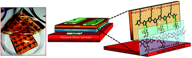
Apart from the development of new dielectric and semiconductor materials, the semiconductor–dielectric interface study is also very important for the optimum performance of organic thin film transistors (OTFTs). Herein, we have reported the detailed synthesis of a whole new family of dielectric materials which are 1,3,5,7-tetrabromoadamantane; 1,3,5,7-tetrachloroadamanatane; 1,3,5,7-tetraiodoadamantane and 1,3,5,7-tetrauraciladamantane (AdUr4). The unique ability of these molecules to undergo supramolecular thin film formation at low temperature, was analysed for their potential use as an insulator in organic electronic devices. Owing to the good leakage current density property shown by AdUr4 dielectric material it was further employed as a gate dielectric in regioregular poly(3-hexylthiophene), (P3HT) based OTFT. This OTFT device which was fabricated on a flexible PI plastic substrate has shown a good on/off current ratio (e.g., 2.18 × 10⁴) and high mobility (e.g., 0.15 cm2 V−1 s−1). The semiconductor–dielectric interface study, has revealed that the AdUr4 gate dielectric layer has guided the P3HT molecular chain domains to undergo edge-on orientation, which is the charge transport direction in OTFTs. In this process, the grazing incidence X-ray diffraction (GI-XRD) analysis and AFM study was also employed.


1. Introduction

Organic thin film transistors (OTFTs) have been emerging as a new class of organic electronic devices, with a potential to replace the traditional silicon based transistors.1 They are expected to play a major role in future for the development of low cost electronic devices which will be tough, light weight and flexible.2 They have been the focus of research for the development of flexible electronics because of their cost-effective production, solution based processability and compatibility with variety of flexible substrates.3 Instead of so much merits associated with them, there are lot of challenges needs to be met before their commercialization for practical uses such as in the field of displays, sensors, invertors and radio frequency identification tags.4 The major hurdle coming in the commercialization of OTFTs is mainly due to their low output current and high operating voltage, as resulting from low charge carrier mobility of the active semiconducting layer employed respectively in them.5 In general, OTFTs are composed of three components namely an electrode, semiconducting layer and a dielectric insulating layer separating the active semiconducting material from a gate electrode. Thus the performance of OTFTs can be improved either by employing an organic semiconducting with better charge carrier mobility or with the use of dielectric material having low leakage current and high dielectric constant.6 In past various research groups have successfully achieved the high charge carrier mobility, μFE ≈ 10 cm2 V−1 s−1 by employing new organic semiconductor materials in OTFTs.7 However, the dielectric layer which also plays an important role in working of OTFTs, has been less explored as compared to semiconductor materials.8 The mobility and threshold voltage of OTFTs in the linear regime are related by the equation,9
 
image file: c4ra02077d-t1.tif(1)
where, IDS and VDS are the current and voltage bias between source and drain, respectively, VG denotes the gate voltage at which the current starts to rise. Further, W and L denotes the source–drain width and length, respectively; μFE is the field effect mobility; Ci is the capacitance per unit area of the insulator, and Vth is the threshold voltage. Thus, the proper choice of the dielectric material having low leakage current and high capacitance is essential for the low operating voltage OTFTs.10 The field induced charge carriers are confined to the thin region i.e. interface between semiconductor and dielectric layer in OTFTs.11 Hence, in combination with the development of new dielectric and semiconductor materials, the semiconductor–dielectric interface study is also pivotal for the optimum performance of OTFTs.12 Kim et al. have also reported,12a the effect of dielectric surface modification on the field-effect mobility of regioregular poly(3-hexylthiophene) (P3HT) based transistor. When the silicon dioxide SiO2 insulator substrate was modified with –OH terminated self-assembled monolayers (SAM), μFE was 0.08 cm2 V−1 s−1. However, upon SiO2 surface modification with –NH2 terminated SAM, the mobility increased by several orders of magnitude of 0.28 cm2 V−1 s−1 for the same P3HT semiconductor. This was due to the difference in orientation (perpendicular and parallel) of P3HT chains with respect to the modified SiO2 insulator substrate which lead to the difference in behaviour of device performance. Recently, Jenn-Chang Hwang et al. have reported13 the use of silk fibroin as a dielectric on the flexible poly(ethylene terephthalate) (PET) plastic substrate for the fabrication of pentacene OTFTs. The planner structure of the silk fibroin dielectric has allowed the pentacene molecules to self-assemble in the planner form which resulted in a very high μFE value of 23.2 cm2 V−1 s−1 in the saturation regime and a low operating voltage of −3 V. Hence, the proper choice of dielectric material with a good compatibility with the active semiconducting layer is also essential for the optimum performance of OTFTs.

Organic and polymeric materials have been extensively explored in recent years for their potential use as a gate dielectric in OTFTs. Nowadays, they are widely pursued over traditional SiO2 dielectric because of their low cost and their ability to form high quality thin films from them can be prepared by simple processing methods. These are spin coating, ink-jet printing and sol–gel process.14 Some of the most extensively explored polymers in this field are poly(methyl methacrylate) (PMMA), poly(styrene) (PS), poly(4-vinyl phenol) (PVP), poly(acrylic acid) (PAA), and poly(perfluorobutenyl vinyl ether) (CYTOP).15 These polymer gate dielectrics are known to have low leakage current which leads to the performance enhancement of OTFTs. However, due to their solubility in common organic solvents these polymer dielectrics get washed away during the deposition of organic semiconducting material by dip coating or spin coating methods.16 Some research groups have achieved the dielectric thin film of thickness <50 nm with high breakdown voltages by thermally crosslinking of the gate dielectric material.17 However, the curing temperature as needed for this process is higher than the glass transition temperature of flexible substrate.18 This leads to the poor performance of device. Therefore, there is a strong desire to design new organic dielectric materials which should be processable into thin film at low temperature from their solution in specific solvents.

Diamond is also a good insulator material,19 however its high cost, restricts its use as a gate dielectric in low cost OTFTs. On the other hand, the adamantane, (chemical formula C(4n+6)H(4n+12), where n = 0, 1, 2, 3…), which is the smallest cage structure of diamond, is cheap and can be easily obtained from oil and natural gas condensates after purification.20 This structurally rigid, thermally stable (pyrolysis temperature >660 °C) and easy to be chemically modified21 diamondoid molecule has recently been reviewed by Schwertfeger et al.22 The spatial arrangement of carbon atoms in adamantane is similar to that in diamond lattice.23 It has been broadly studied for its numerous applications in biology and chemistry.24

Motivated by so much merits associated with adamantane, we modified adamantane surface structure, chemically to synthesize its four derivatives namely; 1,3,5,7-tetrabromoadamantane (AdBr4); 1,3,5,7-tetrachloroadamanatane (AdCl4); 1,3,5,7-tetraiodoadamantane (AdI4) and 1,3,5,7-tetrauraciladamantane (AdUr4). The solution of these functionalized molecules has the ability to undergo smooth thin film formation at low temperature through supramolecular self-assembly (STF) (Scheme 1). The halogen–halogen interactions, van der Waals force of attractions and electrostatic force of attractions have played an important role in supramolecular polymeric thin films formation of AdBr4, AdCl4, AdI4. This unique ability of these small nanodiamond molecules to undergo thin film formation, with network structure similar to that of diamond lattice has prompted our group to explore their potential application as an insulator in organic electronics. This was analysed by employing these materials as insulating layer in MIM devices, as fabricated on flexible polyimide (PI) plastic substrate. The scanning electron microscope (SEM) study was employed to study morphology of organic dielectric thin films and further its effect was explored on MIM device performances as based on them. The difference in morphology of AdBr4, AdCl4, AdI4 STF has prevailed because of the different type of intermolecular forces involved in their formation. This was determinant in MIM device performance based on them. To further explore the effect of intermolecular forces on dielectric STF and its subsequent effect on the electrical performance of device we synthesised another unique derivative of adamantane, i.e. AdUr4. The uracil substituents on the surface of AdUr4 molecules has allowed them to adsorb on the gold coated flexible PI plastic substrate. Moreover, with Fourier transform infrared (FTIR) spectroscopy, it has been found that these AdUr4 molecules have undergone lateral interaction with each other through uracil–uracil (U⋯U) intermolecular hydrogen bonding that has led to the formation of their STF. Because of this the MIM devices as fabricated from AdUr4 STF showed better insulator properties as compared to that of AdBr4, AdCl4, AdI4 STF. The thermal stability of AdUr4 STF based MIM devices, was further analysed by heating them to various temperature and then measuring the leakage current at that corresponding temperature. The variable temperature FTIR spectroscopy was performed to find out the effect of heat on intermolecular hydrogen bonding involved in AdUr4 dielectric thin film. After this detailed analysis study of AdUr4 dielectric thin film, we employed it as a gate dielectric material in the P3HT based OTFTs with bottom gate and top contact. Through semiconductor–dielectric interface study, it has been found, that the unique rigid structure of AdUr4 has guided the regioregular P3HT chain domains to crystallize in edge-on orientation. The GI-XRD and atomic force microscopy study (AFM) was performed to successfully explore this phenomenon. The edge-on conformation has increased the charge carrier transfer to in-plane direction of P3HT chains which has led to the success of AdUr4 as a gate dielectric in P3HT based OTFTs with good on/off current ratio.


image file: c4ra02077d-s1.tif
Scheme 1 Schematic representation of the AdUr4 insulator supramolecular thin film formation on flexible PI plastic substrate: (a) flexible PI coated with Au/Cr layer is placed on a rigid support (solid block) in a beaker containing the solvent (THF) (b) injecting the drops of AdUr4 solution on this PI plastic substrate after 3–4 hours (c) the small rigid AdUr4 molecules self-assemble through U⋯U intermolecular hydrogen bonding into the form of a thin film. This last process takes 5–6 hours.

2. Experimental section

2.1 Reagents and materials

1-Bromoadamantane (99%), bromine (99.5%) and iodomethane was procured from Sigma Aldrich and used as received. Aluminum chloride and aluminum bromide anhydrous, powder of 99.999% trace metal basis was supplied by Alfa Aesar. The dichloromethane, chloroform and tetrahydrofuran (THF) obtained from Alfa Aesar were dried and distilled from sodium/benzophenone prior to their use. Chromium shots (Cr, 99.999%, Admat Inc.) 3–5 mm in size, aluminium shots (Al, 99.999%, Admat Inc.) 3–5 mm in size, and gold shots (Au, 99.999%, Admat Inc.) 1–2 mm in size, were purchased from Gredmann Taiwan Ltd. The organic semiconductor regioregular poly(3-hexylthiophene) (P3HT catalog number 698997 electronic grade, purchased from Aldrich, average molecular weight Mn 54[thin space (1/6-em)]000–75[thin space (1/6-em)]000, >98% head-to-tail regioregular) was adopted for this research. DuPont Kapton Polyimide film, 38 μm in thickness and from PV9100 series was used as substrate to fabricate the device.25 All other reagents and solvents were obtained from commercial suppliers and used as such, unless specified. It should be noted that all experiments were performed under dry nitrogen atmosphere and in standard fume hood.

2.2 Dielectric thin film preparation and fabrication of the MIM and OTFT devices

Scheme 1 presents the general method26 for the preparation of the respective dielectric thin films of AdBr4, AdCl4, AdI4, and AdUr4. In a typical thin film preparation experiment AdUr4 (0.05 mg) was dissolved in (10 mL) of THF under static conditions at 50 °C for 30 minutes. It was filtered with micro-syringe before drop casting on PI substrate. The dielectric thin film from tetrahedral molecules of adamantane derivatives were produced by their slowly self-assembling from a solution (0.05 mg mL−1) under a certain solvent pressure in a closed jar, as depicted in Scheme 1. It should be noted, that the solvent in the bottom of the jar was very crucial for the formation of well-defined smooth thin film from adamantane derivatives, which could play two important roles: (1) slow evaporation of the solvent guaranteed the small tetrahedral molecules had sufficient time to adjust themselves and come closer together with strong intermolecular interactions so that they can further self-assemble into smooth thin film on the substrate; (2) certain solvent vapour pressure in the upper space of the jar could guarantee the free movement of these molecules and then induced them to assemble together leading to the growth of polymer like film on the substrate. Apart from AdUr4 which have good solubility in THF the other halogen derivatives of adamantane as reported here, have good solubility in all organic solvents such as toluene, chloroform, chlorobenzene. However, the good solubility of all adamantane derivatives in THF and low vapor pressure of THF has prompted us to finally choose THF as a solvent of choice for the respective STF preparation of all the adamantane derivatives in this work.

A DuPont Kapton plastic PI plastic substrate with a thickness of 38 μm was used as the flexible substrate for the fabrication of MIM capacitor and OTFT devices. The PI plastic substrate was ultrasonically cleaned using ethanol (Fluka; water content: <0.1%) for 30 min and then rinsed with DI water. A high-pressure stream of N2 gas was then used to remove the water and any remaining particles from the PI surface. After being cleaned, the PI plastic substrate was annealed at 200 °C for 1 h under vacuum to achieve relative thermal stability and to enhance the adhesion strength. Next, Cr (20 nm thick) and Au (80 nm thick) were sequentially deposited onto the PI plastic substrate using a thermal coater. The Cr layer was used as the adhesion layer between the PI plastic substrate and the Au thin film.27 Au was deposited as a gate electrode over the Cr layer on the PI plastic substrate. This PI was then placed in a jar containing the THF solvent and the jar was covered for 6–8 h to maintain a suitable vapour pressure inside it as shown in Scheme 1. Finally, the filtered THF solution of AdUr4 was drop casted over this PI plastic substrate using a syringe in such a way that it should cover the whole PI surface. After, the complete evaporation of solvent from the PI plastic substrate as evaporated; it was heated at 40 °C for 10 min to remove any solvent trapped inside the dielectric film, formed by self-assembly of molecules. At the end of this experiment, Al films with a thickness of 300 nm were patterned as the top electrode using a shadow mask and a thermal coater.

The electrical insulating properties of the halogen and uracil adamantane derivatives respective thin films have been optimized for OTFT on the PI plastic substrate. For OTFT device fabrication Cr and Au, which had thickness of 20 and 80 nm, respectively, were sequentially deposited through a shadow mask using a thermal coater to function as gate electrodes. Then, gate dielectric AdUr4 thin film was prepared on it, as described in Scheme 1. The P3HT film was then deposited as a channel layer using a spin casting method, at room temperature and annealed at 40 °C for 30 minutes. Finally, source (S) and drain (D) Al electrodes with a thickness of 100 nm were deposited onto the Al/P3HT/AdUr4/Au/Cr/PI through a shadow mask, which yielded the top-contact electrode OTFTs. The channel length (L) and width (W) were 82 μm and 2000 μm, respectively.

2.3 Thin film characterizations and electrical measurements

The surface morphology of the AdBr4, AdCl4, AdI4 and AdUr4 respective self-assembled thin films on the PI plastic substrate was evaluated using scanning electron microscope (SEM, JEOL). The thicknesses of these films were estimated by optical ellipsometry techniques. The surface morphology of the P3HT film that was spin casted over insulator substrate on the PI plastic substrate was evaluated using atomic force microscopy (AFM, Digital Instruments Nanoscope, D-5000) with a scan size of 2 μm × 2 μm and a scan rate of 1 Hz. The FTIR spectrum was recorded using the FTIR spectrometer (model 580, Perkin-Elmer) with a resolution of 4.00 cm−1. An infrared spectrum was recorded under nitrogen atmosphere in the range of 500–4000 cm−1 to determine the functional groups in the molecular structure. The samples were prepared on PI substrate (1 × 1 cm2) for FTIR measurement. Further, variable temperature FTIR experiments were performed on AdUr4 STF. The AdUr4 thin film was prepared on PI plastic substrate (1 × 1 cm2) by following the procedure as shown in Scheme 1. This PI plastic substrate was then in situ heated from 40–120 °C under nitrogen flow (20 mL min−1) in a FTIR instrument equipped with temperature controller function. Corresponding to each temperature, FTIR spectrums were recorded for this AdUr4 STF. The XRD pattern for the organic P3HT film was recorded using a Rigaku D/max-IIIB diffractometer with Cu Kα radiation (λ = 1.5406 Å). The sample for XRD study was prepared by spin casting the THF solution of P3HT on the AdUr4 dielectric STF with PI as the substrate.
MIM Capacitor. To investigate, the electrical characterization of all the four adamantane derivatives dielectric thin films, the capacitance–voltage (CV) and the leakage current–voltage (IV) were measured using a HP-4284A C–V analyser and Agilent-4156 probe station, respectively. The real part of the dielectric constant (k) was calculated using the following formula
 
image file: c4ra02077d-t2.tif(2)
in which C is capacitance, t is the thickness of the dielectric film (measured by ellipsometry technique), Am the capacitance area, and εo the permittivity of vacuum. The leakage current was measured in direct current on the capacitors in the range 0–100 V with a holding time of 100 ms (Agilent 4156). A quasi-static capacitance versus voltage curve was taken at a sweep rate of 0.25 V s−1 using a Keithley 595 quasi-static C–V meter. We examined an additional property for AdUr4 dielectric based MIM device, to check its stability against the temperature. This was done by heating the MIM device to various temperatures and measuring the leakage current at that respective temperature.
OTFT device. The electrical characteristics of the transistors were measured in a nitrogen glove box on an Agilent-4156 probe station. The transistor parameters, such as charge carrier mobility, were calculated using the standard formalism of field-effect transistors in the linear and saturation regimes respectively. The P3HT based OTFTs exhibits output characteristics with pinch off and current saturation. The electrical characteristics of the P3HT based OTFTs are very stable during operation. The μFE value in the linear region (μFE, lin) is obtained from the transfer characteristics using eqn (1). The Ci value for the P3HT thin film transistor was measured using MIM structure fabricated next to the P3HT based OTFT device.

3. Results and discussion

The adamantane, a tricyclic saturated hydrocarbon (tricyclo[3.3.1.1]decane) is the smallest “nanodiamond” molecule.26 Its bulky molecular volume, rigidity and highly symmetrical tetrahedral shape makes it an ideal building block for nanofabrication.21,24 Our research group have took the advantage of this unique rigid structure of adamantane for its application, as an insulator in flexible organic electronic devices, first in MIM devices and then finally in OTFTs. The ability of adamantane molecule to undergo substitution reaction readily at its 1,3,5,7 position allowed us to prepare its four derivatives.20e These are AdBr4, AdCl4, AdI4, AdUr4, and was synthesized by following the Scheme 2. The STF of these compounds were prepared on flexible PI plastic substrate, as illustrated in Scheme 1 for their application as an insulator in MIM and OTFTs devices. It has been found that the supramolecular interactions, has guided these individual small rigid molecules to self-assemble28 in form of their rigid and flexible thin films. The STF of AdBr4, AdCl4, AdI4 molecules have occurred through halogen–halogen interactions i.e. Br⋯Br, Cl⋯Cl, I⋯I respectively.29–31 However, the AdUr4 molecules have knitted up together in the form of STF through U⋯U intermolecular hydrogen bonding.32 The Fig. 1 shows that in AdUr4 STF each AdUr4 molecule is involved in intermolecular hydrogen bonding with nearby AdUr4 molecules.
image file: c4ra02077d-s2.tif
Scheme 2 Synthetic route27 of dielectric materials based on adamantane (AdBr4, AdCl4, AdI4, AdUr4).

image file: c4ra02077d-f1.tif
Fig. 1 U⋯U intermolecular hydrogen bonding in AdUr4 molecules leading to their STF formation on the flexible PI plastic substrate. Free –NH (not involved in U⋯U intermolecular hydrogen bonding) are shown in yellow square box.

Furthermore, through FTIR study we also confirmed the presence of some free –NH (not involved in U⋯U intermolecular hydrogen bonding) of uracil in AdUr4 STF.

The difference in the respective STF of AdBr4, AdCl4, AdI4, AdUr4 is because of the different type of intermolecular forces involved in their formation. Due to this they have exhibited the different leakage current density, when employed as an insulating layer, in MIM devices. The IV characteristics of these respective MIM devices are shown in ESI (Fig. S5–S8). In Fig. 2, we have compared the leakage current density (capacitor area = 0.01 mm2) of these MIM devices and corresponding results has been shown in Table 1. The leakage current density of AdUr4, MIM device is 2.28 × 10⁻⁹ A cm−2 while the leakage current density of MIM devices based on AdCl4, AdBr4, AdI4 insulating materials are 1.74 × 10⁻⁶ A cm−2, 2.74 × 10⁻⁷ A cm−2 and 6.01 × 10⁻⁸ A cm−2 respectively. From this it can be concluded that the AdUr4 STF is an excellent insulator material followed by that of AdI4, AdBr4, and AdCl4. The good leakage current density of AdUr4 STF has motivated us to carry our further study to explore its potential use as a gate dielectric in OTFTs. Moreover, we have also measured the capacitance for these films and found the low dielectric constants, which are 2.1 for AdCl4, 2.09 for AdBr4 and 2.4 for AdI4. But, the better capacitance (209.0 nF cm−2) was measured for AdUr4 STF with better dielectric constant (2.6) than the other three films. Moreover, the thicknesses of AdCl4, AdBr4, AdI4 and AdUr4 films as estimated by ellipsometry are 10.2, 10.7, 11.5 and 11.0 nm respectively.

Table 1 Summary of all the characteristic properties of AdCl4, AdBr4, AdI4 and AdUr4 when incorporated as insulator layer in MIM devices
Dielectric material Thickness (nm) Dielectric constant Capacitance density (nF cm−2) Leakage current density (A cm−2)
AdCl4 10.2 2.1 182.0 1.74 × 10⁻⁶
AdBr4 10.7 2.09 172.0 2.74 × 10⁻⁷
AdI4 11.5 2.4 185.4 6.01 × 10⁻⁸
AdUr4 11.0 2.6 209.0 2.28 × 10⁻⁹


image file: c4ra02077d-f2.tif
Fig. 2 Comparison of leakage current behaviour of AdCl4, AdBr4, AdI4 and AdUr4.

It has been found that the difference in morphology of STF formed by these respective materials on PI plastic substrate has led to this difference in their electrical performance of MIM devices based on them.33 The AdBr4, AdCl4, AdI4 are well known to form plastic crystals through X⋯X interactions, as do other symmetrical adamantane derivatives. Pedireddi et al., have also reported30 that X⋯X (where X = Cl, Br, I) interactions can be represented as specific attractive forces. The attractive nature of X⋯X contacts depend on atomic polarization of respective halogen atoms, which varies as follow.34

Cl⋯Cl < Br⋯Br < I⋯I

The atomic size of chlorine, bromine and iodine atoms are 0.99 Å, 1.15 Å and 1.40 Å respectively.35 The I⋯I attractive contacts appeared because of electron cloud distortion of iodine atoms further leading to the formation of partial positive and negative charge on them. Thus, the I⋯I contacts that have prevailed in AdI4 STF are because of electrostatic forces of attractions among iodine atoms.30 Owing, to the larger atomic size, this distortion of electron clouds is much more pronounced in case of iodine atoms as compared to that of bromine and chlorine atoms. The X⋯X (where X = Cl, Br) that are present respectively in AdCl4, AdBr4 STF are because of van der Waals (vdW) interactions (attractive). Each molecule of AdBr4 has been interacted with the nearby two or three molecules of AdBr4 through these Br⋯Br vdW interactions.36 The vdW interactions are known to be of weaker strength as compared to that of electrostatic forces of attractions and intermolecular hydrogen bondings.37 Hence, due to weak intermolecular forces, AdBr4 molecules in its STF are not packed as closely as that of AdI4 molecules in AdI4 STF. Further, the smaller atomic size of chlorine atoms has resulted into more weaker X⋯X (X = Cl) vdW interactions among AdCl4 molecules resulting into the more loose packing of the AdCl4 molecules in their STF.31,34 The effect of this intermolecular interactions on molecular packing on surface morphology of STF was further analysed by SEM. It has been found that the AdI4 STF has smaller cracks followed by that of AdBr4 and AdCl4 (SEM images of these STF are shown in ESI S1–S3). Due to this difference in surface quality of AdX4 (X = Cl, Br, I) STF, the MIM devices based on them has showed the difference in their electrical performance.38 The halogen–halogen interactions are the weaker intermolecular forces of interactions as compared to that of intermolecular hydrogen bonds.39 Therefore, when AdUr4 STF were analysed by SEM, they appeared to be smooth with no pinholes or cracks, as shown in Fig. 3b. The SEM image in Fig. 3a shows the AdUr4 STF when prepared from its low concentration solution on PI plastic substrate (without following Scheme 1) appeared as cluster of AdUr4 molecules. In this case, the THF solution of AdUr4 was drop casted on PI plastic substrate and allowed to dry it in open atmosphere.


image file: c4ra02077d-f3.tif
Fig. 3 SEM image of (a) AdUr4 STF when prepared from THF solution of AdUr4 without following Scheme 1, (b) supramolecular thin film formed from THF solution of AdUr4 by following the Scheme 1.

We found that, for preparation of AdUr4 STF on PI plastic substrate by Scheme 1, has played a significant role in the formation of its smooth STF. In this method, the slow evaporation of solvent gives sufficient time to AdUr4 molecules to move closer to each other and then self-assemble in the form of their STF through U⋯U intermolecular hydrogen bonds.32 The AdUr4 molecules undergoes adsorption on gold coated surface layer (bottom electrode for MIM and OTFTs devices) on PI plastic substrate through uracil groups. This adsorption holds the individual AdUr4 molecules strongly against the gold coated PI plastic substrate.40 These molecules further interacts laterally with each other through intermolecular hydrogen bonding between uracil groups as shown in Fig. 1. In this process, –NH and –CO present in imide functional group of uracil acts as the donor and acceptor respectively, leading to the formation of rigid STF of AdUr4 on gold coated PI plastic substrate.

The role played by U⋯U intermolecular hydrogen bonds on stability of the AdUr4 STF was further characterized by variable temperature FTIR spectrometer.41 The AdUr4 STF on PI plastic substrate was heated to various temperatures and corresponding to each temperature the leakage current property of MIM capacitor device was analysed as shown in Fig. 4.


image file: c4ra02077d-f4.tif
Fig. 4 (a) IV characteristic property under different temperature of flexible 5 × 5 cm2 MIM device incorporated with AdUr4 insulator layer (b) corresponding variable temperature FTIR spectra of the AdUr4 STF as prepared on flexible PI plastic substrate.

It has been found that MIM devices, incorporated with AdUr4 STF as an insulator has shown good electrical performance up to 100 °C. This can be seen in terms of its high leakage current density, 3.30 × 10⁻³ A cm−2 at 120 °C as calculated from its IV characteristics curve in Fig. 4a. This has been attributed to breakage of U⋯U intermolecular hydrogen bonds at 120 °C, which has prevailed in AdUr4 STF. The variation in FT-IR spectra of AdUr4 thin film at 120 °C, in Fig. 4b shows this change. Hence, the excellent electrical performance shown by MIM devices incorporated with AdUr4 STF is due to the U⋯U intermolecular hydrogen bonds in them. The FTIR spectra of AdUr4 STF in Fig. 4b, shows the characteristic peaks corresponding to those of the free amide NH groups at 3475 cm−1 and that of –NH involved in U⋯U interactions at 3188 cm−1.41c Thus, the U⋯U intermolecular hydrogen bonds has played a significant role in success of the AdUr4 STF as new dielectric layer in flexible MIM device at high temperature. The success of AdUr4 STF based MIM devices, have prompted us to incorporate it as a gate dielectric layer in OTFTs.

In order to study the potential of the AdUr4 STF as a dielectric layer, we fabricated a P3HT based OTFTs with a bottom gate and top contact having a channel width of 2000 μm and a channel length of 82 μm (Fig. 5a). The Fig. 5b shows the photographic optical image of OTFTs as fabricated on flexible PI plastic substrate with its corresponding configuration shown in Fig. 5a. The Fig. 5c, shows the transfer characteristics for OTFTs. The Fig. 5d, presents the drain current–drain voltage (IDSVDS) output curve as obtained from our OTFT with a 11.0 nm thick AdUr4 dielectric layer, which is prepared according to Scheme 1. The device demonstrated, desirable OTFT characteristics at an operating voltage lower than −45 V. Maximum saturation current of 0.26 μA was achieved. The observed OTFT characteristics confirmed closely to conventional transistor models in both the linear and saturation regimes with IDS increasing linearly at low drainage voltage, and clear saturation behaviour at high drain voltage. According to the drain current–gate voltage (IDSVGS) transfer curve of Fig. 5c, the OTFT with the AdUr4 dielectric layer displayed an average field mobility of 0.15 cm2 V−1 s−1 at −45 V, threshold voltages (Vth) of −3 V, an on/off current ratio of 2.18 × 10⁴. Regioregular, P3HT is a material of choice for research OTFTs because of its high field effect mobility, stability, and solution processability. The orientation of P3HT molecular chains i.e. parallel (face-on structure) or perpendicular (edge-on structure) to the insulator substrate is an important phenomenon which need to be explored for the optimum performance of OTFTs. This phenomenon is much dependent on the chemical nature of the gate insulator material as it is the penultimate layer on which semiconducting layer is spin-casted. To study the structural ordering of spin coated films of P3HT on the insulator surface (AdUr4), we used synchrotron grazing-incidence X-ray diffraction (GI-XRD). The grazing incidence angle of 0.18° was employed and in order to isolate the scattering data from the P3HT polymer film only, the scan from a bare insulator substrate was used to remove background.42 The GI-XRD result is shown in Fig. 6a which demonstrates that the nanocrystalline regioregular P3HT molecular domains has mainly preferred to crystallize in edge-on orientation over the AdUr4 gate insulator as compared to their possible face-on orientation. These two different chain orientations of nanocrystalline regioregular P3HT domains with respect to the AdUr4 STF are evident from the different intensity distribution of the (100) reflections due to the lamellar layer structure (16.4 Å) and the (010) reflections due to interchain stacking (3.8 Å) through out-of-plane and in-plane geometric mode.12a,b The intense (100) reflections in the XRD spectra with respect to the (010) reflections shows that on AdUr4 STF the P3HT molecular chain domains has preferred to crystallize in edge on orientations, as shown in Fig. 6b. The GI-XRD has revealed this type of nanocrystalline structural order that has prevailed throughout the P3HT film, while the AFM observations was further done to provide images of the top surface. Fig. 6c, shows AFM topographic image of regioregular P3HT thin films on insulator substrate (AdUr4). The wormlike morphology of P3HT molecular chains in AFM image, has arisen because of their perpendicular orientations over insulator substrate (AdUr4).12a This edge on orientation of P3HT chains has led to their enhanced π–π stacking in the direction of charge transfer in OTFT.


image file: c4ra02077d-f5.tif
Fig. 5 (a) Schematic diagram of bottom gate OTFT device that features AdUr4 as a gate insulator and P3HT as a semiconducting layer (b) photograph of the OTFT devices on a 5 × 5 cm2 area on a flexible PI plastic substrate and plots for OTFT; (c) transfer characteristic (IDSVGS), when VDS = −2 V, and (d) output characteristic (IDSVDS), where VGS ranges from 0 to −15 V at −3 V step.

image file: c4ra02077d-f6.tif
Fig. 6 (a) Out of plane grazing-incidence angle X-ray diffraction intensities as a function of the scattering angle 2θ for regioregular P3HT thin films crystallized against insulator material AdUr4 on silicon wafer. (b) The insets show schematically the crystallography of the P3HT nano-crystallites with respect to the insulator material, AdUr4 (c) tapping phase mode AFM image of a regioregular P3HT film against the AdUr4 insulator on flexible PI substrates.

The presence of uracil moiety at the 1,3,5,7 position of the adamantane, in AdUr4 STF has played an important role in the appearance of edge on orientation of P3HT molecular chain domains. The AdUr4 molecules first undergoes adsorption on gold coated PI plastic substrate and then form AdUr4 STF through U⋯U intermolecular hydrogen bonds. The FTIR spectra of AdUr4 STF in Fig. 4b, shows that, their exist two type of –NH protons in uracil substructure. The one which are involved in intermolecular hydrogen bonding shows their characteristic peak at 3188 cm−1 while the other, free –NH protons which are not involved in intermolecular hydrogen bonding appears at 3475 cm−1. The free polar –NH protons have undergone π–H interaction (attractive) with thienyl backbone of the regioregular P3HT molecular chains. However, the lone pair of electrons on other type of (–NH)˙˙ protons in AdUr4 STF were involved in repulsion force with the π-electron cloud of the P3HT molecular chains. Therefore, the P3HT molecular chain domains experiences two opposite force of interactions, over the AdUr4 gate insulator thin film. These two counter forces i.e. force of attraction and repulsion makes the regioregular P3HT molecular chains to pack into the edge-on orientation, i.e. perpendicular to the insulator substrate.12a,b

Fig. 7 shows this whole mechanism of formation of edge-on orientation of P3HT molecular chains over AdUr4 STF dielectric layer. Further, the adamantane is a rigid tetrahedral molecule21 hence during molecular packing of the AdUr4 molecules in the form of STF there may exist some voids in them. In these voids the hexane chains on the backbone of P3HT stucks, which further helps the regioregular P3HT molecular chains to crystallize in edge-on orientations. These all factors has led to the success of our P3HT based OTFT device as fabricated with new gate insulator layer material AdUr4.


image file: c4ra02077d-f7.tif
Fig. 7 Bottom gate flexible thin film transistor configuration with schematic representation of P3HT polymer chains undergoing edge-on orientation against the AdUr4 insulator surface.

4. Conclusion

The recent advances in flexible OTFTs have highlighted the use of low cost technology and materials to replace the most commonly used semiconductor and dielectric materials. We have successfully synthesized new dielectric materials AdCl4, AdBr4, AdI4 and AdUr4 through easy to follow synthesis process. Their potential to act as a dielectric material was analysed by fabrication of MIM devices respectively from them. The comparisons of IV characteristics study of these respective MIM devices have showed that AdUr4 is a better insulator material for plastic electronics. The ability of AdUr4 molecules to undergo supramolecular thin film formation through intermolecular hydrogen bonding has been successfully explored here. Its use as a gate electrode in electronic devices, through fabrication of a new and fully flexible P3HT, a p-type OTFT on the flexible PI plastic substrate has also been demonstrated in this work. This P3HT based OTFT device incorporated with AdUr4 as a gate electrode showed good on/off current ratio (2.18 × 10⁴) and high charge mobility (0.15 cm2 V−1 s−1). The detailed semiconductor–dielectric interface study, lead us to conclude that the P3HT molecular chain domains has undergone edge-on crystallization (perpendicular to the insulator substrate), i.e. the charge transport direction in OTFTs. This study has explored a new efficient pathway for development of flexible OTFTs to their full potential on commercial scale, by exploiting the self-assembling ability of small molecules into thin films as a dielectric material in them.

Acknowledgements

The authors are grateful to the National Device Laboratories for their support in the device fabrication, the National Science Council of Taiwan for financially supporting this research under the contract NSC 101-2113-M-009-MY3.

Notes and references

  1. (a) H. Sirringhaus, Adv. Mater., 2005, 17, 2411 CrossRef CAS; (b) R. A. Street, Adv. Mater., 2009, 21, 2007 CrossRef CAS; (c) G. Malliaras and R. H. Friend, Phys. Today, 2005, 58, 53 CrossRef CAS PubMed; (d) S. J. Kim and J. S. Lee, Nano Lett., 2010, 10, 2884 CrossRef CAS PubMed.
  2. (a) P. M. Beaujuge and J. M. Frechet, J. Am. Chem. Soc., 2011, 133, 20009 CrossRef CAS PubMed; (b) C. Wang, H. Dong, W. Hu, Y. Liu and D. Zhu, Chem. Rev., 2012, 112, 2208 CrossRef CAS PubMed; (c) V. C. Sundar, J. Zaumseil, V. Podzorov, E. Menard, R. L. Willett, T. Someya, M. E. Gershenson and J. A. Rogers, Science, 2004, 303, 1644 CrossRef CAS PubMed; (d) M. Kaltenbrunner, T. Sekitani, J. Reeder, T. Yokota, K. Kuribara, T. Tokuhara, M. Drack, R. Schwodiauer, I. Graz, S. Bauer-Gogonea, S. Bauer and T. Someya, Nature, 2013, 499, 458 CrossRef CAS PubMed.
  3. (a) E. J. Meijer, D. M. De Leeuw, S. Setayesh, E. Van Veenendaal, B. H. Huisman, P. W. M. Blom, J. C. Hummelen, U. Scherf and T. M. Klapwijk, Nat. Mater., 2003, 2, 678 CrossRef CAS PubMed; (b) H. U. Khan, M. E. Roberts, W. Knoll and Z. N. Bao, Chem. Mater., 2011, 23, 1946 CrossRef CAS; (c) T. Sekitani, U. Zschieschang, H. Klauk and T. Someya, Nat. Mater., 2010, 9, 1015 CrossRef CAS PubMed; (d) H. Sirringhaus, T. Kawase, R. H. Friend, T. Shimoda, M. Inbasekaran, W. Wu and P. E. Woo, Science, 2000, 290, 2123 CrossRef CAS.
  4. (a) K. Cherenack and L. van Pieterson, J. Appl. Phys., 2012, 112, 091301 CrossRef PubMed; (b) M. S. White, M. Kaltenbrunner, E. D. Głowacki, K. Gutnichenko, G. Kettlgruber, I. Graz, S. Aazou, C. Ulbricht, D. A. M. Egbe, M. C. Miron, Z. Major, M. C. Scharber, T. Sekitani, T. Someya, S. Bauer and N. S. Sariciftci, Nat. Photonics, 2013, 7, 811 CrossRef CAS; (c) X. H. Zhang Jr, W. J. Potscavage, S. K. Choi and B. Kippelen, Appl. Phys. Lett., 2009, 94, 043312 CrossRef PubMed; (d) R. Rotzoll, S. Mohapatra, V. Olariu, R. Wenz, M. Grigas and K. Dimmler, Appl. Phys. Lett., 2006, 88, 123502 CrossRef PubMed.
  5. (a) M. L. Chabinyc, F. Endicott, B. D. Vogt, D. M. DeLongchamp, E. K. Lin, Y. Wu, P. Liu and B. S. Ong, Appl. Phys. Lett., 2006, 88, 113514 CrossRef PubMed; (b) H. Sirringhaus, Adv. Mater., 2009, 21, 3859 CrossRef CAS; (c) A. Facchetti, Chem. Mater., 2011, 23, 733 CrossRef CAS.
  6. (a) X. Zhang, H. Bronstein, A. J. Kronemeijer, J. Smith, Y. Kim, R. J. Kline, L. J. Richter, T. D. Anthopoulos, H. Sirringhaus, K. Song, M. Heeney, W. Zhang, I. McCulloch and D. M. DeLongchamp, Nat. Commun., 2013, 4, 2238 Search PubMed; (b) C. Gu, W. Hu, J. Yao and H. Fu, Chem. Mater., 2013, 25, 2178 CrossRef CAS; (c) R. P. Ortiz, A. Facchetti and T. J. Marks, Chem. Rev., 2010, 110, 205 CrossRef CAS PubMed.
  7. (a) K.-J. Baeg, M. Caironi and Y.-Y. Noh, Adv. Mater., 2013, 25, 4210 CrossRef CAS PubMed; (b) J. Lee, J. Han, A.-R. Kim, Y. Kim, J. H. Oh and C. Yang, J. Am. Chem. Soc., 2012, 134, 20713 CrossRef CAS PubMed; (c) J. Li, Y. Zhao, H. S. Tan, Y. Guo, C.-A. Di, G. Yu, Y. Liu, M. Lin, S. H. Lim, Y. Zhou, H. Su and B. S. Ong, Sci. Rep., 2012, 2, 754 Search PubMed.
  8. I. McCulloch, Adv. Mater., 2013, 25, 1811 CrossRef CAS PubMed.
  9. S. M. Sze, Semiconductor Devices: Physics and Technology, Wiley, New York, 2nd edn, 1981 Search PubMed.
  10. (a) S. Wu, M. Shao, Q. Burlingame, X. Chen, M. Lin, K. Xiao and Q. M. Zhang, Appl. Phys. Lett., 2013, 102, 013301 CrossRef PubMed; (b) G. Lucovsky and V. Misra, Encyclopedia of Materials: Science and Technology, 2001, 2nd edn, p. 2070 Search PubMed; (c) C. Liu, Y. Xu, Y. Li, W. Scheideler and T. Minari, J. Phys. Chem. C, 2013, 117, 12337 CrossRef CAS.
  11. (a) A. Facchetti, M.-H. Yoon and T. J. Marks, Adv. Mater., 2005, 17, 1705 CrossRef CAS; (b) D. Natali and M. Caironi, Adv. Mater., 2012, 24, 1357 CrossRef CAS PubMed; (c) S. Alexander, A. S. Eggeman, S. Illig, A. Troisi, H. Sirringhaus and P. A. Midgley, Nat. Mater., 2013, 12, 1045–1049 CrossRef PubMed.
  12. (a) D. H. Kim, Y. D. Park, Y. Jang, H. Yang, Y. H. Kim, J. I. Han, D. G. Moon, S. Park, T. Chang, C. Chang, M. Joo, C. Y. Ryu and K. Cho, Adv. Funct. Mater., 2005, 15, 17 CrossRef; (b) H. Yang, T. J. Shin, L. Yang, K. Cho, C. Y. Ryu and Z. Bao, Adv. Funct. Mater., 2005, 15, 671 CrossRef CAS; (c) X. Xu, B. Liu, Y. Zou, Y. Guo, L. Li and Y. Liu, Adv. Funct. Mater., 2012, 22, 4139 CrossRef CAS; (d) H. Ma, H.-L. Yip, F. Huang and A. K.-Y. Jen, Adv. Funct. Mater., 2010, 20, 1371 CrossRef CAS.
  13. C.-H. Wang, C.-Y. Hsieh and J.-C. Hwang, Adv. Mater., 2011, 23, 1630 CrossRef CAS PubMed.
  14. (a) N. B. Ukah, J. Granstrom, R. R. S. Gari, G. M. King and S. Guha, Appl. Phys. Lett., 2011, 99, 243302 CrossRef PubMed; (b) J. Li, D. Liu, Q. Miaob and F. Feng Yan, J. Mater. Chem., 2012, 22, 15998 RSC; (c) M. Caironi, E. Gili and H. Sirringhaus, Ink-Jet Printing of Downscaled Organic Electronic Devices, in Organic Electronics II: More Materials and Applications, ed. H. Klauk, Wiley-VCH Verlag GmbH & Co. KGaA, Weinheim, Germany. 2012, ch. 9,  DOI:10.1002/9783527640218; (d) J. S. Meena, M.-C. Chu, Y.-C. Chang, C.-S. Wu, C.-C. Cheng, F.-C. Chang and F.-H. Ko, ACS Appl. Mater. Interfaces, 2012, 4, 3261 CrossRef CAS PubMed.
  15. (a) Y. Yun, C. Pearson and M. C. Petty, J. Appl. Phys., 2009, 105, 034508 CrossRef PubMed; (b) H. Yan, Z. Chen, Y. Zheng, C. Newman, J. R. Quinn, F. Dötz, M. Kastler and A. Facchetti, Nature, 2009, 457, 679 CrossRef CAS PubMed; (c) F. D. Angelis, S. Cipolloni, L. Mariucci and G. Ortunato, Appl. Phys. Lett., 2005, 86, 203505 CrossRef PubMed; (d) T.-W. Lee, Y. H. Byun, B. W. Koo, I.-N. Kang, Y.-Y. Lyu, C. H. Lee, L. S. Pu and S. Y. Lee, Adv. Mater., 2005, 17, 2180 CrossRef CAS.
  16. (a) J. Park, S. Y. Park, S. O. Shim, H. Kang and H. H. Lee, Appl. Phys. Lett., 2004, 85, 3283 CrossRef CAS PubMed; (b) S. H. Lim, J. Kim, S.-G. Lee and Y. S. Kim, Chem. Commun., 2010, 46, 3961 RSC.
  17. (a) Y. Fujisaki, Y. Nakajima, D. Kumaki, T. Yamamoto, S. Tokito, T. Kono, J. Nishida and Y. Yamashita, Appl. Phys. Lett., 2010, 97, 133303 CrossRef PubMed; (b) W. Xu, C. Guo and S. W. Rhee, J. Mater. Chem., 2012, 22, 6597 RSC; (c) T.-W. Lee, J. H. Shin, I.-N. Kang and S. Y. Lee, Adv. Mater., 2007, 19, 2702 CrossRef CAS.
  18. (a) H. Klauk, M. Halik, U. Zschieschang, G. Schmid, W. Radlik and W. J. Weber, J. Appl. Phys., 2002, 92, 5259 CrossRef CAS PubMed; (b) S. M. Pyo, M. Y. Lee, J. Jeon, J. H. Lee, M. H. Yi and J. S. Kim, Adv. Funct. Mater., 2005, 15, 619 CrossRef CAS; (c) A. A. Virkar, S. Mannsfeld, Z. Bao and N. Stingelin, Adv. Mater., 2010, 22, 3857 CrossRef CAS PubMed.
  19. (a) S. F. Adams and L. H. Caveny, AIP Conf. Proc., 1992, 246, 643 CrossRef CAS PubMed; (b) W. A. de Heer, J.-M. Bonard, K. Fauth, A. Châtelain, D. Ugarte and L. Forró, Adv. Mater., 1997, 9, 87 CrossRef CAS.
  20. (a) S. Landa and V. Machacek, Collect. Czech. Chem. Commun., 1933, 5, 1 CAS; (b) G. Guangli Wang, S. Shengbao Shi, P. Wang and T.-G. Wang, Fuel, 2013, 107, 706 CrossRef PubMed; (c) A. T. Balaban, J. Chem. Inf. Model., 2012, 52, 2856 CrossRef CAS PubMed; (d) B. J. Mair, M. Shamaiengar, N. C. Krouskop and F. D. Rossini, Anal. Chem., 1959, 31, 2082 CrossRef CAS; (e) L. J. Mathias, V. R. Reichert and A. V. G. Muirl, Chem. Mater., 1993, 5, 4 CrossRef CAS.
  21. (a) K. Morita, T. Hashimoto, M. Urushisaki and T. Sakaguchi, J. Polym. Sci., Part A: Polym. Chem., 2013, 51, 2445 CrossRef CAS; (b) A.-Y. Jee and M. Lee, Carbon, 2009, 47, 2546 CrossRef CAS PubMed; (c) E. M. Maya, I. García-Yoldi, A. E. Lozano, J. G. de la Campa and J. de Abajo, Macromolecules, 2011, 44, 2780 CrossRef CAS; (d) S. Zheng, J. Shi and R. Mateu, Chem. Mater., 2000, 12, 1814 CrossRef CAS; (e) L. J. Mathias, J. J. Jensen, V. T. Reichert, C. M. Lewis and G. L. Tullos, ACS Symp. Ser., 1996, 624, 197 CrossRef CAS PubMed.
  22. H. Schwertfeger, A. A. Fokin and P. R. Schreiner, Angew. Chem., Int. Ed., 2008, 47, 1022 CrossRef CAS PubMed.
  23. (a) R. C. Fort and P. R. Schleyer, Chem. Rev., 1964, 64, 277 CrossRef CAS; (b) J. E. Dahl, S. G. Liu and R. M. K. Carlson, Science, 2003, 299, 96 CrossRef CAS PubMed; (c) A. P. Marchand, Science, 2002, 299, 52 CrossRef PubMed.
  24. (a) S. D. Banister, S. M. Wilkinson, M. Longworth, J. Stuart, N. Apetz, K. English, L. Brooker, C. Goebe, D. E. Hibbs, M. Glass, M. Connor, L. S. McGregor and M. Kassiou, ACS Chem. Neurosci., 2013, 4, 1081 CrossRef CAS PubMed; (b) L. Wanka, I. Khalid and P. R. Schreiner, Chem. Rev., 2013, 113, 3516 CrossRef CAS PubMed; (c) J. Zhang, Z. Zhu, Y. Feng, H. Ishiwata, Y. Miyata, R. Kitaura, J. E. P. Dahl, R. M. K. Carlson, N. A. Fokina, P. R. Schreiner, D. Tománek and H. Shinohara, Angew. Chem., Int. Ed., 2013, 52, 3717 CrossRef CAS PubMed; (d) P.-L. E. Chu, L.-Y. Wang, S. Khatua, A. B. Kolomeisky, S. Link and J. M. Tour, ACS Nano, 2013, 7, 35 CrossRef CAS PubMed.
  25. (a) T. Strunskus, M. Grunze, G. Kochendoerfer and C. Wöll, Langmuir, 1996, 12, 2712 CrossRef CAS; (b) E. Lindner and R. P. Buck, Anal. Chem., 2000, 72, 336A CrossRef CAS.
  26. (a) P. R. Schreiner, N. A. Fokina, B. A. Tkachenko, H. Hausmann, M. Serafin, J. E. P. Dahl, S. Liu, R. M. K. Carlson and A. A. Fokin, J. Org. Chem., 2006, 71, 6709 CrossRef CAS PubMed; (b) M. Vörös, T. Demjén, T. Szilvási and A. Gali, Phys. Rev. Lett., 2012, 108, 267401 CrossRef; (c) A. Patzer, M. Schütz, T. Möller and O. Dopfer, Angew. Chem., 2012, 124, 5009 CrossRef.
  27. G. S. Lee, J. N. Bashara, G. Sabih, A. Oganesyan, G. Godjoian, H. M. Duong, E. R. Marinez and C. G. Gutiérrez, Org. Lett., 2004, 6, 1705 CrossRef CAS PubMed.
  28. (a) Z. Ding, R. Xing, Y. Sun, L. Zheng, X. Wang, J. Ding, L. Wanga and Y. Han, RSC Adv., 2013, 3, 8037 RSC; (b) J.-N. Tisserant, G. Wicht, O. F. Göbel, E. Bocek, G.-L. Bona, T. Geiger, R. Hany, R. Mezzenga, S. Partel, P. Schmid, W. B. Schweizer and J. Heier, ACS Nano, 2013, 7, 5506 CrossRef CAS PubMed; (c) A. Datar, R. Oitker and L. Zang, Surface-Assisted One Dimensional Self-Assembly of a Perylene Based Semiconductor Molecule, Chem. Commun., 2006, 1649 RSC; (d) Y. Su, J. Liu, L. Zheng, Z. Ding and Y. Han, RSC Adv., 2012, 2, 5779 RSC.
  29. (a) N. K. Nath, B. K. Saha and A. I. Nangia, New J. Chem., 2008, 32, 1693 RSC; (b) P. V. Gushchin, M. L. Kuznetsov, M. Haukka and V. Y. Kukushkin, J. Phys. Chem. A, 2013, 117, 2827 CrossRef CAS PubMed; (c) F. Zordan, L. Brammer and P. Sherwood, J. Am. Chem. Soc., 2005, 127, 5979 CrossRef CAS PubMed; (d) R. Gutzler, C. Fu, A. Dadvand, Y. Hua, J. M. MacLeod, F. Rosei and D. F. Perepichka, Nanoscale., 2012, 4, 5965 RSC.
  30. V. R. Pedireddi, D. S. Reddy, B. S. Goud, D. C. Craig, A. D. Rae and G. R. Desiraju, J. Chem. Soc., Perkin Trans. 2, 1994, 2, 2353 RSC.
  31. (a) M. V. Vener, A. V. Shishkina, A. A. Rykounov and V. G. Tsirelson, J. Phys. Chem. A, 2013, 117, 8459 CrossRef CAS PubMed; (b) R. S. Rowland and R. Taylor, J. Phys. Chem. A, 1996, 100, 7384 CrossRef CAS; (c) Y. V. Zefirov and A. V. Churakov, Russ. J. Inorg. Chem., 2000, 45, 1880 Search PubMed.
  32. (a) S. Irrera, A. Roldan, G. Portalone and N. H. De Leeuw, J. Phys. Chem. C, 2013, 117, 3949 CrossRef CAS; (b) S. Irrera and N. H. De Leeuw, Proc. R. Soc. A, 2011, 467, 1959 CrossRef CAS; (c) D. M. A. Smith, J. Smets and L. J. Adamowicz, J. Phys. Chem. A, 1999, 103, 5784 CrossRef CAS.
  33. (a) S. E. Fritz, T. W. Kelley and C. D. Frisbie, J. Phys. Chem. B, 2005, 109, 10574 CrossRef CAS PubMed; (b) H. Yang, C. Yang, S. H. Kim, M. Jang and C. E. Park, ACS Appl. Mater. Interfaces, 2010, 2, 391 CrossRef CAS PubMed.
  34. M. R. Scholfield, C. M. V. Zanden, M. Carter and P. S. Ho, Protein Sci., 2013, 22, 139 CrossRef CAS PubMed.
  35. J. C. Slater, J. Chem. Phys., 1964, 41, 3199 CrossRef CAS PubMed.
  36. (a) Y.-M. Zhang, C. Cao, Y. Y. Lu, Q. S. Zhang and T. B. Wei, Acta Crystallogr., Sect. E: Struct. Rep. Online, 2011, 67, o286 CAS; (b) P. R. Schreiner, L. V. Chernish, P. A. Gunchenko, E. Y. Tikhonchuk, H. H. Hausmann, M. Serafin, S. Schlecht, J. E. P. Dahl, R. M. K. Carlson and A. A. Fokin, Nature, 2011, 477, 308 CrossRef CAS PubMed; (c) W. Guo, E. Galoppini, R. Gilardi, G. I. Rydja and Y.-H. Chen, Cryst. Growth Des., 2001, 1, 231 CrossRef CAS; (d) M. F. Roll, J. W. Kampf and R. M. Laine, Cryst. Growth Des., 2011, 11, 4360–4367 CrossRef CAS.
  37. (a) J. D. Dunitz and A. Gavezzotti, Chem. Soc. Rev., 2009, 38, 2622 RSC; (b) J. S. Ovens, K. N. Truonga and D. B. Leznoff, Dalton Trans., 2012, 41, 1345 RSC; (c) G. Song, L. Zhang, C. He, D.-C. Fang, P. G. Whitten and H. Wang, Macromolecules, 2013, 46, 7423 CrossRef CAS.
  38. M. Kawamura, Y. Nakahara, M. Ohse, M. Kumei, K. Uno, H. Sakamoto, K. Kimura and I. Tanaka, Appl. Phys. Lett., 2012, 101, 053311 CrossRef PubMed.
  39. (a) P. Politzer and J. S. Murray, ChemPhysChem, 2013, 14, 278 CrossRef CAS PubMed; (b) H. Wang, X. R. Zhao and W. J. Jin, Phys. Chem. Chem. Phys., 2013, 15, 4320 RSC; (c) P. Metrangolo, H. Neukirch, T. Pilati and G. Resnati, Acc. Chem. Res., 2005, 38, 386 CrossRef CAS PubMed.
  40. (a) T. Dretschkow, A. S. Dakkouri and T. Wandlowski, Langmuir, 1997, 13, 2843 CrossRef CAS; (b) S. Irrera, G. Portalone and N. De Leeuw, Surf. Sci., 2013, 614, 20 CrossRef CAS PubMed; (c) S. Irrera, A. Roldan, G. Portalone and N. De Leeuw, J. Phys. Chem. C, 2013, 117, 3949 CrossRef CAS; (d) A. C. Papageorgiou, S. Fischer, J. Reichert, K. Diller, F. Blobner, F. Klappenberger, F. Allegretti, A. P. Seitsonen and J. V. Barth, ACS Nano, 2012, 6, 2477 CrossRef CAS PubMed; (e) H. B. de Aguiar, F. G. C. Cunha, F. C. Nart and P. B. Miranda, J. Phys. Chem. C, 2010, 114, 6663 CrossRef CAS.
  41. (a) M. S. Masouda, A. A. Ibrahim, E. A. Khalil and A. El-Marghany, Spectrochim. Acta, Part A, 2007, 67, 662 CrossRef PubMed; (b) S. Sivakova and J. S. Rowan, Chem. Soc. Rev., 2005, 34, 9 RSC; (c) C. C. Cheng, Y.-L. Chu, P.-H. Huang, Y.-C. Yen, C.-W. Chu, A. C.-M. Yang, F.-H. Ko, J.-K. Chen and F.-C. Chang, J. Mater. Chem., 2012, 22, 18127 RSC; (d) E. M. B. Janke and K. Weisz, J. Phys. Chem. B, 2013, 117, 4853 CrossRef PubMed.
  42. (a) J. Kim, E. Ryba and J. Bai, Polymer, 2003, 44, 6663 CrossRef CAS; (b) M. Birkholz, Thin Film Analysis by X-Ray Scattering, Wiley-VCH, Weinheim, Germany, 2006, p. 155 Search PubMed.

Footnote

Electronic supplementary information (ESI) available. See DOI: 10.1039/c4ra02077d

This journal is © The Royal Society of Chemistry 2014