Photovoltaic devices with a PEDOT:PSS:WOx hole transport layer†
Seung Joo Lee,
Abd. Rashid bin Mohd Yusoff and
Jin Jang*
Department of Information, Display and Advanced Display Research Center, Kyung Hee University, Dongdaemun-ku, Seoul 130-171, Republic of Korea. E-mail: jjang@khu.ac.kr; Fax: +82 2 961 0270; Tel: +82 2 961 0270
First published on 15th April 2014
Abstract
In this paper, we report a significantly improved fill factor (FF) of inverted poly(3-hexylthiophene) (P3HT) and indene-C60 bisadduct (ICBA) organic photovoltaic devices via surface modification. The influence of the poly(3,4-ethylenedioxythiophene):poly(styrene-sulfonate) (PEDOT:PSS) hole extraction layer (HEL) modified with tungsten oxide (WOx) on inverted organic photovoltaics is studied. It is demonstrated that the PEDOT:PSS:WOx modification leads to a remarkably high FF, while abruptly reducing the series resistance and at the same time increasing the shunt resistance. The efficiency increased from 3.93 to 5.37%, and it is demonstrated that PEDOT:PSS modified with WOx HEL is an attractive material for high performance organic photovoltaic devices.
Introduction
Organic photovoltaics (OPVs) have attracted huge attention as one of our future power sources due to their cost effectiveness, mechanical flexibility, non-toxicity and low weight.1–4 Basically, there are four main processes that occur, namely absorption of incident light to create an exciton; exciton diffusion towards the donor/acceptor interface and dissociation into a hole in the donor and an electron in the acceptor, which is generally known as a charge transfer exciton (CTE); CTE dissociation into free charge; and charge collection at the respective contacts. A few approaches can be introduced to improve the power conversion efficiency (PCE) of OPVs. The first approach is to synthesize new low bandgap materials so that wide range of wavelengths and probably the near infrared region can be covered.5,6 The second approach is to stack two or more single junction OPVs in one cell, which is known as a tandem cell.7,8 Today, with these two approaches, we have seen a rapid increment in PCE either in single junction or tandem OPVs. To the best of our knowledge, the best performance of 9.2% for single junction OPVs has been obtained by using a promising acceptor PTB7.9 On the other hand, due to the fact that the tandem cell is designed to have complementary absorption, it has already achieved 12% PCE.10 Even though we have seen a rapid improvement in the last few years, it is still relatively far behind as compared to its inorganic counterpart.10 Thus, to improve to performance of OPVs, an in-depth understanding of the short circuit current density (Jsc), open circuit voltage (Voc), and fill factor (FF) is important. Among these three factors, FF can be considered the least understood.In brief, voluminous literature has been published on field-dependent CTE dissociation. A strong field-dependent CTE dissociation rate changes the curvature of the photocurrent density (Jph) response and reduces the FF.11 The unbalanced charge transport also influences the FF.11 In the OPV case, the FF is usually distributed from 50% to 70%, and if the space charge limited current (SCLC) dominates, it is relatively impossible to obtain FF of more than 42%.12 A metal top contact can also affect the performance of OPVs as well as the FF. According to a previous study, a low work function metal top contact could pin the surface energy level and eliminate the dipole layer at the polymer/metal interface to enhance the FF.13 There is also a study on the series resistance (Rs), the shunt resistance (Rsh), the morphology, molecular packing, film thickness and interface between the electrode and the active layer.14 Moreover, previous studies showed that the FF decreases with an increase in the cell area due to the increased series resistance and acceleration of the recombination loss at low built-in junction potentials.15 Recently, there have been many reported studies on OPVs incorporated with various metal oxides.16–39
We have recently proposed a new surface modification material (PEDOT:PSS:WOx) that serves as a hole extraction layer when sandwiched between a photosensitive layer and a Ag top electrode resulting in improved FF, Jsc and Voc in inverted organic photovoltaic devices.40 To access the details of the origin of these improvements, we have performed a systematic electronic study of the photosensitive/PEDOT:PSS:WOx/Ag interface. We have successfully carried out the study based on a commonly used donor/acceptor (P3HT:ICBA) (Fig. 1). In this study, the relations among photoluminescence (PL), mobility, X-ray diffraction, transmission, and contact angle for FF inverted OPVs with different hole extraction layers were comprehensively studied.
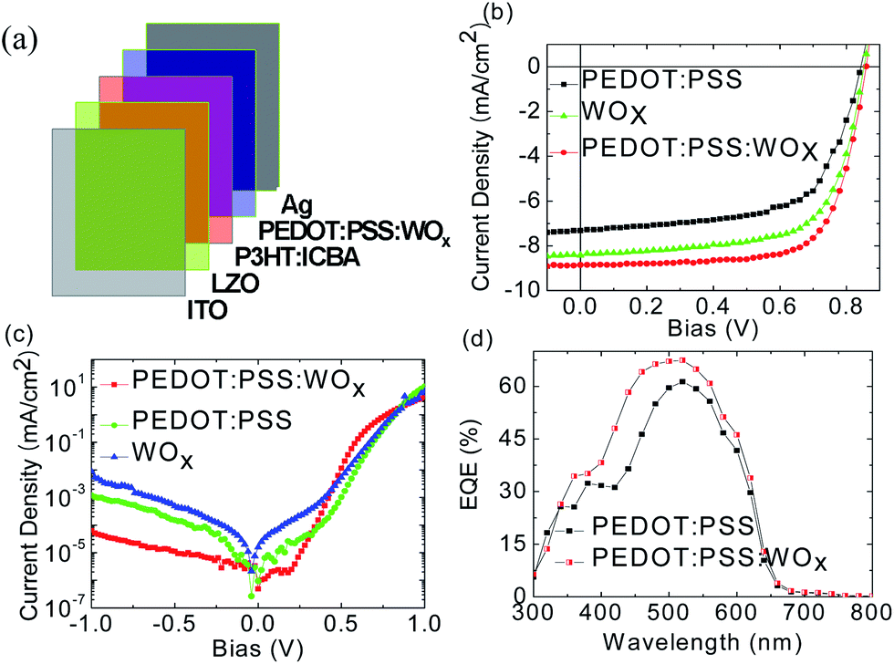 | ||
| Fig. 1 P3HT:ICBA-based single junction OPV performance with different hole extraction layers under simulated AM1.5G illumination. (a) Schematic structure of the studied OPVs, (b) J–V curves, (c) dark currents, and (d) external quantum efficiency. | ||
Results and discussion
Organic photovoltaic devices were fabricated using P3HT:ICBA blend bulk heterojunction active materials. P3HT:ICBA BHJ was dissolved in 1,2-dichlorobenzene and spin-coated onto lithium zinc oxide (LZO)-coated ITO substrates. A thin PEDOT:PSS or PEDOT:PSS:WOx hole extraction layer was then spin-coated onto the BHJ layer, followed by silver evaporation. Devices prepared using PEDOT:PSS:WOx showed the highest FF, and to the best of our knowledge, this is among the highest FFs ever reported in the literature for the P3HT:ICBA BHJ system.41–43 There are also a few reported works where the FF has exceeded 80%.44 The OPVs were measured under AM1.5G illumination, and the photovoltaic parameters are tabulated in Table 1. The reason why we used Al and Ag is to compare between reactive and less reactive metals. In addition, Ag is a low work function electrode, and based on many reported works, using Ag as the top electrode yielded higher efficiency as compared to using Al (top electrode).| HTL | Ade. | Jsc (mA cm−2) | Voc (V) | FF (%) | PCE (%) | Rs (Ω cm2) | Rsh (kΩ cm2) |
|---|---|---|---|---|---|---|---|
| a HTL = hole transport layer; Ade. = anode; P = PEDOT:PSS. | |||||||
| P:WOx | Ag | 8.91 | 0.86 | 71.00 | 5.37 | 1.20 | 1.05 |
| P | Ag | 7.32 | 0.84 | 63.61 | 3.93 | 12.00 | 2.31 |
| P:WOx | Al | 7.45 | 0.88 | 64.70 | 4.22 | 9.11 | 3.11 |
| WOx | Ag | 8.42 | 0.85 | 66.33 | 4.77 | 3.21 | 1.83 |
Fig. 1a shows our fabricated high FF inverted OPVs using Ag as the top electrode, and the current density–voltage (J–V) characteristics are shown in Fig. 1b. PEDOT:PSS and PEDOT:PSS:WOx devices showed reasonable Voc of 0.84 and 0.86 V, respectively. The PEDOT:PSS device demonstrated a Jsc value of 7.32 mA cm−2, whereas the PEDOT:PSS:WOx device showed a Jsc value of 8.91 mA cm−2. The Rs value is 12 and 1.2 Ω cm2 and the Rsh value is 1.05 and 2.31 kΩ cm2 for PEDOT:PSS and PEDOT:PSS:WOx, respectively. Moreover, the cell performance with various hole extraction layers was also studied under the dark condition. Fig. 1c depicts the dark J–V characteristics of the same organic photovoltaic device. A device fabricated with a PEDOT:PSS hole extraction layer demonstrates a remarkably higher dark current under revised bias as compared to the device fabricated with the PEDOT:PSS:WOx hole extraction layer corresponding to a high Rsh. The PEDOT:PSS:WOx surface modification device also demonstrates a low dark current density at a high forward bias in which it indicates a low series resistance. These high Rsh and low Rs values demonstrated by the device with the PEDOT:PSS:WOx modified surface corresponds to the highest rectification ratio. The low dark current density in the device with PEDOT:PSS:WOx also shows the effective blocking of misdirected charges. It is worth noting that PEDOT:PSS:WOx with the Al top electrode has a low FF as compared to PEDOT:PSS:WOx with the Ag electrode. Higher Jsc and FF values in the device utilizing Ag as the top electrode correspond to higher Rs and Rsh. In addition, we also fabricated OPV with only WOx as HTL, but the performance is not really convincing; Jsc = 8.42 mA cm−2, FF = 66.33%, and Voc = 0.85 V along with 4.77% PCE.
The fill factor (FF) values were 63.61 and 71% for PEDOT:PSS and PEDOT:PSS:WOx-based devices, respectively. As a result, the PCEs were 3.93% and 5.37% for PEDOT:PSS and PEDOT:PSS:WOx-based devices, respectively. External quantum efficiency (EQE) spectra are also shown in Fig. 1d. A high EQE response of greater than 50% over the range of 400–550 nm was observed for both OPVs. The EQEs were higher for the PEDOT:PSS:WOx device in the 550–800 nm range, partly because the PEDOT:PSS:WOx hole extraction layer has a higher light absorption at long wavelengths (Fig. 1), which is consistent with the higher Jsc values in the PEDOT:PSS:WOx device. The integrated EQE values for PEDOT:PSS and PEDOT:PSS:WOx were 7.22 and 8.62 mA cm−2, respectively. One may see some suppression of the dark current with the PEDOT:PSS:WOx hole extraction layer, where the efficiency increased because the FF is substantially increased due to the decreased Rs. Thus, a double hole extraction layer as the surface modifier is an interesting method of investigating whether each hole extraction layer acting alone is sufficient to block electrons.
To understand the reasons for the higher FF and Jsc in the PEDOT:PSS:WOx device as compared to the PEDOT:PSS device more specifically, we investigated the film morphology, exciton separation, carrier mobility, X-ray diffraction, transmittance, and water contact angle in the PEDOT:PSS and PEDOT:PSS:WOx blend films.
First, the film morphology was examined using atomic force microscopy (AFM) and scanning force microscopy (SEM). AFM images of both blend films, displayed in Fig. 2a and b, demonstrated smooth surfaces and the roughness of the PEDOT:PSS film (rms = 3.03 nm) was slightly lower than that of the PEDOT:PSS:WOx film (rms = 3.85 nm). SEM images of both layers are depicted in Fig. 2c and d.
 | ||
| Fig. 2 Atomic force microscopy and scanning electron microscopy images of (a and c) P3HT:ICBA/PEDOT:PSS and (b and d) P3HT:ICBA/PEDOT:PSS:WOx. All thin films were observed to possess very low surface roughness values of 3.03 nm (for PEDOT:PSS) and 3.85 nm (for PEDOT:PSS:WOx). | ||
The large FF value and slight Voc enhancement in this study result from the incorporation of the PEDOT:PSS:WOx hole extraction layer and both the enhancements show the combined modest electron blocking characteristics of PEDOT:PSS along with the superior electron blocking of WOx. Basically, good Rs along with large Rsh leads to better FF. Carrier mobilities were measured to estimate the ability of hole extraction. The hole mobilities of the PEDOT:PSS or the PEDOT:PSS:WOx blends were measured via the space charge limited current (SCLC) method using hole-only devices (ITO/PEDOT:PSS/P3HT:ICBA/Au). The JL3–V characteristics of the PEDOT:PSS and the PEDOT:PSS:WOx films are shown in Fig. 3.
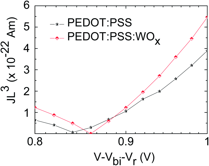 | ||
| Fig. 3 JL3 vs. (V − Vbi − Vr) plots for PEDOT:PSS and PEDOT:PSS:WOx layers. | ||
For all films, a slope of 2 in the log![[thin space (1/6-em)]](https://www.rsc.org/images/entities/char_2009.gif) JL3–logV plot was observed. The hole mobilities of the PEDOT:PSS and PEDOT:PSS:WOx layers were estimated to be 5 × 10⁻⁸ and 6 × 10⁻⁸ cm2 V−1 s−1, respectively. The considerable low mobility in the PEDOT:PSS film may result from the less uniform, more aggregated morphology as mentioned before. From this carrier mobility measurement, we concluded that the higher hole mobility of the PEDOT:PSS:WOx blends contributed to the higher Jsc values. The PEDOT:PSS and PEDOT:PSS:WOx layers were also analyzed by X-ray diffraction (XRD) studies. Fig. S1† shows the XRD patterns of PEDOT:PSS and PEDOT:PSS:WOx layers. All film XRD results were similar and showed amorphous features with a broad peak around 23°.
JL3–logV plot was observed. The hole mobilities of the PEDOT:PSS and PEDOT:PSS:WOx layers were estimated to be 5 × 10⁻⁸ and 6 × 10⁻⁸ cm2 V−1 s−1, respectively. The considerable low mobility in the PEDOT:PSS film may result from the less uniform, more aggregated morphology as mentioned before. From this carrier mobility measurement, we concluded that the higher hole mobility of the PEDOT:PSS:WOx blends contributed to the higher Jsc values. The PEDOT:PSS and PEDOT:PSS:WOx layers were also analyzed by X-ray diffraction (XRD) studies. Fig. S1† shows the XRD patterns of PEDOT:PSS and PEDOT:PSS:WOx layers. All film XRD results were similar and showed amorphous features with a broad peak around 23°.
Mixing PEDOT:PSS and WOx as the hole extraction layer most likely blocks almost all misdirected electrons and thus reduces recombination at the electrode and can increase Jsc. This is likely because of the decreased Rs and increased Rsh resulting from the increased electron blocking character of a PEDOT:PSS:WOx double hole extraction layer. Hau and co-workers45 reported that the Jsc enhancement can be attributed to an improved surface morphology of the photosensitive layer, induced by the surface energy modification at the interface. The Jsc of the PEDOT:PSS:WOx based devices is observed to be significantly higher than the Jsc of the PEDOT:PSS reference devices. To investigate the origin of the difference, we measured the transmission of the hole extraction layers (Fig. S2†). The PEDOT:PSS:WOx layer shows an approximately 10% lower transmission over wavelengths above 356 nm than the PEDOT:PSS layer. Below 470 nm, the gap in the transmission is further decreased. The EQEs of the PEDOT:PSS:WOx based devices are comparable for all wavelengths above 356 nm. Overall, the EQE measurements show that the Jsc is 20% higher for the PEDOT:PSS:WOx device than for the PEDOT:PSS device, which is in good agreement with the J–V measurements. This similarity of the transmission and EQE measurements might be explained by the longer pathway and therefore better absorption of the forward scattered light of the PEDOT:PSS:WOx material.
To support our abovementioned hypothesis, photoluminescence (PL) was measured to investigate the charge transport efficiency. The excitation light (λext = 325 nm) incident on the PEDOT:PSS and PEDOT:PSS:WOx layers yielded PL in the range of 325–575 nm.
Fig. 4 shows the PL spectra of both layers spin-coated from CB solutions onto the P3HT:ICBA layer. Both the PEDOT:PSS and PEDOT:PSS:WOx layers displayed PL with a peak around 380 nm. Blending PEDOT:PSS with WOx significantly quenched PL. This effective PL quenching suggested an effective interfacial charge transfer process. This suggests that additional pathways for the disappearance of the charge carriers exist due to the interactions between the excited PEDOT:PSS and WOx. This demonstrates that the PEDOT:PSS:WOx layer has a lower recombination rate of electrons and holes under UV light illumination, which is due to the fact that the electrons are excited by the HOMO to the LUMO level of PEDOT:PSS and later transfer to WOx, thus preventing a direct recombination of electrons and holes. WOx is regarded as a good hole extraction and electron blocking material to completely prevent the electron–hole pair recombination. That is, the miscibility between PEDOT:PSS and WOx is an important factor for efficient charge transport. In conclusion, morphology and PL quenching studies revealed that the PEDOT:PSS:WOx layer has more favourable features for higher Jsc.
 | ||
| Fig. 4 Photoluminescence spectra of PEDOT:PSS and PEDOT:PSS:WOx layers spin-coated from solution on the P3HT:ICBA layer. | ||
Finally, the water contact angle indicates that the surface energy of PEDOT:PSS has been modified, which is caused by WOx. As shown in Fig. S3,† the water contact angle measurement shows that the surface of P3HT:ICBA/PEDOT:PSS:WOx (26°) is more hydrophobic than that of P3HT:ICBA/PEDOT:PSS (34°). These observations show that the smoother and more hydrophobic surface of the PEDOT:PSS:WOx layer improves the compatibility between the active layer and the PEDOT:PSS:WOx layer and induces a better contact between them.
Conclusions
Efficient inverted OPVs are demonstrated using solution processed PEDOT:PSS:WOx as the hole extraction layer. The application of PEDOT:PSS:WOx dominantly increases the FF up to over 70% as well as the Jsc of the OPVs. PEDOT:PSS:WOx based devices show better performance than the PEDOT:PSS references, along with superior PCE of 5.37%. It was found that the more balanced carrier transport in PEDOT:PSS:WOx corresponds to higher FF and the effective PL indicates the effectiveness of the interfacial charge transfer process, which accounts for the higher Jsc.Experimental section
WOx solution preparation
Ammonium metatungstate hydrate (H26N6O40W12H2) powder purchased from Sigma Aldrich was used without further purification. 1 mM of the precursor was added to 1 mM deionized water–2 M HCL. The mixed solution was heated for 1 h and prior to the usage, the mixed solution was filtered using a 0.45 μm hydrophilic filter to remove unwanted particles.PEDOT:PSS:WOx solution preparation
The obtained WOx solution was mixed with PEDOT:PSS solution in a 1:1 ratio.
Two types of inverted OPVs were designed, and their structures are as follows:
(i) ITO/LZO/P3HT:ICBA/PEDOT:PSS/Ag (reference).
(ii) ITO/LZO/P3HT:ICBA/PEDOT:PSS:WOx/Ag.
The ITO glass was cleaned by ultrasonic treatment in a detergent, deionized water, acetone, and isopropanol. The pre-cleaned ITO substrate was treated in an ultraviolet-ozone chamber (Ultraviolet Ozone Cleaner, Jetlight Company, USA) for 15 min. The lithium zinc oxide (LZO) cathode buffer layer was spin-coated at 700 rpm for 25 s on the ITO electrode.16 The LZO film was annealed in air at 300 °C for 10 min. One of the reasons that we adopted LZO (2 wt%) in this study is the fact that LZO outperforms other metal oxides such as ZnO and AZO. The substrate was transferred to a nitrogen-filled glove-box, and the photoactive blend layer was prepared by spin coating (700 rpm) a 1,2-dichlorobenzene solution of P3HT and ICBA (1:1 w/w, polymer concentration 20 mg mL−1) on the LZO-coated ITO electrode for 25 s and then baking it at 150 °C for 10 min. The thickness of the active layer was around 90 nm. The PEDOT:PSS:WOx solution was filtered through a 0.45 μm hydrophilic filter and spin-coated at 4000 rpm for 25 s on the P3HT:ICBA. Later, the PEDOT:PSS:WOx film was baked at 130 °C for 20 min in air. The thickness of the PEDOT:PSS:WOx film was ∼28 nm. Finally, the substrate was transferred to a vacuum chamber, and 100 nm of Ag was thermally deposited on the photoactive layer at a base pressure of 1 × 10⁻⁷ Torr. The active area of the device was 0.04 cm2. 44 devices were fabricated in this study to ensure their reproducibility with an average PCE of 5.37%. The best device demonstrated 5.44% PCE along with 71.12% FF (see Table S1†).
AFM imaging was carried out in air using a Digital Instrument Multimode instrument equipped with a nanoscope IIIa controller. The transmittances of PEDOT:PSS and PEDOT:PSS:WOx coated on ITO-glass substrates were recorded at room temperature with a SCINCO S4100 spectrophotometer. All measurements were performed at room temperature. The power conversion efficiencies of the inverted OPVs were measured under the illumination of AM1.5G simulated solar light (Oriel Model 91192) at 100 mW cm−2. The current density–voltage (J–V) characteristics were recorded with a Keithley 2410 source meter. The external EQE measurements were performed using an EQE system (Model 74000) obtained from Newport Oriel Instruments, USA, and a HAMAMATSU calibrated silicon cell photodiode was used as the reference diode. The wavelength was controlled at 300–800 nm with a monochromator. Scanning electron microscopy (SEM) was carried out using Hitachi S-4700. Photoluminescence (PL) intensity was obtained using a JASCO FP-6500 spectrofluorometer. The XRD spectrum was obtained in the grazing incidence 2θ scan mode using X'PERT PRO from PANalytical. The hole mobilities of the PEDOT:PSS and PEDOT:PSS:WOx layers were measured according to the space charge limited current (SCLC) method using hole-only devices composed of ITO/PEDOT:PSS or PEDOT:PSS:WOx/P3HT:ICBA/Au. The current density versus voltage (J–V) characteristics were recorded on a Keithley model 2400 source measuring unit. The SCLC behavior was analyzed using the Mott–Gurney equation:

Acknowledgements
This work was supported by the Human Resources Development program (No. 20134010200490) of the Korea Institute of Energy Technology Evaluation and Planning (KETEP) grant funded by the Korea government Ministry of Trade, Industry, and Energy.References
- J. Y. Kim, K. Lee, N. E. Coates, D. Moses, T. Q. Nguyen, M. Dante and A. J. Heeger, Science, 2007, 317, 222 CrossRef CAS PubMed.
- Y. Yang and F. Wudl, Adv. Mater., 2009, 21, 1401 CrossRef CAS.
- N. N. Wang, J. S. Yu, Y. Zang, J. Huang and Y. D. Jiang, Sol. Energy Mater. Sol. Cells, 2010, 94, 263 CrossRef CAS PubMed.
- J. Huang, J. S. Yu, Z. Q. Guan and Y. D. Jiang, Appl. Phys. Lett., 2010, 97, 143301 CrossRef PubMed.
- J. Peet, J. Y. Kim, N. E. Coates, W. L. Ma, D. Moses, A. J. Heeger and G. C. Bazan, Nat. Mater., 2007, 6, 497 CrossRef CAS PubMed.
- Y. Y. Liang, D. Q. Feng, Y. Wu, S. T. Tsai, G. Li, C. Ray and L. P. Yu, J. Am. Chem. Soc., 2009, 131, 7792 CrossRef CAS PubMed.
- S. Sista, Z. R. Hong, L. M. Chen and Y. Yang, Energy Environ. Sci., 2011, 4, 1606 CAS.
- S. C. Price, A. C. Stuart, L. Q. Yang, H. X. Zhou and W. You, J. Am. Chem. Soc., 2011, 133, 4625 CrossRef CAS PubMed.
- R. F. Service, Science, 2011, 332, 293 CrossRef CAS PubMed.
- K. M. Coakley and M. D. Mcgehee, Chem. Mater., 2004, 16, 4533 CrossRef CAS.
- D. Gupta, S. Muukhopadhyay and K. S. Narayan, Sol. Energy Mater. Sol. Cells, 2011, 94, 1309 CrossRef PubMed.
- V. D. Mihailetchi, J. Wildeman and P. W. M. Blom, Phys. Rev. Lett., 2005, 94, 126602 CrossRef CAS.
- D. Gupta, M. Bag and K. S. Narayan, Appl. Phys. Lett., 2008, 92, 093301 CrossRef PubMed.
- M. S. Kim, B. G. Kim and J. S. Kim, ACS Appl. Mater. Interfaces, 2009, 1, 1264 CAS.
- W. Jeong, J. Lee, S. Y. Park, J. W. Kang and J. J. Kim, Adv. Funct. Mater., 2011, 21, 343 CrossRef CAS.
- A. R. B. M. Yusoff, H. P. Kim and J. Jang, Sol. Energy Mater. Sol. Cells, 2013, 109, 63 CrossRef PubMed.
- M.-F. Xu, L.-S. Cui, X.-Z. Zhu, C.-H. Gao, X.-B. Shi, Z.-M. Jin, Z.-K. Wang and L.-S. Liao, Org. Electron., 2013, 14, 657 CrossRef CAS PubMed.
- S.-H. Lin, S. Lan, J.-Y. Sun and C.-F. Lin, Org. Electron., 2013, 14, 26 CrossRef CAS PubMed.
- G. Terán-Escobar, J. Pampel, J. M. Caicedo and M. Lira-Cantú, Energy Environ. Sci., 2013, 6, 3088 Search PubMed.
- P.-N. Yeh, T.-H. Jen, Y.-S. Cheng and S.-A. Chen, Sol. Energy Mater. Sol. Cells, 2014, 120, 728 CrossRef CAS PubMed.
- H. Yan, D. Li, C. He, Z. Wei, Y. Yang and Y. Li, Nanoscale, 2013, 5, 11649 RSC.
- I. Lange, J. Kniepert, P. Pingel, I. Dumsch, S. Allard, S. Janietz, U. Scherf and D. Neher, J. Phys. Chem. Lett., 2013, 4, 3865 CrossRef CAS.
- Y. Li, Chem.–Asian J., 2013, 8, 2316 CrossRef CAS PubMed.
- S. Ulum, N. Holmes, M. Barr, A. Kilcoyne, B. B. Gong, X. Zhou, W. Belcher and P. Dastoor, Nano Energy, 2013, 2, 897 CrossRef CAS PubMed.
- D. Gao, B. Djukic, W. Shi, C. R. Bridges, L. M. Kozycz and D. S. Seferos, ACS Appl. Mater. Interfaces, 2013, 5, 8038 CAS.
- T. Ameri, T. Heumüller, J. Min, N. Li, G. Matt, U. Scherf and C. J. Brabec, Energy Environ. Sci., 2013, 6, 1796 CAS.
- M. A. Faist, S. Shoaee, S. Tuladhar, G. F. A. Dibb, S. Foster, W. Gong, T. Kirchartz, D. D. C. Bradley, J. R. Durrant and J. Nelson, Adv. Energy Mater., 2013, 3, 744 CrossRef CAS.
- J. M. Lee, B.-H. Kwon, H. I. Park, H. Kim, M. G. Kim, J. S. Park, E. S. Kim, S. Yoo, D. Y. Jeon and S. O. Kim, Adv. Mater., 2013, 25, 2011 CrossRef CAS PubMed.
- C. Hsin-Yi, S. Lan, P.-C. Yang, S.-H. Lin, J.-Y. Sun and C.-F. Lin, Sol. Energy Mater. Sol. Cells, 2013, 113, 90 CrossRef CAS PubMed.
- F. Wang, L. Li, Q. Xu, D. Qian, S. Li and Z. Tan, Org. Electron., 2013, 14, 845 CrossRef CAS PubMed.
- T. E. Kang, H.-H. Cho, C.-H. Cho, K.-H. Kim, H. Kang, M. Lee, S. Lee, B. Kim, C. Im and B. J. Kim, ACS Appl. Mater. Interfaces, 2013, 5, 861 Search PubMed.
- H. P. Kim, A. R. B. M. Yusoff and J. Jang, Sol. Energy Mater. Sol. Cells, 2013, 108, 38 CrossRef CAS PubMed.
- F. Cheng, G. Fang, X. Fan, H. Huang, Q. Zheng, P. Qin, H. Lei and Y. Li, Sol. Energy Mater. Sol. Cells, 2013, 110, 63 CrossRef CAS PubMed.
- S.-H. Lin, S. Lan, J.-Y. Sun and C.-F. Lin, Org. Electron., 2013, 14, 26 CrossRef CAS PubMed.
- S. Singh, B. Pandit, G. Hukic-Markosian, T. P. Basel, Z. V. Vardeny, S. Li and D. Laird, J. Appl. Phys., 2012, 112, 123505 CrossRef PubMed.
- Y.-H. Lin, Y.-T. Tsai, C.-C. Wu, C.-H. Tsai, C.-H. Chiang, H.-F. Hsu, J.-J. Lee and C.-Y. Cheng, Org. Electron., 2012, 13, 2333 CrossRef CAS PubMed.
- L. N. S. A. Thummalakunta, C. H. Yong, K. Ananthanarayanan and J. Luther, Org. Electron., 2012, 13, 2008 CrossRef CAS PubMed.
- S.-H. Liao, Y.-L. Li, T.-H. Jen, Y.-S. Cheng and S.-A. Chen, J. Am. Chem. Soc., 2012, 134, 14271 CrossRef CAS PubMed.
- A. R. B. M. Yusoff, H. P. Kim and J. Jang, Nanoscale, 2014, 6, 1537 RSC.
- S. J. Lee, H. P. Kim, A. R. B. M. Yusoff and J. Jang, Sol. Energy Mater. Sol. Cells, 2013, 124, 238 Search PubMed.
- J. You, L. Dou, K. Yoshimura, T. Kato, K. Ohya, T. Moriarty, K. Emery, C.-C. Chen, J. Gao, G. Li and Y. Yang, Nat. Commun., 2013, 4, 1446 CrossRef PubMed.
- A. Bulusu, S. A. Paniagua, B. A. Macleod, A. K. Sigdel, J. J. Berry, D. C. Olson, S. R. Marder and S. Graham, Langmuir, 2013, 29, 3935 CrossRef CAS PubMed.
- Q. Xu, F. Wang, Z. Tan, L. Li, S. Li, X. Hou, G. Sun, X. Tu, J. Hou and Y. Li, ACS Appl. Mater. Interfaces, 2013, 5, 10658 CAS.
- X. Guo, N. Zhou, S. J. Luo, J. Smith, D. B. Tice, J. W. Hennek, R. P. Ortiz, J. T. L. Navarrete, S. Li, J. Strzalka, L. X. Chen, R. P. H. Chang, A. Facchetti and T. J. Marks, Nat. Photon., 2013, 7, 825 CrossRef CAS.
- S. K. Hau, H.-L. Yip, O. Acton, N. S. Baek, H. Ma and A. K. Jen, J. Mater. Chem., 2008, 18, 5113 RSC.
Footnote |
| † Electronic supplementary information (ESI) available: XRD patterns. See DOI: 10.1039/c4ra01580k |
| This journal is © The Royal Society of Chemistry 2014 |