DOI:
10.1039/C4RA01517G
(Paper)
RSC Adv., 2014,
4, 18493-18502
Polystyrene-block-poly(methylmethacrylate) composite material film as a gate dielectric for plastic thin-film transistor applications†
Received
21st February 2014
, Accepted 2nd April 2014
First published on 3rd April 2014
Abstract
We report a simple approach to fabricate an organic–inorganic hybrid gate insulator based n-type thin-film transistor (TFT) on a plastic polyimide (PI) sheet at room temperature using an appropriate composition of commercially available polymers and block copolymer surfactant. The composite material film namely; polystyrene-block-poly(methylmethacrylate) (PS-b-PMMA) is readily deposited as a gate dielectric with zinc oxide (ZnO) as a semiconductor layer. This new dielectric material film exhibits high surface energy, high air stability, very low leakage current density and better dielectric constant as compared to the conventional polymer dielectrics. This plastic ZnO–TFT combines the advantages of a high-mobility transparent inorganic semiconductor with an ultrathin high-capacitance and low-leakage PS-b-PMMA composite gate dielectric. Fourier transform infrared (FT-IR) spectrum analysis is used for the PS-b-PMMA film to confirm the presence of functional components in this composite material film. The contact angle measurements for three test liquids (e.g., distilled water, ethylene glycol and diiodomethane) reveal that the composite dielectric materials film is nearly hydrophobic and the calculated surface energy is 35.05 mJ m−2. The resulting TFT exhibits excellent operating characteristics at VDS = 10 V with a drain–source current on/off modulation ratio (Ion/Ioff) of 3.12 × 10⁶ and a carrier mobility of 2.48 cm2 V−1 s−1. Moreover in the bending mode and in a normal environment, the device remained undistorted and shows better reliability and performance, while the thickness of PS-b-PMMA is about 28 nm. The results have suggested a new and easy approach for achieving transparent and functionally bendable optoelectronics devices.
1. Introduction
The transistor is the most important invention of the 20th century and from the day of its invention it has spread into our daily lives as an invaluable element in innumerable electronic products. The future demand for next-generation mobile computing, communication and identification devices has increased markedly throughout the past decades and is expected to continue to increase throughout coming of the century. For diverse multiple functionalities, the electronics of ideal mobile devices must achieve light weight, low power consumption, low operating voltages (powered by household batteries) and compatibility with various substrates.1 In addition the desired features of optical transparency, mechanical ruggedness, environmental stability, eco-friendly and inexpensive room temperature (RT) as well large area fabrication must be matched to customers' needs.2 Silicon and other II/VI and III/V compound semiconductors based TFTs exhibit necessary features such as high carrier mobility and high breakdown field.3 But these TFTs are limited by relating to high temperature processing (>400 °C) and mechanical flexibility.2 While amorphous silicon TFTs have been fabricated on flexible plastic substrates at temperatures as low as <150 °C, reported carrier mobilities are modest in the range of 0.03–1.00 cm2 V−1 s−1 on inorganic insulators and the material is optically opaque.4 The transistors have scaled down in size colloquially referred to as extending Moore's law5 Now the insulating dielectrics have thinned to the point where charge build-up and crosstalk adversely affect the performance of the device. It is this reduction in scale which drives the need for insulating materials need to be replaced by the lower dielectric constant materials.6 Whereas a low-k material is one with a small value for dielectric constant relative to silicon dioxide (SiO2) a former choice of the dielectric. Replacing the silicon dioxide with a low-k dielectric of the same thickness reduces parasitic capacitance, enabling faster switching speeds and lower heat dissipation. Apart from the above, low-k materials have been considered to decrease lower cross-talk noise, power dissipation, and, when incorporated in device systems, can dramatically decrease resistance–capacitance (R–C) delays.7 For now most of the low-k materials are organic and polymer materials which provide low dielectric loss, positive effect to the hot carrier degradation effect and low shift of the threshold-voltage caused by mobile charges, low leakage current, low power consumption. Recently, various polymers like polyvinyl chloride (PVC), polymethyl methacrylate (PMMA), polystyrene (PS), polyethylene (PE), polytetrafluoroethylene (PTFE) or Teflon, polyvinylidene fluoride (PVDF), polypropylene (PP), fluorinated polyimide (PI) and many others have been considered as a gate insulator materials to be used into electronic devices.8 These polymer materials are compatible with substrate flexibility and substantially thinner and lighter in weight. Although these polymer dielectrics have their various advantages but still shows some poor sides. Most of the native polymer materials are organic material so the thermal stability is a big problem and not able to match the performance with former dielectrics. In particular, to achieve uniform pinhole-defects free polymer thin film by solution processes is not easy. The solution processed polymer thin films suffer by pinhole-defects when the thickness is less than 100 nm.8d,9 Although several groups have achieved pinhole-defects free films using cross-linked polymers or polymer blends.
The need for low power dissipation storage systems with high energy density could lead to the advancement of polymer composite systems that combine the processability and breakdown field strength of the polymer with the high dielectric constant.10 The key points of increasing the composite's effective dielectric constant and the role of the interface (organic–inorganic) with semiconductor layer is very important in order to makes it very appealing to introduce them into transistor devices. Which generally possess dielectric constants more than their native polymers. Moreover, the significant advance in the field of organic and polymer dielectrics meet all the aforementioned requirements have proved elusive and probably require a new direction in choice of materials and processing strategies. Expectantly, it will result in the development of the necessary implementation for tuning device properties on a nanoscopic level. Likewise, various concerns persist relating to choice of dielectric material and corresponding fabrication technique, such concerns as can relate to choice and incorporation of any one particular semiconductor material. Such complexities and competing issues illustrate an on-going concern in the art. The search continues for a comprehensive approach to TFT fabrication, one available at low process temperatures and/or compatible with flexible plastic substrates. Several studies have recently probed the influence of ZnO as semiconducting transparent and position on the properties of transparent optoelectronic devices.11 It was noted that the ZnO have unique properties like wide band-gap (3.4 eV, II–VI group) and stable wurtzite structure with lattice parameter (a = 0.325 nm, c = 0.521 nm).12 In addition to controlling factors such as solubility and therefore ease of processing, can strongly influence the electronic properties of the ZnO while dispersed on polymer surface to be used into electronic and optoelectronic devices.
To address such limitations, in present study, we introduce a simple and easy to follow solution-processed approach which realized the high-quality bendable ZnO–TFT using polymer composite materials film (PS-b-PMMA) as a gate dielectric from straightforward polymer/copolymer precursors. Additionally, we varied the nature of the substrate, the molecular weight of the PS and PMMA biopolymer and the morphological behavior of these films. This was investigated by AFM, FT-IR, surface energy and insulator characteristics into MIM structured devices. It was observed from the results that polymer composite PS-b-PMMA film of the P123 copolymer compartment enhances the thin-film stability further to be used into ZnO–TFT application. Moreover, we showed here that this composite dielectric layer is uniform, pinhole defects free surface and electrically functioned over large area plastic PI substrate. This also compatible with both bottom and top contact device geometries, could be used to fabricate flexible electronic devices, and the deposition approach is applicable to diverse gate and semiconductor materials. The strategic aim of this work is to explore the potential of the fabrication of composite materials from the block-copolymer thin films on flexible substrate to use in current electronics devices.
2. Results and discussion
2.1 PS-b-PMMA film surface roughness and FT-IR analysis
Common materials used in this work and their schematic representation of molecular structure of PS, PMMA and copolymer P123 precursors mixed into toluene are shown in Scheme 1. Sol–gel solution was employed for fabricating the polymer PS-b-PMMA composite thin film on a flexible PI substrate using the spin-coating process for device applications are also shown in Scheme 1. Further, to evaluate the nature of the PS-b-PMMA film surface, the AFM data was observed to provide the important information about the surface roughness and further characterizations to use into device application. For the AFM image with a scan size of 2 μm × 2 μm, as shown in Fig. 1(a), a sample was prepared using a spin-coating process coated onto flexible Au/Cr/PI substrate and cured at 100 °C. The morphology of the film shows the uniformity and crack free surface was observed on flexible PI substrate. The average root-mean square (rms) roughness evaluated from the AFM image of the PS-b-PMMA was approximately 0.84 nm. In the case, the possible reason for the better surface roughness in the PS-b-PMMA film, this could be due to the presence of P123 functions as a uniform structure-directing agent.7 In a ternary system, the P123 block copolymer makes easy the deposition of a uniform film through organic–organic cooperative assembly. Moreover, the presence of surfactant plays an important role in the morphology of solution grown polymer composite film. For example, adding block copolymer as a surfactant during the growth of thin film directly affects the aspects ratio of the resulting film. The thickness of the film was measured both to an ellipsometry techniques and 2-D AFM image cross section line analyses. The average gate dielectric PS-b-PMMA film thickness was 14 nm, which analyzed by an ellipsometry techniques. We further confirm the thickness by 2-D AFM image cross section line analyses as shown in inset of Fig. 1(a), which is close to 14 nm. The 2-D as well as 3-D AFM images on PI substrate are shown and the corresponding line analyses is also shown to confirm the film thickness. We put a very thin sellotape to cover the substrate and after deposition of the film, we removed the sellotape. Then the subsequent scan the small part of the surface with a scanning-probe AFM and height profile through the cross-section line. The thickness was extracted from the cross-section profile by calculating the height difference of the higher and lower areas. We refer the method of thickness measurement with a AFM section line analyses given by C. Üzüm et al.13
 |
| | Scheme 1 Common materials used in this work with their molecular structures, and the representation of the copolymer P123, PS and PMMA precursors mixed in toluene in fabrication steps for fabricating the polymer PS-b-PMMA composite film on a flexible PI substrate using the spin-coating process for characterizations and device applications. | |
 |
| | Fig. 1 (a) AFM image of PS-b-PMMA film (inset: 2-D AFM image on PI substrate of the scratch and height profile through the cross-section line for thickness measurement), and (b) FT-IR spectrum of the PS-b-PMMA composite film a flexible PI substrate. | |
The FT-IR spectroscopy was used to examine the functional groups of PS-b-PMMA composite thin film surface. The spectra for the PS-b-PMMA film deposited with an organic additive thin film shows a sharper spectral curve, which indicates that the film have a less disordered structure as shown in Fig. 1(b). The peaks at 1726 and 1153 cm−1 in all the blends represents the C![[double bond, length as m-dash]](https://www.rsc.org/images/entities/char_e001.gif) O and –OCH3 stretching of PMMA. The peaks at 1600 and 698 cm−1 in all the blends represents the C–C stretching and ring deformation of PS. The two peaks at 2929 and 3030 cm−1 are due to the methylene group in PS. The bands between 2877 and 2960 cm−1 are believed to be due to CH3, CH2, and CH stretching, which can be detected from the P123 copolymer, whereas the sharp peak at 1170 cm−1 for the C–O–C bending mode likely resulted from the P123. It is difficult to determine the origin of the 1720, 1735, and 1780 cm−1 peaks, which appeared from C–O group of the organic PI surface. A thorough analysis of IR spectra of these blends show that decrease in transmittance of carbonyl and methoxyl stretching with an increase of PS content and increase in transmittance of these peaks with an increase of PMMA content. These data clearly indicates the formation polymer blends. The IR spectrum of our PS-b-PMMA composite thin film coating over PI substrate is more consistent for PS and P123 and PMMA separately over silicon for the functional group, which reported previously.14 From the FT-IR spectrum, it can be concluded that toluene as well other organic impurities were successfully removed when the sample was baked at 100 °C. These data clearly indicates the formation of polymer PS-b-PMMA blends which can be further used in device application. Finally, we concluded from the results that the sample consisted of PS, P123, PMMA and a trace amount of contaminating carbon; no other impurities.
O and –OCH3 stretching of PMMA. The peaks at 1600 and 698 cm−1 in all the blends represents the C–C stretching and ring deformation of PS. The two peaks at 2929 and 3030 cm−1 are due to the methylene group in PS. The bands between 2877 and 2960 cm−1 are believed to be due to CH3, CH2, and CH stretching, which can be detected from the P123 copolymer, whereas the sharp peak at 1170 cm−1 for the C–O–C bending mode likely resulted from the P123. It is difficult to determine the origin of the 1720, 1735, and 1780 cm−1 peaks, which appeared from C–O group of the organic PI surface. A thorough analysis of IR spectra of these blends show that decrease in transmittance of carbonyl and methoxyl stretching with an increase of PS content and increase in transmittance of these peaks with an increase of PMMA content. These data clearly indicates the formation polymer blends. The IR spectrum of our PS-b-PMMA composite thin film coating over PI substrate is more consistent for PS and P123 and PMMA separately over silicon for the functional group, which reported previously.14 From the FT-IR spectrum, it can be concluded that toluene as well other organic impurities were successfully removed when the sample was baked at 100 °C. These data clearly indicates the formation of polymer PS-b-PMMA blends which can be further used in device application. Finally, we concluded from the results that the sample consisted of PS, P123, PMMA and a trace amount of contaminating carbon; no other impurities.
2.2 Water contact angle test for the PS-b-PMMA film
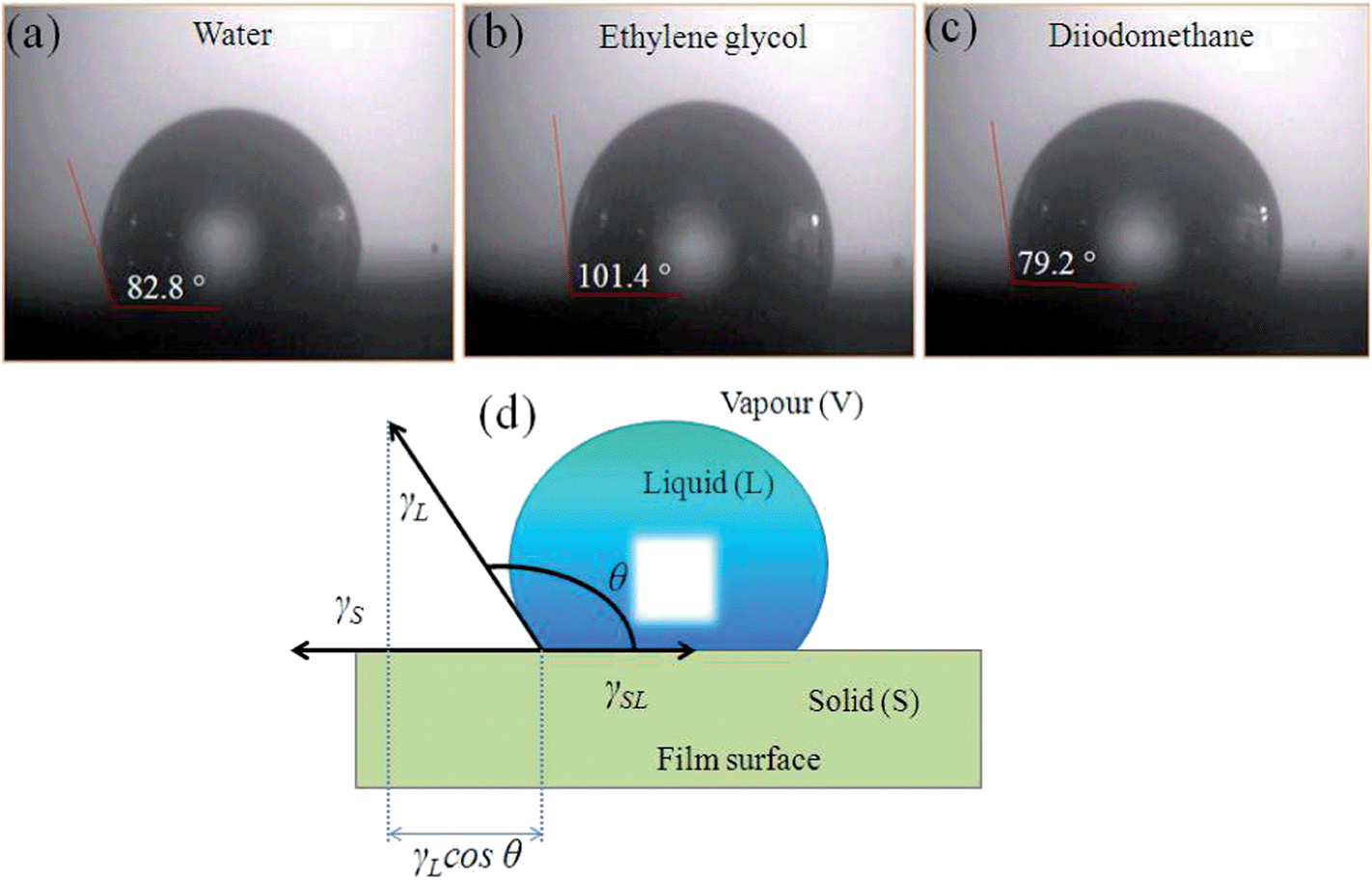
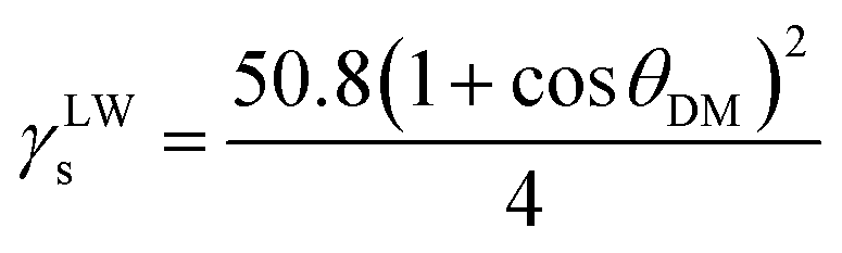
The total surface energy is another decisive scale parameter that affects the pattern formation of polymeric film on a plastic substrate. Surface free energy of the PS-b-PMMA film surface was calculated using the contact angles for three test liquids e.g. distilled water, ethylene glycol and diiodomethane. Since distilled water (DW), ethylene glycol (EG), and diiodomethane (DM) have different level of polarity. The contact angles of these liquids on the PS-b-PMMA layer were directly measured with the drop profile at the point of contact with the surface to estimate the surface free energy variation of these three different polar level liquids to the film. Fig. 2(a–c) shows the contact angles for DW, EG and DM measured on PS-b-PMMA surface on flexible PI substrate were 82.8°, 101.4°, and 79.2° respectively. This measurement technique is based on the Young–Dupre equation, as formulated by van Oss et al.15 which expresses the condition for equilibrium at a solid–liquid interface. To calculate the surface energy we design a simplified model as shown in Fig. 2(d) to describe the interfacial tension between the liquid (L) and the polymeric film surface (S).
 |
| | Fig. 2 (a–c) The contact angles for water, ethylene glycol, and diiodomethane measured on PS-b-PMMA surface on flexible PI substrate, and (d) a schematic representation of geometric parameters for determining interfacial energy and the contact angle of a liquid droplet wetted to a solid film surface. | |
The surface free energy was evaluated using van Oss and Good's three-liquid test method in together with the Lifshitz–van der Waals (LW) and Lewis acid-base (AB) theories,16 and the detailed energy contributions from the polymeric apolar and polar terms can be extracted individually. The total surface energy γs can be calculated from the combination of these three factors by using equation
| | |
γs = γLWs + γABs = γLWs + 2(γ+s)1/2(γ−s)1/2
| (1) |
where
γLWs is the Lifshitz–van der Waals component (apolar),
γABs is the Lewis acid-base component (polar),
γ+s is the Lewis acid and
γ−s is the Lewis base component. Further, the values of
γLWs,
γ+s and
γ−s were calculated from
eqn (2)–(4) after measuring the liquid–solid contact angle (
θ) for these three characterizing liquids
| |
 | (2) |
| |
 | (3) |
| |
 | (4) |
where
M and
N are defined as
19.76 + 36.4![[thin space (1/6-em)]](https://www.rsc.org/images/entities/char_2009.gif) cosθDW − 16.64cosθDM = M cosθDW − 16.64cosθDM = M |
| 6.21 + 25.4cosθEG − 19.19cosθDM = N |
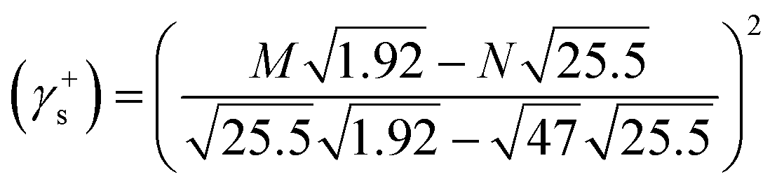
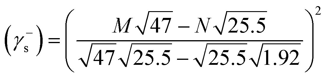
For the PS-b-PMMA composite film, the contact angles of DW, EG, and DM were 82.8°, 101.4°, and 79.2° respectively. Hence the calculated values of the surface energies γLWs, γ+s and γ−s by solving eqn (2)–(4) were 17.91 mJ m−2, 2.26 mJ m−2 and 32.51 mJ m−2, respectively. Thus, the total surface energy using eqn (1) for the PS-b-PMMA composite film was 35.05 mJ m−2. The results showed that the PS-b-PMMA composite film has low value for the Lifshitz–van der Waals (17.91 mJ m−2) and Lewis electron donor (32.51 mJ m−2). The surface free energy of the PS-b-PMMA film is composed of a high dispersive component and a low polar component. The composite film surface shows hydrophobic surface, but the P123 is a surfactant which contains a lot of –OH group and it is a hydrophilic material. As a result, removing the P123 causing the film has lower surface energy. In addition, in ZnO–TFT, the surface of the dielectric layer is important for effective performance because it allows for a conducting channel in the interface between the dielectric layer and the semiconductors.
2.3 Leakage current and capacitance tests of the PS-b-PMMA film into MIM capacitor device
Leakage current is a very important parameter to evaluate the dielectric behavior of the PS-b-PMMA film. For low-voltage operated electronic devices, leakage current should be low for improving switching speed of transistors and reduced the energy consumption. We measured leakage current by fabricate a MIM structured device by applying voltage to the PS-b-PMMA/Au/Cr contact to the bottom PI substrate and the Al top electrode (inset: Fig. 3(a)). As shown in Fig. 3(a), the leakage current density for the PS-b-PMMA was measured of 7.46 × 10⁻¹⁰ A cm−2. The result shows the dielectric performance of our sol–gel spin-coated polymeric PS-b-PMMA composite film is comparable to other various polymer as well as high-k dielectrics.17 This result is an average and based on the measurement of 20 devices on PI substrate for PS-b-PMMA gate dielectric.
 |
| | Fig. 3 (a) J–V plot (inset: MIM device configuration and a sample image), and (b) C–V plot for PS-b-PMMA film at frequency 100 kHz (inset: C–V plot for PS-b-PMMA film at frequency 1 kHz). | |
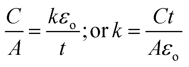
Further, we investigate the capacitance for our composite thin film to calculate the dielectric constant (k) value. Fig. 3(b) shows the capacitance–voltage (C–V) measurement of the PS-b-PMMA film in MIM capacitor device. The good capacitance (5.40 fF) was achieved at high frequency (100 kHz). We calculated the k-value of the PS-b-PMMA film using the following equation18
| |
 | (5) |
where
k is the dielectric constant of the dielectric layer,
εo ∼ 8.85 × 10
−12 F m
−1 and is the permittivity of vacuum,
A is the area of the capacitor (2.0 μm
2), and
t is the thickness of the PS-
b-PMMA film (14 nm). The calculated
k-value of the PS-
b-PMMA film was 4.2 at high frequency (100 kHz). We have pointed out from this result that the dielectric constant of PS-
b-PMAA at 100 kHz was high than its original
k-value between 2–2.7. We have then measured the capacitance (3.2 fF) at low frequency (1 kHz) as shown in inset of
Fig. 3(b), and the calculated dielectric constant is 2.5. This value is lies between its original dielectric constant. We have some discussion over this variation in dielectric constants. Since, the dielectric constant of any given material varies with temperature, and for polymers a rapid increase begins near their glass transition temperature. Dielectric constants also vary as a function of frequency, and this aspect will be important when we look at high frequency designs. Ideally, the dielectric constant should be constant with regard to frequency, temperature, voltage, and time. However, each polarization mechanism has a characteristic relaxation frequency. Therefore,
k values of most of the materials show a dependence on the frequency because slower mechanisms fail to respond and contribute to the dielectric storage when the frequency becomes large.
19 Moreover, polystyrene is non-polar and PMMA is polar, thus at high frequency due to polarization mechanism effect of PMMA work and this increase the dielectric constant of our film. It is also explained by D. Wei that the materials heterogeneity of a microphase-separated copolymer has an associated spatial variation in the dielectric constant.
20 We can drawn some conclusion here from these results that the leakage current density and the dielectric strength of the PS-
b-PMMA thin film are much better than those of the commonly used solution-processable polymer gate insulators. The obtained results indicate that the PS-
b-PMMA polymeric composite film as dielectric is a potential candidate to replace SiO
2 or other polymeric intermetal dielectric materials and that it could be an ideal alternative for flexible devices.
2.4 Reliability and air-stability test for the PS-b-PMMA composite dielectric film
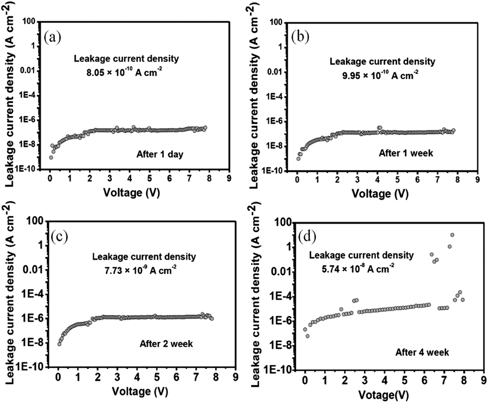
In order to realize the reliability and the stability of the PS-b-PMMA composite dielectric film, we measured electrical properties for the waiting period of time in air. The integrated MIM device on a PI cleaned Petridish at room temperature exposure to atmosphere and using four-point probe system, the leakage current densities were measured from day 1 to weeks 4 to check the device functionally working or damaged for this long duration of time. The results are shown in Fig. 4(a–d) for leakage current density measurements from day 1 to weeks 4 for the PS-b-PMMA film as gate dielectric layer. In the beginning of the stability test, the leakage current density of the newly made MIM capacitor was of 8.05 × 10⁻¹⁰ A cm−2. The leakage current density gradually increases to higher value after the waiting period for 1 week to 4 weeks. But after 2 weeks, the MIM capacitor device still shows a promising dielectric property, the leakage current density was about 7.73 × 10⁻⁹ A cm−2. Further, after 4 weeks or more the device properties go down to very high leakage current density i.e., 5.74 × 10⁻⁸ A cm−2. At this moment, the device properties hardly considered as an ideal device functioned well worth to be further use into transistor application. We conclude that the composite dielectric material deposit on a PI substrate showed good time stability. This result emphasized the importance of these tests in future to open up the way to further modification to be used for the long stability of time.
 |
| | Fig. 4 (a–d) Leakage current density measurements test for 1 day to 4 weeks for the PS-b-PMMA film as gate dielectric layer. | |
We have found the PS-b-PMMA composite film has high leakage current after 4 weeks. Because of the direct exposition of the device to air environment could be the cause of long-term stability of polymer based devices are affected by oxidative decomposition in air. In addition, the film at low thickness could suffers by deep-level defects due to long term explosion in air. If deep-level defects possibly touch each other and form a contact line but otherwise still can grow in all other directions, then the material of the contact line is drained. By this process two deep-level defects merge and form a single one and that is expected reason of high leakage current after 4 weeks. Although PS-b-PMMA is an organic composite materials film and oxidation in air might be expected, the device characteristics were essentially unchanged after 1 month; longer term stability has not been investigated. Further, we took double layer (thickness 28 nm) J–V measurement for PS-b-PMMA film and the device properties were found very stable and leakage current not even further changed while we put the sample in air-ambient condition for more than 1 month. The J–V results in air-ambient condition from day 1 to weeks 4 are shown in ESI Fig. S1.†
2.5 Performance of TFT with PS-b-PMMA as gate dielectric as ZnO as channel layer
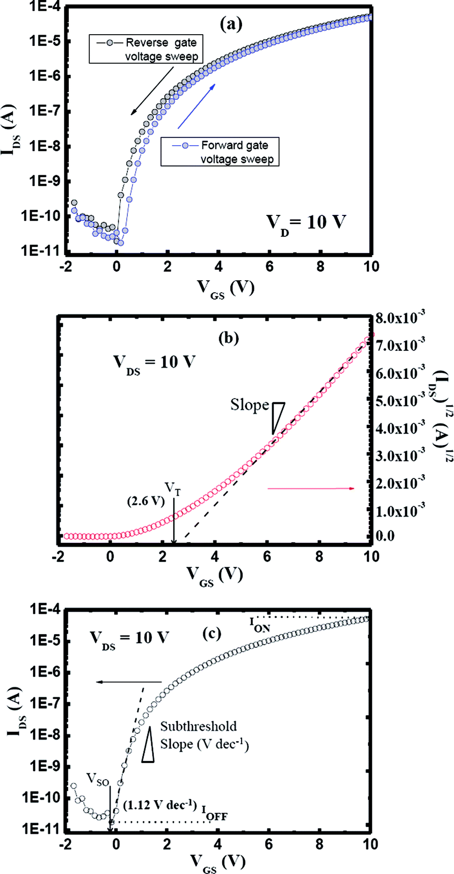
To investigate the potential of the PS-b-PMMA film as a gate dielectric and ZnO was used as a semiconductor channel layer for TFT on a plastic PI substrate with the sample photographic image is shown in Fig. 5(a) and the device geometry shown in Fig. 5(b). Fig. 1(c) show representative transfer characteristics (IDS–VGS), at VDS = 10 V, of our ZnO–TFT with the PS-b-PMMA film as a gate dielectric, respectively. As gate voltage increased, the increased drain current showed a good fit to the square relation in the saturation drain current equation;21| |
 | (6) |
where ID,sat is drain current in the saturation regime; W/L is the width to length ratio; μsat is mobility in the saturation regime; Ci is dielectric capacitance per unit area, VGS is gate voltage; and Vth is threshold voltage, which is estimated of 2.6 V. The highest saturation-region field-effect mobility obtained was about 2.48 cm2 V−1 s−1, which compared to maximum mobilities of 1 cm2 V−1 s−1 for a-Si:H TFTs as well more or less with the saturation-region field-effect mobility of TFTs reported by other groups.22 The Output characteristics of PS-b-PMMA as gate dielectric with ZnO as semiconductor were measured at 0–10 V with step of 2 V as shown in Fig. 5(d). Which showed the drain current saturated at a very low voltage, showing effective pinch off behavior. Our results suggest that deposition of the composite ternary system interlayer could be a simple and efficient surface-treatment of polymeric gate insulators for high-performance ZnO–TFTs.
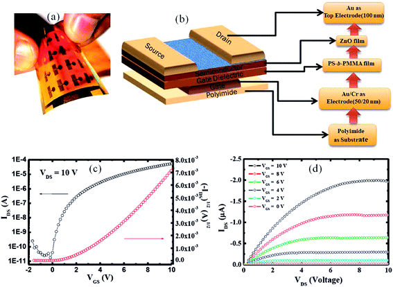 |
| | Fig. 5 (a) Photograph of the ZnO–TFT devices on a 5 cm × 5 cm area on flexible PI substrate, (b) schematic representation of the ZnO–TFT device that features PS-b-PMMA as a gate dielectric and ZnO as a semiconductor layer, (c) transfer characteristic (IDS–VGS), when VDS = 10 V, (d) output characteristic (IDS–VDS), where VGS ranges from 0 to 10.0 at 2 V step. | |
We have also characterized the hysteresis, threshold voltage (Vth), on/off current ratio (Ion/Ioff) and subthreshold slope (SS) for our PS-b-PMMA dielectric based ZnO–TFT. Fig. 6(a) shows the hysteresis in the transfer characteristics. The hysteresis (e.g., voltage shift (ΔV) between forward and reverse sweep) is related to charge (electron) trapping within the dielectric layer. The data showed almost negligible hysteresis (ΔV ∼ 0.12 V) for PS-b-PMMA film, suggesting a decrease in charge trapping for PS-b-PMMA–ZnO interface. The negligible hysteresis could be due to low thickness of PS-b-PMMA gate dielectric film. But there is an obvious trend of hysteresis as a function of the gate dielectric is observed. It can be attributed to the PS-b-PMMA layer, which fails to attain the charge injection from the gate electrode to the dielectric-semiconductor interface. When a negative sweep is applied to the gate electrode, then electrons are easily injected into the gate dielectric. Occurring at the same time, holes in the semiconductor layer are easily retained in the hole-traps. This verifies the hysteresis reduction effect of the composite (or hybrid) gate dielectric for wide range of channel lengths. Further, we have deducted Vth, and SS by using Fig. 6(b and c) respectively.
 |
| | Fig. 6 Extraction of the PS-b-PMMA gate dielectric ZnO–TFT from transfer characteristics (a) plot for hysteresis, (b) plot for deducing VT, and (c) plot for deducing subthreshold slope. | |
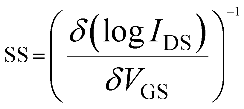
The threshold voltage (Vth) is estimated by the extrapolation of the linear portion of the transfer characteristic graph to the VGS axis as shown in Fig. 6(b). The estimated value of Vth from this graph is 2.6 V. Further, to analyze the subthreshold behavior of the device, the switch-on voltage (Vso) and inverse subthreshold slope (SS, V dec−1) are studied. The Vso is defined as the gate voltage where the current starts to increase in the semi-logarithmic IDS–VGS plot. The SS-value is calculated about 1.12 V dec−1 from the graph shown in Fig. 6(c) using the relation;23
| |
 | (7) |
The result obtained here, 1.12 V per decade, is larger than that typically observed for a-Si:H devices, but it is considerable enough to allow plastic ZnO–TFT use in many applications. In addition, we have also estimated the Ion/Ioff current ratio for ZnO–TFT device by using Fig. 6(c). The estimated Ion/Ioff current ratio is 3.12 × 10⁶ at VDS = 10 V. These device parameters for our organic composite dielectric and ZnO semiconductor based TFT device are comparable to results typically obtained for a-Si:H based TFT devices.
2.6 Environment-stability and bendability test for ZnO–TFT
For practical applications, bending test in tensile as well compressive mode and environment-stability test of our flexible TFT is a matter of concern due to oxygen and moisture trapping charge in degradation of the device properties. The environment-stability test of the ZnO based TFT on PS-b-PMMA dielectric, was monitored by measuring their mobility, and on/off current ratio as a function of time from day 1 to week 4 as shown in Fig. 7. The ZnO–TFT performance on PS-b-PMMA dielectric exhibited good ambient stability on a flexible PI substrate. However, after exposure in the air for more than 4 week, the ZnO–TFT on the PS-b-PMMA dielectric exhibited slight changes in mobility from 2.48 cm2 V−1 s−1 to 1.76 cm2 V−1 s−1, and on-off current ratio from 3.12 × 10⁶ to 8.40 × 10⁴. This change could be considered due to the changes in relative humidity for organic dielectric materials in the ambient condition, which has also been reported for other organic dielectric materials.24 All measurements reported here were made in room air with no precautions taken to prevent degradation of the TFT device. Although our organic composite materials film is a fairly sensitive material and oxidation in air might be expected, the device characteristics were essentially changed for low thickness of PS-b-PMAA after 1 month and no longer has term stability been investigated. Since, ambient air stability is very important for current organic materials based electronic devices, thus we tried passivation layer (double layer of PS-b-PMMA with thickness about 28 nm) to get long term stability in TFT device characteristics. Then, no appreciable changes in the transfer characteristics were observed for ZnO–TFT measured in air and stored under ambient conditions for one month (ESI, Fig. S2†). We have added these double layers PS-b-PMMA based ZnO–TFT results of mobility and on/off current ratio changes shown in inset of Fig. 7 to compare with single layer PS-b-PMMA based ZnO–TFT performance for day 1 to 4 weeks. Finally, it can be concluded from these results that the interface between polymer composite materials film as a gate dielectric layer and inorganic materials film as semiconductor layer is good and stable combination for future cheap plastic electronics.
 |
| | Fig. 7 The performance changes in terms of mobility and on/off current ratio of PS-b-PMMA film as gate dielectric and ZnO as semiconductor and while the ZnO–TFT device was bended in tensile and compressive mode (inset: bended graphic sample images) exposed in the ambient condition for day 1 to week 4 under bending test. (Insets: their corresponding characteristics for double layer PS-b-PMMA film under similar bending mode and exposed in the ambient condition up to 4 weeks.) | |
3. Conclusion
We have demonstrated here the composition of appropriate commercially available polymers and surfactant cross-linking agents affords robust, smooth, adherent, high surface energy, pinhole free, ultrathin (e.g., 14 nm) film showed low leakage current and good capacitance as a composite dielectric materials. The PS-b-PMMA film was readily deposited from sol–gel solution, which adheres strongly on a flexible PI substrate and compatible with ZnO semiconductor to be used into TFT application. The resulting ZnO–TFT and complementary MIM capacitor devices function at unprecedentedly low operating voltages for a polymer-based gate dielectric for single layer (14 nm thick) showed short term stability and for double layer (28 nm thick) showed good and long term stability. In this condition device performed functionally well even after waiting period of more than a month in air-ambient condition in together bending the sample in compressive and tensile mode. These results clearly shows that implementing the polymer ternary dielectric system using solution-processing methodologies offers low voltage, low power operation to be used into electronic applications.
4. Experimental section
4.1 Reagents and materials
Polyimide: DuPont™ Kapton® polyimide tape (abbreviated as PI) 38 μm in thickness a polymer of imide monomers was used a flexible substrate to characterize the surface and electrical properties of the PS-b-PMMA composite thin-film. The thermal stability of Kapton PI tape is excellent and allows processing temperature in excess of nearly 400 °C. Ethanol (C2H5OH), 95% solution purchase from Sigma Aldrich and used as solvent and cleanser. Deionized (DI) and distilled water: the water used was purified with filters, reverse osmosis, and de ionized system until the resistance was more than 18 MΩ cm−1. DI water was used to clean, wash, and be a solvent. Pluronic® P123 Block Copolymer Surfactant: Pluronic P123 triblock copolymer, HO(CH2CH2O)20(CH2CH(CH3)O)70(CH2CH2O)20H, (abbreviated as P123 or EO20PO70EO20, MW = 5800, BASF Corporation). In general, water-soluble triblock copolymers of poly(ethylene oxide) (PEO) and poly(propylene oxide) (PPO), as often denoted PEO–PPO–PEO, are commercially available nonionic macromolecular surface active agents. Primary hydroxyl groups a nonionic surfactant that is 100% active and relatively nontoxic. Polystyrene (PS): ((C8H8)n, Mw = 54000, Aldrich), poly(methyl methacrylate) (PMMA): ((C5O2H8)n, Mw = 54000, Aldrich) is a strong and lightweight material. PMMA ignites at 460 °C (860 °F) and burns, forming carbon dioxide, water, carbon monoxide and low-molecular-weight compounds, including formaldehyde. Toluene (C6H5CH3, Tedia Co. Inc.) was used as a solvent. The 50 nm thick ZnO layers were deposited at room temperature by radio-frequency (RF) magnetron sputtering with different Ar and O2 mixed gas ratios (pure Ar flow, Ar:O2 = 3:1, and 2:1). Chromium (Cr) shots, 99.999%, ADMAT Inc., size: 3–5 mm, aluminum (Al) shots, 99.999%, ADMAT Inc., size: 3–5 mm, gold (Au) shots, 98.999%, ADMAT Inc., size: 1–2 mm. The Cr, Al and Au films to be used as an electrode were deposited over PI substrate by a thermal coater evaporation system which Cr, Al and Au shots and tungsten boat were used during deposition process. All of the reagents and precursors were used without the further purification. Note that all of the experiments were performed in air or in a standard fume hood.
4.2 Precursor preparation of the PS-b-PMMA layer solution
In a typical synthesis experiment, PMMA (0.15 g) and PS (0.05 g) was added to a mixture of P123 (1.0 g) into toluene (15 mL) under static conditions. The reaction mixture is then stirred for 12 h using a magnetic stirrer at room temperature. After PMMA and PS were completely dissolved into toluene, the solution was used to prepare the PS-b-PMMA composite thin film. The mixed solution was then applied by spin-coating onto a flexible PI substrate in two steps (2000 rpm 20 s and 3000 rpm 30 s). Before thin film deposition, the PI tape was pasted onto glass substrate then dipped into alcohol and later into DI water for 5–10 s and then withdrawn for cleaning. Second, the substrate was cured in a vacuum oven at 100 °C for 10 min. Then, further surface characterizations and applications in electronic devices (MIM and TFT) were investigated.
4.3 Fabrication of the MIM and ZnO–TFT devices
DuPont Kapton plastic PI substrate with a thickness of 38 μm was used as the flexible substrate for fabricating the MIM and ZnO–TFT devices. The PI substrate was ultrasonically cleaned using ethanol (Fluka; water content: <0.1%) for 30 min and then rinsed with DI water. A high-pressure stream of N2 gas was then used to remove the water and any remaining particles from the PI surface. After being cleaned, the PI substrate was annealed at 200 °C for 1 h under vacuum to achieve relative thermal stability and to enhance the adhesion strength. Next, Cr (20 nm thick) and Au (80 nm thick) were sequentially deposited onto the PI substrate using a thermal coater. Au was deposited as a gate electrode over the Cr layer on the PI substrate. The PS-b-PMMA film, which functioned as the dielectric layer, was deposited using spin-coating and then cured it in a vacuum oven at 100 °C for 5 min. At the end of the experiments, Al films with a thickness of 300 nm were pattered as the top electrode using a shadow mask and a thermal coater. The electrical insulating properties of the PS-b-PMMA composite film have been optimized for MIM device on the PI substrate, which makes them suitable candidates for use as a stable intermetal dielectric in advanced flexible electronic devices. Further for ZnO–TFT device fabrication, Cr and Au, which had thickness of 20 nm and 80 nm, respectively, were sequentially deposited through a shadow mask using a thermal coater to function as gate electrodes. Then, PS-b-PMMA film was deposited using the solution spin-coating process as described in the previous section to function as an insulator layer. ZnO film was then deposited on the PS-b-PMMA/Au/Cr/PI substrate by RF magnetron sputtering as a channel layer with the substrate temperature maintained at room temperature. Finally, source (S) and drain (D) Au electrodes with a thickness of 100 nm were deposited which yielded the top-contact electrode ZnO–TFT. The channel length (L) and width (W) were 70 and 1500 μm, respectively.
4.4 The PS-b-PMMA thin-film characterizations and device performance analysis
The surface morphology of the PS-b-PMMA film that coated on a PI substrate was evaluated using atomic force microscopy (AFM, Digital Instruments Nanoscope, D-5000) with a scan size of 2 μm × 2 μm and a scan rate of 1 Hz. Two methods were used to determine the film thickness. We used ellipsometry techniques and 2-D AFM image cross section line analyses to measure the thickness of the thin film. The FT-IR spectrum was recorded with the samples in KBr pellets (2 mg per 300 mg KBr) on an FT-IR spectrometer (model 580, Perkin-Elmer) with a resolution of 4.00 cm−1. An infrared spectrum was recorded in the range of 500–4000 cm−1 to determine the functional groups in the molecular structure. The FT-IR measurement was performed at room temperature. The water contact angle on the film surface was measured using a commercial contact angle meter. Distilled water, ethylene glycol and diiodomethane were used as the test liquids during the contact angle experiment to calculate the surface energy. The contact angles were measured using a FTA program after the drop made contact with the film surface during testing of the flexible PI substrate. The leakage currents and capacitances in the MIM structured device with the composite film were measured using an Agilent-4156 probe station and an HP-4284A capacitance–voltage analyzer, respectively. The output and transfer characteristics of the OTFT were measured using an Agilent-4156 probe station under ambient conditions.
Acknowledgements
We gratefully acknowledge the National Nano Device Laboratories (NDL) and the National Science Council (NSC) of Taiwan for financial support this research under the contract NSC 101-2113-M-009-007-MY3.
Notes and references
- K. Nomura, H. Ohta, A. Takagi, T. Kamiya, M. Hirano and H. Hosono, Nature, 2004, 432, 488 CrossRef CAS PubMed.
- L. Wang, M.-H. Yoon, G. Lu, Y. Yang, A. Facchetti and T. J. Marks, Nat. Mater., 2006, 5, 893 CrossRef CAS PubMed.
- M. Roschke and F. Schwierz, IEEE Trans. Electron Devices, 2001, 48(7), 1442 CrossRef CAS.
-
(a) S.-H. Lee, W.-S. Hong, J.-M. Kim, H. Lim, K.-B. Park, C.-L. Cho, K.-E. Lee, D.-Y. Kim, J.-S. Jung, J.-Y. Kwon and T. Noguchi, Jpn. J. Appl. Phys., 2006, 2(45), L227 CrossRef;
(b) A. Sazonov, M. Meitine, D. Stryakhilev and A. Nathan, Semiconductors, 2006, 40, 959 CrossRef CAS.
- E. M. Vogel, K. Z. Ahmed, B. Hornung, W. K. Henson, P. K. McLarty, G. Lucovsky, J. R. Hauser and J. Wortman, IEEE Trans. Electron Devices, 1998, 45, 1350 CrossRef CAS.
- C.-H. Ting and T. E. Seidel, Method and Needs for Low k Materials Research, Low Dielectric Constant Materials-Synthesis and Applications in Microelectronics, PA Materials Research Soc., Pittsburgh, 1995, vol. 381, p. 3 Search PubMed.
- J. N. Tiwari, J. S. Meena, C.-S. Wu, R. N. Tiwari, M.-C. Chu, F.-C. Chang and F.-H. Ko, ChemSusChem, 2010, 3, 1051 CrossRef CAS PubMed.
-
(a) C. Kim, A. Facchetti and T. J. Marks, Science, 2007, 318, 76 CrossRef CAS PubMed;
(b) Z. Ahmad, Polymeric Dielectric Materials, licensee InTech, 2012 Search PubMed;
(c) T.-S. Huang, Y.-K. Su and P.-C. Wang, Appl. Phys. Lett., 2007, 91, 092116 CrossRef;
(d) M.-H. Yoon, H. Yan, A. Facchetti and T. J. J. Marks, J. Am. Chem. Soc., 2005, 127, 10388 CrossRef CAS PubMed.
-
(a) Y.-Y. Noh and H. Sirringhaus, Org. Electron., 2009, 10, 174 CrossRef CAS;
(b) J. S. Meena, M.-C. Chu, Y.-C. Chang, C.-S. Wu, C.-C. Cheng, F.-C. Chang and F.-H. Ko, ACS Appl. Mater. Interfaces, 2012, 4, 3261 CrossRef CAS PubMed.
- P. Barber, S. Balasubramanian, Y. Anguchamy, S. Gong, A. Wibowo, H. Gao, H. J. Ploehn and H.-C. Z. Loye, Materials, 2009, 2, 1697 CrossRef CAS.
- K.-S. Jang, D. Wee, Y. H. Kim, J. Kim, T. Ahn, J.-W. Ka and M. H. Yi, Langmuir, 2013, 29, 7143 CrossRef CAS PubMed.
-
(a) M.-C. Chu, J. S. Meena, P.-T. Liu, H.-P. D. Shieh, H.-C. You, Y.-W. Tu, F.-C. Chang and F.-H. Ko, Appl. Phys. Express, 2013, 6, 076501 CrossRef;
(b) J. S. Meena, M.-C. Chu, Y.-C. Chang, H.-C. You, R. Singh, P.-T. Liu, H.-P. D. Shieh, F.-C. Chang and F.-H. Ko, J. Mater. Chem. C, 2013, 1, 6613 RSC.
- C. Üzüm, J. Hellwig, N. Madaboosi, D. Volodkin and R. von Klitzing, Beilstein J. Nanotechnol., 2012, 3, 778 CrossRef PubMed.
- K. Kaniappan and S. Latha, Int. J. ChemTech Res., 2011, 3(2), 708 CAS.
- C. J. van Oss, M. K. Chaudhary and R. J. Good, Chem. Rev., 1988, 88, 927 CrossRef CAS.
-
(a) H. Chen, L. Li, P. M. Jones, Y.-T. Hsia and M. S. Jhon, IEEE Trans. Magn., 2007, 43(6), 2226 CrossRef CAS;
(b) F.-H. Ko, C.-T. Wu and T.-C. Chu, Appl. Phys. Lett., 2007, 90, 191901 CrossRef PubMed.
-
(a) J. Rudd, Physical Constants of Poly(styrene), in Polymer Handbook, ed. J. Brandrup and E. Immergut, John Wiley & Sons, New York, 3rd edn, 1989 Search PubMed;
(b) W. Wunderlich, Physical Constants of Poly(methyl methacrylate), in Polymer Handbook, ed. J. Brandrup and E. Immergut, John Wiley & Sons, New York, 3rd edn, 1989 Search PubMed;
(c) N. Kameda, T. Nishiguchi, Y. Morikawa, M. Kekura, H. Nonaka and S. Ichimura, J. Electrochem. Soc., 2007, 154, H769 CrossRef CAS PubMed;
(d) M.-H. Yoon, H. Yan, A. Facchetti and T. J. Marks, J. Am. Chem. Soc., 2005, 127, 10388 CrossRef CAS PubMed;
(e) Y. Q. Wu, H. C. Lin, P. D. Ye and G. D. Wilk, Appl. Phys. Lett., 2007, 90, 072105 CrossRef PubMed;
(f) J. S. Meena, M.-C. Chu, C.-S. Wu, S. Ravipati and F.-H. Ko, J. Nanosci. Nanotechnol., 2011, 11, 6858 CrossRef CAS PubMed;
(g) J. S. Meena, M.-C. Chu, S.-W. Kuo, F.-C. Chang and F.-H. Ko, Phys. Chem. Chem. Phys., 2010, 12, 2582 RSC.
-
(a) A. Facchetti, M.-H. Yoon and T. J. Marks, Adv. Mater., 2005, 17, 1705 CrossRef CAS;
(b) C. Wang, W.-Y. Lee, R. Nakajima, J. Mei, D. H. Kim and Z. Bao, Chem. Mater., 2013, 25, 4806 CrossRef CAS.
- A. R. Blythe, Electrical Properties of Polymers, Cambridge University Press, Cambridge, 1979 Search PubMed.
- D. Wei, Electrochemical Nanofabrication: Principles and Applications, Pan Stanford Publishing Pte. Ltd, 2012 Search PubMed.
- R. Hofmockel, U. Zschieschang, U. Kraft, R. Rödel, N. H. Hansen, M. Stolte, F. Würthner, K. Takimiya, K. Kern, J. Pflaum and H. Klauk, Org. Electron., 2013, 14, 3213 CrossRef CAS PubMed.
-
(a) R. A. Street, Technology and Applications of Amorphous Silicon, Springer-Verlag, Berlin Heildlberg, Germany, 2000 Search PubMed;
(b) J.-S. Seo, J.-H. Jeon, Y. H. Hwang, H. Park, M. Ryu, S.-H. K. Park and B.-S. Bae, Sci. Rep., 2013, 3, 2085 CrossRef PubMed.
- J. H. Seo, J.-H. Kwon, S.-I. Shin, K.-S. Suh and B.-K. Ju, Semicond. Sci. Technol., 2007, 22, 1039 CrossRef CAS.
- D. Li, E.-J. Borkent, R. Nortrup, H. Moon, H. Katz and Z. Bao, Appl. Phys. Lett., 2005, 86(4), 042105 CrossRef PubMed.
Footnote |
| † Electronic supplementary information (ESI) available. See DOI: 10.1039/c4ra01517g |
|
| This journal is © The Royal Society of Chemistry 2014 |
Click here to see how this site uses Cookies. View our privacy policy here.