High-efficiency CdTe thin-film solar cell with a mono-grained CdS window layer
Ruilong
Yang
a,
Dezhao
Wang
a,
Lei
Wan
b and
Deliang
Wang
*a
aHefei National Laboratory for Physical Sciences at the Microscale, University of Science and Technology of China, Hefei, Anhui 230026, People's Republic of China. E-mail: eedewang@ustc.edu.cn; Fax: +86 55163606266; Tel: +86 55163600450
bSchool of Electrical Engineering and Automation, Hefei University of Technology (HFUT), Hefei, Anhui 230009, People's Republic of China
First published on 23rd April 2014
Abstract
High-crystalline-quality CdS thin films with a mono-grained layer of submicron grain size were successfully fabricated. CdS thin films prepared by chemical bath deposition were re-crystallized under different chemical atmospheres. The microstructure of the CdS films, the hetero-junction interface CdS/CdTe, and therefore the solar cell performance were critically dependent on the film process history of the window CdS layers. Heat treatment of a CdS precursor film coated with a CdCl2 layer and under a high CdCl2 vapor pressure reduced over-oxidation at the grain surface and promoted in-plane grain coalescence along the CdS/FTO (F-doped SnO2) interface. A high-crystalline-quality, mono-grain CdS layer ensured homogenous intermixing of CdS and CdTe at the junction interface. A short-circuit current as high as 25.1 mA cm−2 was obtained for a mono-grain-CdS/CdTe solar cell. The corresponding solar cell efficiency is 14.6%.
1. Introduction
CdTe has proved itself to be a leading candidate for the development of cost-effective photovoltaic devices among second-generation solar cells. The most efficient hetero-junction partner for the absorber CdTe in a solar cell is CdS, which is usually referred to as the window layer.1 A typical CdTe thin film solar cell has the structure of glass/SnO2:F(FTO)/CdS/CdTe/metal back electrode.2,3 Sunlight photons transmit through an N-type CdS window layer and are efficiently absorbed in the absorber CdTe film. CdS has a band gap of 2.42 eV, corresponding to a photon absorption threshold with a light wavelength of ∼517 nm. In a CdS/CdTe heterostructural solar cell, the CdS layer thickness is usually about 150–300 nm.4 Photogenerated carriers in the CdS layer almost completely recombine within it and do not contribute to the photocurrent. The photocurrent loss due to light absorption in a thick CdS layer was estimated to be relatively high, ∼7 mA cm−2. Therefore, a thin CdS layer with a thickness less than 100 nm is desired for fabrication of high-efficiency CdTe solar cells. However, when the thickness of a CdS layer is decreased to several tens of nanometers, the so-called pinhole would be almost formed unavoidably.1,4 Also because of the reduced thickness, part of the CdS in the weak area could be easily consumed through reaction with CdTe during the subsequent deposition of the absorber layer and/or thermal activation process, leading to direct contact of CdTe with the front electrode (circuit shorting). These two unwanted macroscopic defects in a CdS/CdTe solar cell, which are often observed in the laboratory, are shown in Fig. 1. Shorting in a CdTe solar cell causes a sharp decline of both the open-circuit voltage and the fill factor. Post-deposition annealing in the presence of cadmium chloride (CdCl2) is an important device fabrication step to obtain a highly efficient CdTe solar cell. It is recognized that the CdCl2 treatment can increase the grain size of both CdS and CdTe, passivate the grain boundary and reduce lattice mismatch through the formation of CdSxTe1−x at the CdS/CdTe interface.5,6 Because of the small thickness of the CdS window layer, any change in the microstructure or the stoichiometry of CdS caused by thermal heat treatment and/or the activation process would have a strong effect on a CdTe solar cell, as can be seen in this study. At the interface of CdS/CdTe, considerable interdiffusion/reaction between CdS and CdTe has been reported both by us and other researchers.1,3 This is understandable considering that both CdS and CdTe compounds belong to the II–VI semiconductors and have similar chemical properties. Excessive consumption of CdS can lead to the shunting/shoring path, and thus limit device performance. During the vapor CdCl2 treatment, increased grain size due to promoted recrystallization may introduce stress at the TCO/CdS interface, leading to blistering or even to peeling of a CdS film.6 If the CdS layer is not treated before the CdTe deposition, excessive interdiffusion would occur at the CdS/CdTe interface during the process of CdCl2 treatment for CdTe, leading to low efficiency of a cell device.7 Theoretically, as an N-type window layer in a CdTe solar cell, CdS should be as thin as possible and at the same time chemically robust enough to avoid formation of pinholes and current-shunting paths. During the thermal treatment of both a CdS and a CdTe layer in CdCl2, oxygen is intentionally introduced into the annealing chamber. Also oxygen is introduced into the CdTe deposition chamber to control the CdTe nucleation on CdS/FTO/glass substrates during the initial CdTe growth. Oxygen plays an important role in CdCl2 heat treatment for CdS. The prominent effect is to restrict in-diffusion of Te and out-diffusion of S at the CdS/CdTe junction interface, and this can lead to minimized interdiffusion at the interface.8 The limited interdiffusion at the interface creates a CdTe cell that has a high response at short wavelengths near the CdTe absorption edge.9 Hence, thermal treatment of a CdS layer with the presence of Cl and O prior to CdTe deposition makes it possible to employ a thin CdS film as the window layer in a CdTe solar cell. In this study, experimental effort was focused on fabricating high-crystalline-quality CdS thin films through re-crystallization under different chemical annealing atmospheres. The aim of this study was to find a relatively simple and robust way to obtain a mono-grained CdS layer. A thin mono-grained CdS layer can reduce carrier scattering at grain boundaries, enhance light transmission, and therefore increase short-circuit current and cell efficiency. Systematic investigation of recrystallization of CdS precursor layers prepared by chemical bath deposition demonstrated that the kinds of point defects, the surface stoichiometry, and the recrystallization/coalescence of nano-sized grains of a precursor layer depended critically on the dynamic process, which was carried out in an annealing atmosphere with the presence of CdCl2 and oxygen. As shown in this study, a high-crystalline-quality mono-grained CdS layer makes formation of a very uniform CdS/CdTe junction possible, both geometrically and stoichiometrically. We found that the CdS/CdTe junction quality and cell performance depended critically on the experimental dynamic processes to anneal the CdS layers.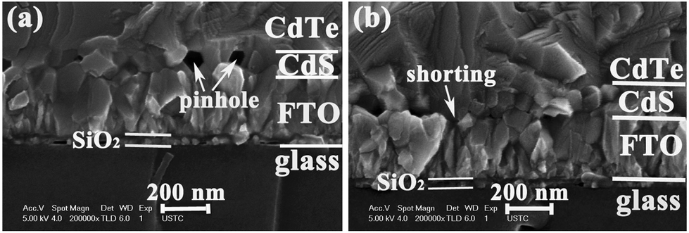 | ||
| Fig. 1 SEM cross-sectional microstructures of two CdTe solar cells showing unwanted macroscopic defects of (a) pinhole and (b) direct contacts (shorting) at the CdS/CdTe interfaces, respectively. | ||
2. Experimental section
In this study, the CdS precursor films were deposited on glass substrates coated with F-doped SnO2 (FTO) by the chemical bath deposition (CBD) technique. The aqueous solution was composed of deionized water, cadmium acetate, ammonium acetate, and thiourea. A certain amount of ammonia was added to modify the pH of the solution. During the CdS deposition, the glass cell was maintained at a temperature of 65 °C. P-type CdTe absorber layer was prepared in a homemade close-spaced sublimation apparatus on the glass/FTO/CdS templates. CdTe thin-film solar cells were prepared with a structure of glass/SnO2:F/CdS/CdTe/Cu:Au/Ag back electrode. The Cu/Au back contact was prepared by sequential thermal evaporation of Cu and Au in a vacuum chamber. The cell size was 5 × 5 mm2. Detailed film and cell fabrication procedures can be found in our previous work.3In this study, three kinds of heat treatment process for CdS recrystallization were carried out. A CdS precursor film prepared by CBD was first immersed into saturated CdCl2–methanol solution to dip-coat a thin CdCl2 layer and then heat treated in a furnace in air atmosphere at a temperature of 400 °C for 10 min. We call this sample the dip-coating CdS. This kind of heat treatment has been employed by certain researchers in the fabrication of CdTe solar cells. The second kind of heat treatment was carried out in a chamber filled with inert gas at a pressure of 0.7 atmosphere Ar. The aim of this process was to minimize the effect of oxygen and to enhance grain growth during CdS recrystallization. We call this sample the Ar-treated CdS. During the heat treatment, temperatures of the source and substrate were 390 °C and 400 °C, respectively. The purpose of the additional 10 °C for the substrate was to prevent CdCl2 deposition on the CdS films. The third kind of heat treatment was carried out as follows. A CdS precursor layer was first coated with a CdCl2 layer by dipping in the same saturated CdCl2–methanol solution as that used for the dip-coating sample and then heat treated in a chamber in the presence of CdCl2 vapor and air atmosphere. The heat treatment temperature and time duration were the same as that of the dip-coating CdS. We call this sample the coating-vapor CdS.
Morphological microstructures of films and cell junctions were characterized by using a field emission scanning electron microanalyser (SEM, Sirion 200). The crystalline structure of the films was studied by X-ray diffraction (XRD). The CdS film surface chemical states were analyzed by high-resolution, X-ray photoelectron spectroscopy (XPS). XPS measurements were performed on a Thermo VG Scientific ESCALAB 250 instrument. All XPS spectra were calibrated using the carbon C 1s peak (284.80 eV). Photoluminescence measurements of CdS films were carried out at room temperature with a FLUOROLOG-3-TAU spectrofluorometer. The wavelength of the exciting light was 458 nm. Device performances of CdTe solar cells were characterized by current density–voltage (J–V) curve and quantum efficiency measurements. The cell J–V curves were measured under standard AM1.5 (100 mW cm−2) illumination using a solar simulator (Oriel Sol 3A, USA), whose illumination intensity was calibrated by a monocrystalline silicon reference cell. The external quantum efficiencies (EQE) of the devices were measured from 300 to 1000 nm by using a hypermonolight system (Bunkoukeiki SM-250).
3. Results and discussions
Properties of the as-grown CdS films were characterized by various experimental methods. Fig. 2(a) shows the SEM cross-sectional morphology of a CBD as-grown CdS film. It consisted of nano-sized clusters, sized at ∼10 nm. Due to homogeneous CdS nucleation on the FTO, the CdS precursor film was uniform and smooth regarding film thickness and surface morphology. The tight attachment of CdS on the FTO/glass substrate is very important for obtaining high-quality CdS film after heat treatment. The relatively strong and sharp XRD diffraction peak at 26.7°, shown in Fig. 2(b), corresponds to the hexagonal phase H(002) and/or the cubic phase C(111).10 All other XRD peaks can be ascribed to the hexagonal phase, denoted as H in the figure. The crystalline structure of the CdS layer greatly affects the initial nucleation and growth of CdTe. Hexagonal CdS supports the formation of wurtzite CdTe, while cubic CdS favors the formation of sphalerite CdTe.8 We can see that the as-grown CdS precursor film had been already well crystallized to some extent. Fig. 2(c) shows the light transmittance of the film versus the photon wavelength, and Fig. 2(d) is a plot of (αhν)2versus photon energy, where α, h, and ν are the absorption coefficient, Planck constant and photon frequency, respectively. Light transmittance has a relatively large value of ∼75% above the absorption threshold of ∼510 nm (2.42 eV). In a CdTe solar cell, the light transmittance through CdS would be much larger than 75% due to both the crystalline recrystallization and the much reduced light reflection at the film/FTO/glass interface, as seen in this study. The band gap energy obtained from Fig. 2(d) is 2.47 eV, which is slightly larger than the generally recognized value of 2.42 eV. This is possibly due to the nano-sized CdS grains in the precursor layer. | ||
| Fig. 2 (a) SEM cross-sectional microstructure of an as-grown CdS film prepared by CBD; (b) X-ray diffraction spectrum of the as-grown CdS film; (c) transmittance spectrum of the as-grown CdS film; (d) (αhν)2versus photon energy (hν). | ||
Fig. 3 shows the SEM cross-sectional morphologies of dip-coating CdS films after heat treatment in air atmosphere for time periods of 15, 30 and 40 min. Compared to the as-grown CdS film, the films had recrystallized having a grain size of ∼40–50 nm. There were many small voids between the grains and they were not densely packed. This type of microstructure would induce formation of pinholes at the CdS/CdTe interface during the subsequent deposition of CdTe on CdS at a temperature of ∼550 °C, as seen in Fig. 4(a). As discussed above, considerable reaction between CdS and CdTe may occur and in some areas CdS might be totally consumed, leading to the formation of pinholes and shunting paths. We fabricated an inverted CdTe solar cell structure, namely, a 35 nm-thick CdS layer was deposited on the surface of a CdTe solar cell structure, to study the interdiffusion at the CdS/CdTe interface.3 Such a structure design allowed us to obtain strong scattering signals of Raman, X-ray diffraction, and XPS from the top CdS layer as well as from the CdS/CdTe interface. It was found that strong interdiffusion began to occur at a temperature of about 350 °C at the CdS/CdTe interface. Above a temperature of ∼400 °C, the CdS layer began to be quickly consumed through interdiffusion and reaction with CdTe. After heat treatment at a temperature of 550 °C, considerable interdiffusion of S and Te occurred to form S-rich and Te-rich CdSxTe1−x alloy with an x value of ∼10%. From Fig. 4(a) we can see that the density of the void and/or pinhole at the interface is relatively high when a CdTe solar cell employed a dip-coating CdS layer as the window layer. With longer heat treatment time, the CdS grain size was slightly increased and the density of voids between CdS grains was decreased, as can be seen in Fig. 3(c) and (d). The re-crystallization for the dip-coating CdS was not perfect enough for fabrication of highly efficient CdTe solar cells. The J–V curve of a CdTe solar cell with a dip-coating treated CdS window layer is shown in Fig. 4(b). The short-circuit current Jsc, the open-circuit voltage Voc, the fill factor FF, and the cell efficiency are 19.0 mA cm−2, 749 mV, 0.62, and 8.87%, respectively. The Voc and the FF are low due to the presence of shunting paths and the pinholes at the interface. After CdCl2 heat treatment, the dip-coating CdS film showed a weak peak at 48.1°, which corresponds to the H(103). A peak at 32.8° corresponding to the (103) atomic plane of CdO was observed. Its intensity was rather strong, indicating that relatively severe oxidation occurred in the dip-coating CdS film. The over-oxidation was responsible for the formation of voids and led to the not well-recrystallized CdS film. This was also confirmed by XPS measurements to be discussed in subsequent details.
 | ||
| Fig. 3 SEM cross-sectional morphologies of the dip-coating CdS films after annealed in the air atmosphere for different time period: (a) 15 min, (b) 30 min, and (c) 40 min, respectively; (d) X-ray diffraction spectrum of the CdS film treated for 15 min. | ||
 | ||
| Fig. 4 (a) SEM cross-sectional microstructure of a CdTe/CdS junction prepared with a dip-coating CdS window layer; (b) light current–voltage curve of the CdTe solar cell measured at AM 1.5 condition. | ||
In order to avoid over-oxidation and to enhance coalescence of nano-sized CdS grains, we heat treated CdS films in a chamber filled with Ar gas with a pressure of 0.7 atmospheres. The source of CdCl2, with a temperature of 390 °C, was closely placed near the CdS film surface to ensure a high CdCl2 vapor pressure. The spacing between the CdCl2 source and CdS film was 2–3 mm. Fig. 5 shows the SEM cross-sectional morphologies of CdS films after heat treatment in an Ar atmosphere for time periods of 5, 10 and 30 min. After the 30 min treatment, a mono-grained CdS film was obtained, namely, the CdS film was composed of only one layer of grains with a size of 100–400 nm. We found that after only 5 min, a mono-grained CdS layer had already been formed with well-defined crystalline facets (see Fig. 5(b)). The CdS grains were densely packed on the FTO surface. The 30 min-treated film had a relatively large grain-size distribution, with some too-large and too-small CdS grain sizes. Such film microstructure is not good for solar cell fabrication.
 | ||
| Fig. 5 (a, c and e) SEM surface morphologies, and (b, d and f) SEM cross-sectional morphologies of the CdS films after heat treatment in Ar atmosphere for different time period of 5, 10, and 30 min, respectively. | ||
Fig. 6(a) shows the XRD spectra of the as-grown film and the films after 5- and 10 min heat treatments. After the 10 min heat treatment, the H(002) peak showed much enhanced intensity and decreased peak width, indicating that the crystalline quality was relatively good. The H(002) peak also moved to a smaller 2Θ value with increased heat treatment time, indicating that the lattice parameter became smaller compared to the as-grown precursor layer. The energy band gaps of the 5 and 10 min heat-treated films, which were obtained using light transmittance spectra, are 2.41 and 2.43 eV (see Fig. 6(b)), respectively. These values are almost the same as that of bulk CdS. Above the absorption threshold the two curves in Fig. 6(b) increased sharply.
 | ||
| Fig. 6 (a) X-ray diffraction spectra and (b) (αhν)2versus photon energy of the CdS films before and after heat treatment in Ar atmosphere. | ||
All this information indicates that the CdS films had been well recrystallized after heat treatment in an Ar atmosphere in the presence of high-pressure CdCl2. However, CdTe solar cells fabricated with the Ar-treated CdS window layers demonstrated much worse device performance compared to other solar cells presented in this study. Fig. 7(a) shows the SEM cross-sectional microstructure of a CdTe solar cell with an Ar-treated CdS window layer heat treated for 5 min. We can see that at the interface the two materials of CdTe and CdS were totally mixed together. The interface between CdTe and CdS is not easily identified, indicating that the extent of interdiffusion and/or reaction was much larger than the cell with a dip-coating CdS film shown in Fig. 4(a). This result is consistent with the study by Albin et al.8 They reported that when low-oxygen-containing CdS films were used as window layers, sulfur diffusion was substantial, leading to significant consumption of the CdS layers. In Fig. 7(a) we can see that the CdTe absorber layer had a very good crystalline structure due to the well-relieved lattice mismatch between CdS and CdTe through formation of the alloy CdSxTe1−x. However, the cell efficiency is very low, only 1.91%. The short-circuit current Jsc, the open-circuit voltage Voc, and the fill factor FF are only 6.25 mA cm−2, 680 mV and 0.45, respectively. The external quantum efficiency (EQE) measurement is shown in Fig. 7(c). The cell shows a rather low EQE with a value of only ∼20–30% in the wavelength range of ∼500–800 nm. In addition, cell EQE, which had 14.6% efficiency (to be discussed in the following), with a coating-vapor CdS as window layer, is included in the figure for comparison. We can see that the EQE curve of the cell with the Ar-treated CdS as the window layer can be divided into three parts according to EQE versus wavelength, namely, wavelength ranges of ∼300–510 nm, 510–800 nm, and 800–860 nm. The vertical lines in the figure at 510 and 860 nm correspond to the optical absorption threshold of the CdS and the CdTe, respectively. The shape of the EQE curve at the 300–800 nm wavelength is quantitatively similar to the theoretical calculation of Albin et al.8 The n-type alloy layer CdSxTe1−x simply attenuated the beam without contributing to the photocurrent. The much reduced EQE suggested that the alloy layer CdSxTe1−x was relatively thick, that is, much thicker than 100 nm.8 The diffusion of Te from CdTe into the CdS considerably enhanced the light absorption in CdS, leading to much reduced EQE at the range of 300–510 nm compared with the cell with a vapor-coating CdS window layer. Te diffusion into the CdS layer produced the CdS1−xTex ternary compound, which has a lower band gap than that of the CdS, and light absorption was increased in the window layer. Considering that CdTe is a direct band gap semiconductor and it has a high absorption coefficient, photons with short wavelength of 500–800 nm are mostly absorbed in CdTe near the light-incident front CdS/CdTe interface. In the ideal case, the density of the photon-generated carrier is decreased exponentially away from the interface. The much reduced EQE spectrum at 510–800 nm implies that an almost “dead” layer was formed through too much interdiffusion/reaction at the interface. The majority of the photo-generated carriers were recombined before they could be efficiently separated by the built-in electric field, if it existed, at the heterojunction. Photons with longer wavelengths of ∼800–860 nm could travel deeper into the CdTe away from the interface and were then efficiently absorbed and separated, leading to higher EQE than that of the photons with wavelengths of ∼500–800 nm.
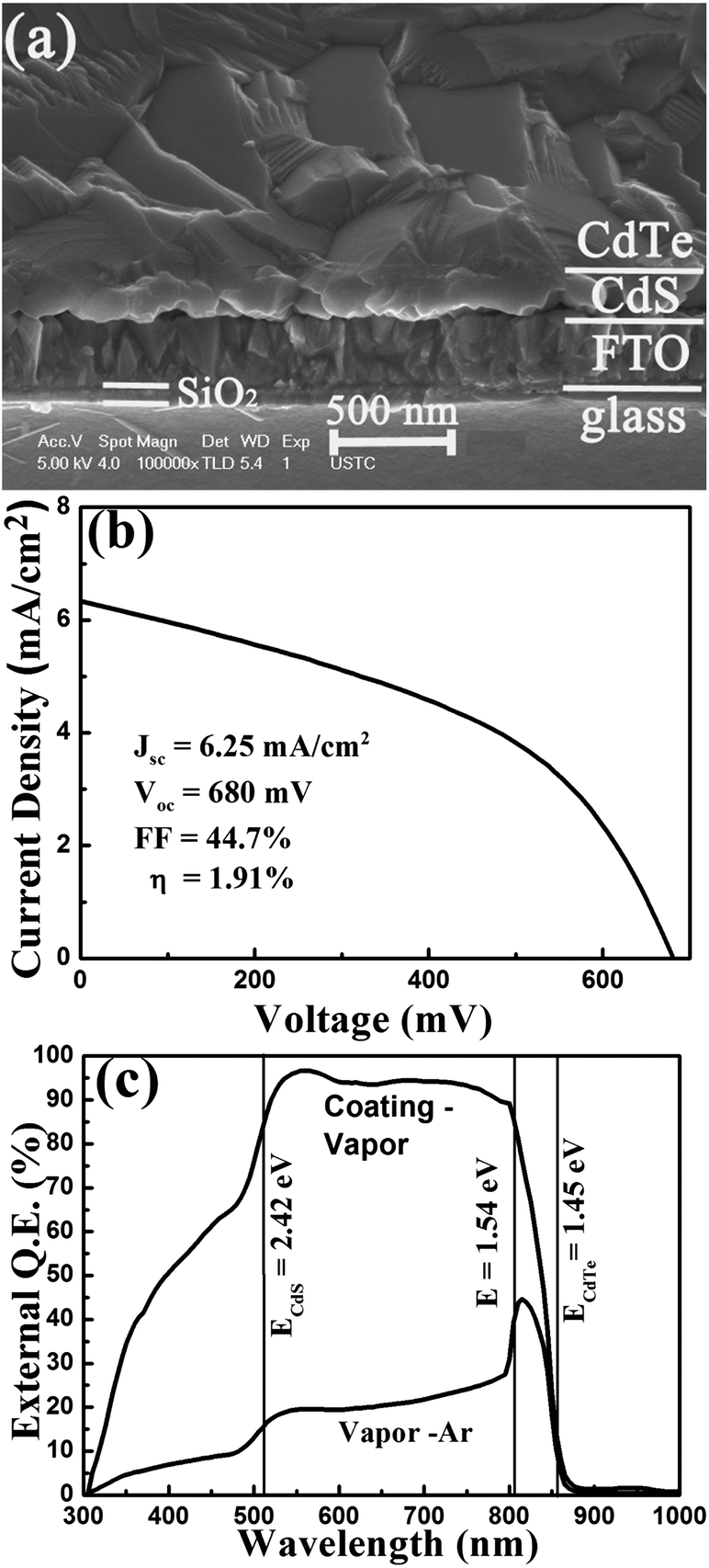 | ||
| Fig. 7 (a) SEM cross-sectional microstructure of a CdTe/CdS cell junction with an Ar-treated CdS window layer; (b) light current–voltage curve of the CdTe solar cell shown in (a); (c) external quantum efficiencies of two CdTe cells with an Ar-treated CdS and a coating-vapor CdS window layers, respectively. | ||
The experimental results presented so far demonstrated that oxygen plays an important role in the recrystallization process for CdS precursor layers prepared by the CBD technique. Too much oxygen in the annealing atmosphere would lead to severe oxidation in CdS and too little oxygen would make a CdS layer vulnerable to react heavily with CdTe, leading to formation of a dead layer near the CdS/CdTe interface. Based on these observations and analysis, we designed the third kind of annealing process technique, namely, a CdS precursor layer was first coated with a CdCl2 layer by dipping in the same saturated CdCl2–methanol solution as that used for the dip-coating one and then it was heat treated in a chamber in a mixed atmosphere of CdCl2 vapor and air. Such a design allowed the CdS precursor layer to avoid over-oxidation while coalescence of nano-sized CdS grains could still be easily achieved. Finally, a CdS thin film with a mono-grained CdS layer with grain size up to 100–300 nm was obtained, as shown in Fig. 8(a). The CdS grains were densely packed along the CdS/FTO interface and had well-defined crystalline facets. The most important thing to report is that the CdS grains showed a much better chemical stoichiometry as discussed in the following XPS results. These characteristics made it possible to reduce the CdS window layer thickness to several tens of nanometers for CdTe solar cell fabrication. XRD showed that the H(103) peak of the coating-vapor CdS was stronger than that of the dip-coating one and it showed a narrow peak at 28.3° corresponding to the H(101). As discussed above, electric shunting/shorting paths could be easily formed at the CdS/CdTe junction if a dip-coating CdS was employed as the window layer. The CdS/CdTe interface formed with the coating-vapor CdS film, seen in Fig. 8(b), showed an almost perfect junction with uniform CdS thickness. Pinholes were not observed at all along the CdS/CdTe interface. At such a mono-grain-CdS/CdTe junction, electrons transporting from the CdTe absorber to the front electrode FTO only need to go through one CdS grain without encountering any grain boundaries within the CdS layer.
 | ||
| Fig. 8 (a) SEM cross-sectional morphology of a CdS film after CdCl2 annealing by the coating-vapor method; (b) microstructure of a CdTe/CdS cell junction prepared with a coating-vapor CdS window layer. | ||
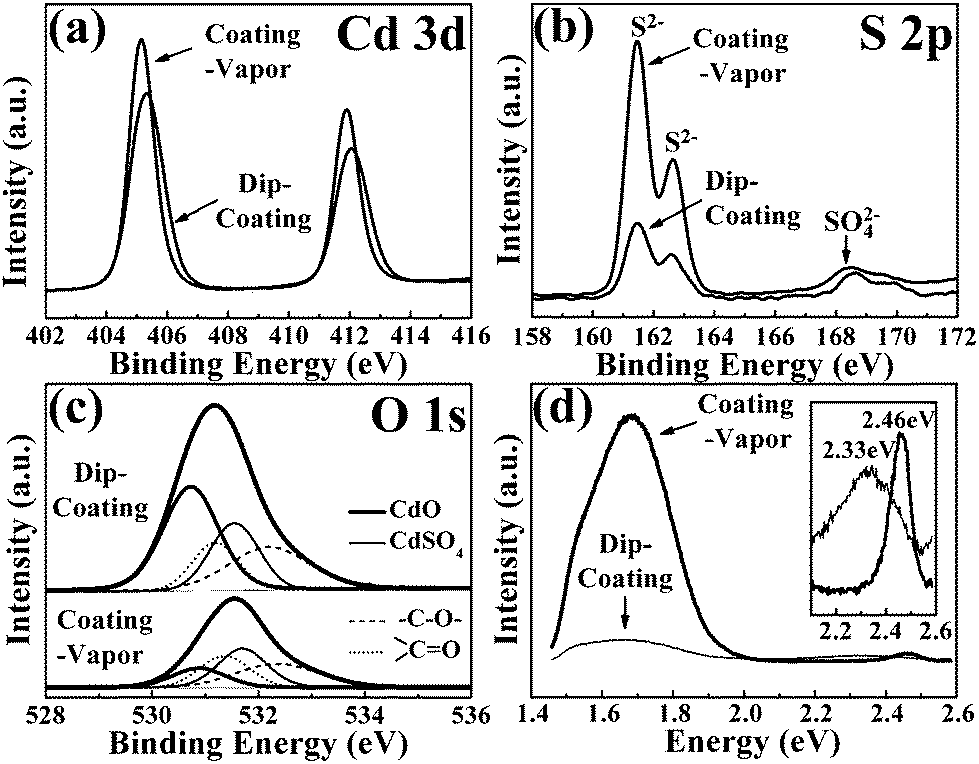
The CdS film surface chemical states were analyzed via high-resolution XPS spectra. For comparison, the intensity of XPS spectra was normalized for the two kinds of CdS films, namely a dip-coating and a coating-vapor CdS film. The results of the Cd 3d and S 2p peaks are shown in Fig. 9(a) and (b), respectively. Special attention was paid to the oxidation of the heat-treated CdS films. The binding energies of the Cd 3d in CdO and CdS are so close that it was difficult to fit the peaks with convincing fitting results. Therefore, for the study of film oxidation during the heat treatment the O 1s peak was fitted carefully as shown in Fig. 9(c). The Cd 3d spectrum of the dip-coating CdS showed a much broader peak with a slightly higher binding energy compared to that of the coating-vapor CdS, indicating that Cd in the dip-coating CdS had more non-uniform chemical binding states. The asymmetric O 1s peak in Fig. 9(c) indicates that near the CdS film surface multi-state oxidation occurred. The single and double bonding between C and O, which came from the absorbed molecules, have been routinely observed in our samples. For the dip-coating CdS, the main contribution to the O 1s peak came from the oxide CdO and CdSO4, while for the coating-vapor one, the O 1s intensity from the CdO was considerably lower. The XPS peak related to SO42− was unavoidable when a CdS film was prepared by the CBD method. In both samples, the O 1s contribution from the CdSO4, centered at 531.7 eV,11 was observed. The S 2p peak from SO42− was also observed in the S 2p spectrum shown in Fig. 9(b). The XPS results clearly demonstrated that the dip-coating CdS layer had been more severely oxidized, which is consistent with the XRD spectra shown in Fig. 3(d). The ratio of Cd from CdO to the total Cd measured by the XPS data was 61.9 ± 0.5% for the dip-coating CdS, while for the coating-vapor CdS, it was only 11.7 ± 0.5%. The atomic ratios of S/Cd were 30.2 ± 0.5% and 74.3 ± 0.5% for the dip-coating and coating-vapor CdS, respectively. The large sulfur deficiency was caused by loss of S atoms and substitution of the lattice S by the O atom.
 | ||
| Fig. 9 XPS survey spectra of CdS films prepared by the dip-coating and the coating-vapor method; (a) Cd 3d peak; (b) S 2p peak; (c) O 1s peak. (d) Room-temperature photoluminescence spectra for the two kinds of CdS films. | ||
Photoluminescence (PL) measurement was carried out at room temperature. The as-grown CdS film showed only very weak luminescence. Fig. 9(d) shows the photoluminescence spectra of the two kinds of CdS films after heat treatment. The dramatic difference is that the PL intensity of the coating-vapor CdS was much stronger, about 11 times higher than that of the dip-coating CdS. Two factors contributed to the increased PL intensity, namely, the higher crystalline quality and the much reduced density of defects located at the grain surface and boundaries, and in the interior of the CdS grains. The density of deep electronic states, which could quench the photoluminescence, was effectively reduced in the coating-vapor CdS. Near the band gap energy, the coating-vapor CdS showed a peak centered at 2.46 eV with a narrow full width at half maximum of only 0.086 mV, as shown in the inset of Fig. 9(d). The energy, 2.46 eV, is slightly higher than the band gap of hexagonal CdS measured at room temperature (2.42 eV),12 suggesting that this narrow peak can be attributed to bound excitons.13,14 The broad peak with energy of 1.5–1.8 eV was originated from point defects and their complexes. Detailed fittings (not shown here) indicated that the main contribution to this peak was related to the sulfur vacancy (∼1.71 eV).14,15
Investigation of the early stage in CdS recrystallization during the CdCl2 heat treatment was done to help us understand the recrystallization mechanism of the two different heat treatments. We heat treated two CdS precursor layers at a relatively low temperature of 310 °C. The SEM microstructures for the two samples after heat treatment are shown in Fig. 10. Fig. 10(a) and (c) present the surface and cross-sectional morphologies of the CdS film heat treated with the dip-coating method, while Fig. 10(b) and (d) show the corresponding microstructures of the film treated with the coating-vapor method. The figure parts clearly demonstrate that the coating-vapor CdS layer, compared to the dip-coating one, showed much larger grains with sizes as large as ∼100 nm and grains with well-defined facets that had begun to develop. It has been reported that for a CdS film prepared by CBD the phase transition from cubic to hexagonal began to occur at ∼300 °C.16 At this temperature the atoms in CdS gained relatively greater energy to move around to coalesce. The presence of the CdCl2 vapor enhanced the recrystallization process. Our previous study and in situ X-ray diffraction study reported by Kim et al.18 showed that when CdTe was coated with a CdCl2 layer, a low-melting eutectic mixture of CdTe–CdCl2 was formed, which assisted the CdTe recrystallization.17,18 Due to the chemical similarity of CdTe and CdS, we suggested that the CdCl2 coating layer and the presence of a CdCl2 vapor made it possible to form a low-melting mixture of CdS–CdCl2 at the CdS film surface, which assisted the recrystallization and grain growth. In-plane compressive or tensile stress may be developed in the film, assisting grain growth/coalescence with a preferred direction along the CdS/FTO interface.18 More detailed recrystallization mechanisms should be studied in the future. Without the presence of a CdCl2 vapor during the heat treatment, the dip-coating CdS layer had much smaller grains as shown in Fig. 10(a). This was caused by the incorporation of too much oxygen as discussed above. Raman scattering of the two CdS films showed spectral peaks with exactly the same Raman spectra. In situ and out situ Raman scattering experiments showed that the incorporation of O atoms, which were bonded with S and Cd atoms in the form of Os or Oi to form CdS1−xOx and CdO, were not sufficient to influence the Cd–S bonding in the CdS films. Based on these results we suggest that the oxides were formed mainly on the CdS grain surface and at the grain boundary.
 | ||
| Fig. 10 (a and b) SEM surface morphology, and (c and d) SEM cross-sectional morphology of the CdS films heat treated at 310 °C by the dip-coating and coating-vapor method, respectively. | ||
It is clear that the XPS data correlated well with the SEM microstructures and the XRD data shown in Fig. 3 and 6. For the dip-coating CdS, there were not enough Cl elements to prevent in a timely fashion the occupation of sulfur vacancy and substitution of the lattice S atoms by the oxygen, leading to oxidation on the CdS grain surface. This in turn blocked the coalescence of the relatively small-sized CdS grains. On the other hand, for the coating-vapor CdS, the CdCl2 coating layer and a high CdCl2 vapor pressure helped to prevent the incorporation of too much oxygen and ensured a homogenous and rapid recrystallization of the CdS film. The severe sulfur deficiency also hindered grain coalescence during the heat treatment. For the Ar-treated CdS, the absence of oxygen on the CdS grain surface enhanced the interdiffusion/reaction at the CdS/CdTe interface, and too much mixing between these two materials led to the formation of a dead layer as discussed above.
CdTe solar cells were fabricated on glass/FTO/CdS templates with the three different kinds of CdS window layers. Fig. 11 shows comparative device performance of CdTe solar cells using dip-coating and coating vapor CdS as window layers. As discussed above, if a CdS window layer made by the dip-coating method is thinner than ∼100 nm, it is easy to form shunting/shorting paths at the CdS/CdTe interface. In order to avoid shunting/shorting path formation and obtain high-efficiency solar cells, two cells employed dip-coating CdS films of 160 nm and 80 nm thickness as the window layers, while the cell that employed a coating-vapor CdS had a thickness of only 80 nm. The device properties of these solar cells are comparably shown in Fig. 11 and 12. If shunting paths were formed at the CdS/CdTe interface, even not seriously, the dark current–voltage curve of the diode would show a rather deteriorated characteristic. The shunting path dramatically reduces shunt resistance and increases the leakage current as shown in Fig. 11(a). The curve denoted as “cell with shunt path” was obtained from a cell with an 80 nm-thick CdS film prepared by the dip-coating method. The current density of the shunted cell increased approximately linearly with increased reverse-bias voltage. At low forward-bias voltage, the current flowing through the shunt resistance, which was linearly proportional to the voltage, was the major part of the total current. In order to get high-efficiency solar cells, we found that the thickness of the CdS layer, if prepared by the dip-coating method, must be at least double that of CdS layers prepared by the coating-vapor method. The log![[thin space (1/6-em)]](https://www.rsc.org/images/entities/char_2009.gif) J–V curves of the corresponding J–V curves are shown in Fig. 11(b). The reverse saturation currents were obtained by the intercept of the dashed lines with the y-axis at the zero voltage. The ideal quality factors of the p–n junctions were obtained by the slopes of the dashed fitting lines. The cell with a mono-grained, 80 nm-thick CdS had a very low reverse saturation current J0 on the order of ∼10−10 A cm−2 and a diode quality factor of 1.61 for the CdS/CdTe junction. Both of these values are difficult to attain for a CdTe cell owing to the polycrystalline nature of both the CdS and the CdTe films. The cell with the 160 nm-thick, dip-coating CdS had a higher J0 of ∼10−9 A cm−2 and the diode quality factor was 1.98, indicating that the current transport was dominated by mid- and/or deep-gap states at the junction.19,20 Obviously the high crystalline quality of the mono-grained CdS film ensured homogenous intermixing of CdS and CdTe at the interface and the density of gap states was decreased at the junction, resulting in a low ideality factor. An ideality factor of 1.54 was reported for a 15%-efficiency CdTe solar cell.20 The series and shunt resistance for the two cells with the mono-grained and the 160 nm-thick CdS were 3.3 and 6.3 Ω cm−2, and 716 and 718 Ω cm−2, respectively. The current–voltage characteristics of the two cells measured at AM 1.5 condition are shown in Fig. 11(c), and the corresponding efficiencies are 14.6 and 8.9%, respectively. The CdTe solar cell with the 80 nm-thick coating-vapor CdS window layer had a short-circuit current Jsc of 25.1 mA cm−2, which is comparable to that of the world-record-efficiency cell (25.9 mA cm−2).6 This high Jsc was ascribed to the high quality of the p–n junction and the much reduced thickness of the mono-grained CdS window layer, which allowed more light to transmit through the window layer to the CdTe absorber. This was clearly demonstrated by the EQE measurements shown in Fig. 11(d). With an 80 nm-thick CdS window layer, the EQE was improved in the wavelength range from 300 to 800 nm, especially in the short wavelength range from 300 to 500 nm. In this wavelength range, the photon energy is higher than the CdS band gap energy, causing a considerable absorption in the 160 nm-thick CdS window layer. In comparison, the Jsc increase of 6 mA cm−2 for the cell with the mono-grained CdS was well correlated with an overall EQE improvement of about 30%.
J–V curves of the corresponding J–V curves are shown in Fig. 11(b). The reverse saturation currents were obtained by the intercept of the dashed lines with the y-axis at the zero voltage. The ideal quality factors of the p–n junctions were obtained by the slopes of the dashed fitting lines. The cell with a mono-grained, 80 nm-thick CdS had a very low reverse saturation current J0 on the order of ∼10−10 A cm−2 and a diode quality factor of 1.61 for the CdS/CdTe junction. Both of these values are difficult to attain for a CdTe cell owing to the polycrystalline nature of both the CdS and the CdTe films. The cell with the 160 nm-thick, dip-coating CdS had a higher J0 of ∼10−9 A cm−2 and the diode quality factor was 1.98, indicating that the current transport was dominated by mid- and/or deep-gap states at the junction.19,20 Obviously the high crystalline quality of the mono-grained CdS film ensured homogenous intermixing of CdS and CdTe at the interface and the density of gap states was decreased at the junction, resulting in a low ideality factor. An ideality factor of 1.54 was reported for a 15%-efficiency CdTe solar cell.20 The series and shunt resistance for the two cells with the mono-grained and the 160 nm-thick CdS were 3.3 and 6.3 Ω cm−2, and 716 and 718 Ω cm−2, respectively. The current–voltage characteristics of the two cells measured at AM 1.5 condition are shown in Fig. 11(c), and the corresponding efficiencies are 14.6 and 8.9%, respectively. The CdTe solar cell with the 80 nm-thick coating-vapor CdS window layer had a short-circuit current Jsc of 25.1 mA cm−2, which is comparable to that of the world-record-efficiency cell (25.9 mA cm−2).6 This high Jsc was ascribed to the high quality of the p–n junction and the much reduced thickness of the mono-grained CdS window layer, which allowed more light to transmit through the window layer to the CdTe absorber. This was clearly demonstrated by the EQE measurements shown in Fig. 11(d). With an 80 nm-thick CdS window layer, the EQE was improved in the wavelength range from 300 to 800 nm, especially in the short wavelength range from 300 to 500 nm. In this wavelength range, the photon energy is higher than the CdS band gap energy, causing a considerable absorption in the 160 nm-thick CdS window layer. In comparison, the Jsc increase of 6 mA cm−2 for the cell with the mono-grained CdS was well correlated with an overall EQE improvement of about 30%.
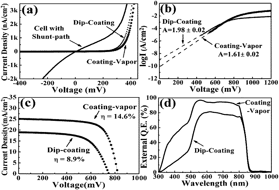 | ||
| Fig. 11 (a) Dark current–voltage curves for CdTe solar cells with different kinds of CdS window layers as described in the text; (b) log curves of the dark current–voltage data; (c) light current–voltage characteristics measured at AM 1.5 condition; (d) external quantum efficiencies of two CdTe cells with window layers of 160 nm thick for the dip-coating CdS and of 80 nm thick for the coating-vapor CdS, respectively. | ||
 | ||
| Fig. 12 Comparative external quantum efficiencies for the two CdTe solar cells having 80 nm-thick CdS window layers prepared by the dip-coating and coating-vapor methods, respectively. | ||
We also prepared solar cells with the two kinds of CdS having the same thickness of 80 nm, and the comparative EQEs are shown in Fig. 12. Both cells showed much increased EQE in the wavelength range of ∼300–517 nm due to the reduced photon absorption in the thin CdS window layers. The short wavelength photons were mostly absorbed in CdTe near the junction and the carriers were efficiently separated due to the relatively strong electric field at the CdTe/CdS junction, leading to almost the same EQE for both cells; even the cell with a dip-coating CdS had shunting paths at the junction. However, for wavelengths greater than ∼517 nm, the solar cell with the dip-coating CdS window layer showed a much reduced EQE from ∼517 to 850 nm. Photons with longer wavelengths were absorbed deep in the CdTe away from the p–n junction as discussed for the cell with an Ar-treated CdS window layer. Due to the formation of pinholes at the junction, the electric field was weaker because of the reduced junction area, which led to enhanced recombination for carriers generated deep in the CdTe.21 Thus a much reduced EQE was measured for the solar cell with a dip-coating CdS window layer.
4. Conclusions
In conclusion, the experimental results presented in this study demonstrate that the presence of a certain concentration of oxygen during the re-crystallization of a CdS precursor layer was important to control the CdS grain coalescence, surface chemical stoichiometry, and interdiffusion between CdS and CdTe. Coating a CdS precursor film with a CdCl2 layer and heat treating in a high CdCl2 vapor pressure atmosphere helped to reduce over-oxidation at grain surfaces/boundaries and promoted in-plane grain coalescence along the CdS/FTO interface. High crystalline CdS films with only one mono-grained layer with a thickness of several tens of nanometers were successfully obtained and employed as window layers to fabricate highly efficient CdTe solar cells. Homogenous and controllable intermixing of CdS and CdTe at the CdS/CdTe interface was achieved. CdTe solar cell with an efficiency of 14.6% was fabricated. Lack of oxygen in CdS during the re-crystallization process, although it led to easy coalescence of nano-sized CdS grains and formation of CdS films with large grains, induced too much interdiffusion/reaction at the CdS/CdTe interface.Acknowledgements
This work was financially supported by the National Natural Science Foundation of China (no. 51272247 and 60976054).Notes and references
- B. E. McCandless and K. D. Dobson, Sol. Energy, 2004, 77, 839 CrossRef CAS PubMed.
- Z. Bai, J. Yang and D. Wang, Appl. Phys. Lett., 2011, 99, 143502 CrossRef PubMed.
- D. Wang, Z. Hou and Z. Bai, J. Mater. Res., 2011, 26, 697 CrossRef CAS.
- A. Bosio, N. Romeo, S. Mazzamuto and V. Canevari, Prog. Cryst. Growth Charact. Mater., 2006, 52, 247 CrossRef CAS PubMed.
- T. M. Razykov, C. S. Ferekides, D. Morel, E. Stefanakos, H. S. Ullald and H. M. Upadhyaya, Sol. Energy, 2011, 85, 1580 CrossRef CAS PubMed.
- X. Wu, Sol. Energy, 2004, 77, 803 CrossRef CAS PubMed.
- A. Rios-Flores, J. L. Peña, V. Castro-Peña, O. Ares, R. Castro-Rodríguez and A. Bosio, Sol. Energy, 2010, 84, 1020 CrossRef CAS PubMed.
- D. S. Albin, Y. Yan and M. M. Al-Jassim, Prog. Photovolt: Res. Appl., 2002, 10, 309 CrossRef CAS.
- X. Mathew, J. S. Cruz, D. R. Coronado, A. R. Millán, G. C. Segura, E. R. Morales, O. S. Martínez, C. C. Garcia and E. P. Landa, Sol. Energy, 2012, 85, 1580 Search PubMed.
- J. P. Enriquez and X. Mathew, Sol. Energy Mater. Sol. Cells, 2003, 76, 313 CrossRef CAS.
- J. Riga, J. J. Verbist, P. Josseaux and A. K. Mesmaeker, Surf. Interface Anal., 1985, 7, 163 CrossRef CAS.
- B. Ray, II-VI Compounds, Oxford, Pergamon, 1969 Search PubMed.
- J. Aguilar-Hernandez, J. Sastre-Hernandez, R. Mendoza-Perez, M. Cardenas-Garcia and G. Contreras-Puente, Phys. Status Solidi C, 2005, 2, 3710 CrossRef CAS.
- J. Aguilar-Hernandez, J. Sastre-Hernandez, R. Mendoza-Perez, G. Contreras-Puente, M. Cardenas-Garcia and J. Ortiz-Lopez, Sol. Energy Mater. Sol. Cells, 2006, 90, 704 CrossRef CAS PubMed.
- J. N. Ximello-Quiebras, G. Contreras-Puente, J. Aguilar-Hernandez, G. Santana-Rodriguez and A. Carbajal-Readigos, Sol. Energy Mater. Sol. Cells, 2004, 82, 263 CrossRef CAS PubMed.
- O. Zelaya-Angel and R. Lozada-Morales, Phys. Rev. B: Condens. Matter Mater. Phys., 2000, 62, 13064 CrossRef CAS.
- Z. Bai and D. Wang, Phys. Status Solidi A, 2012, 209, 1982 CrossRef CAS.
- M. J. Kim, J. J. Lee, S. H. Lee and S. H. Sohn, Sol. Energy Mater. Sol. Cells, 2012, 109, 209 CrossRef PubMed.
- S. S. Hegedus and B. E. McCandless, Sol. Energy Mater. Sol. Cells, 2005, 88, 75 CrossRef CAS PubMed.
- D. M. Oman, K. M. Dugan, J. L. Killina, V. Ceekala, C. S. Ferekides and D. L. Morel, Sol. Energy Mater. Sol. Cells, 1999, 58, 361 CrossRef CAS.
- K. Ernst, R. Engelhardt, K. Ellmer, C. Kelch, H.-J. Muffler, M.-Ch. Lux-Steiner and R. Könenkamp, Thin Solid Films, 2001, 387, 26 CrossRef CAS.
| This journal is © The Royal Society of Chemistry 2014 |