Growth of γ-Fe2O3 nanosheet arrays on graphene for electromagnetic absorption applications†
Yulan Rena,
Chunling Zhu*a,
Lihong Qib,
Hong Gaoc and
Yujin Chen*b
aKey Laboratory Superlight Materials and Surface Technology, Ministry of Education, College of Materials Science and Chemical Engineering, Harbin Engineering University, Harbin, Heilongjiang 150001, China. E-mail: zhuchunling@hrbeu.edu.cn; Tel: +86-451-82519754
bCollege of Science, Harbin Engineering University, Harbin 150001, China. E-mail: chenyujin@hrbeu.edu.cn; Fax: +86-451-82519754; Tel: +86-451-82519754
cKey Laboratory for Photonic and Electric Bandgap Materials, Ministry of Education, Harbin Normal University, Harbin, 150025, P.R. China
First published on 23rd April 2014
Abstract
We developed a seed-assisted method to grow ultra-thin γ-Fe2O3 nanosheets with a paramagnetic behaviour on the surfaces of graphene sheets. Scanning electron microscopy and the transmission electron microscopy measurements showed that the length, height and thickness of the nanosheets were about 140, 120 and 5 nm, respectively. The measured electromagnetic parameters indicated that the three-dimensional (3D) graphene/γ-Fe2O3 nanosheet arrays exhibited a significantly enhanced electromagnetic wave absorption property compared to that of the graphene sheets and some magnetic nanomaterials. The minimal reflection loss was less than −15.2 dB for 3D graphene/γ-Fe2O3 nanosheet arrays with thicknesses of 2 mm, and it was up to −64.1 dB when the thickness was 4.92 mm. Good electromagnetic wave absorption properties of the 3D graphene/γ-Fe2O3 nanosheet arrays indicate that they are very promising for applications in the electromagnetic wave absorbing field.
1 Introduction
Heteronanostructures have drawn unique attention in nanoscience because it is difficult for a single component material to offer corresponding exceptional properties and multifunctionality. Graphene (G) has excellent mechanical, electrical, thermal and optical properties together with an ultrathin effective 2D structure. Furthermore, graphene can incorporate abundant oxygen functional groups such as –OH and –C![[double bond, length as m-dash]](https://www.rsc.org/images/entities/char_e001.gif) O on its surface. These properties make it an ideal substrate for the deposition and/or growth of other functional materials. Recently, various G-based heteronanostructures have been fabricated, extending the application of graphene into new fields such as energy storage and conversion, chemical catalysts and optoelectronic devices and sensors.1–17
O on its surface. These properties make it an ideal substrate for the deposition and/or growth of other functional materials. Recently, various G-based heteronanostructures have been fabricated, extending the application of graphene into new fields such as energy storage and conversion, chemical catalysts and optoelectronic devices and sensors.1–17
Among these materials, magnetic graphene heteronanostructures have many potential applications such as contrast enhancement agents in magnetic resonance imaging, energy storage, electromagnetic (EM) wave absorption, etc.4–13 For example, G/Fe3O4 heteronanostructures with superparamagnetic, conductive and multifunctional properties show great promise as materials for magnetic resonance imaging.4 Very recently, highly ordered 3D G-based heteronanostructures with high specific surface area, a large number of active sites and superior mechanical strength have been synthesized. Because of their unique geometry, these 3D heteronanostructures are being considered for applications in optoelectronic devices, catalysts and lithium ion batteries.15,17,18 However, growth of magnetic nanosheet arrays on the surfaces of graphene sheets has rarely been reported.
EM wave-absorbing materials have attracted a great deal of attention because of increasing EM interference and radiation problems. For these applications, lightweight materials with strong absorption properties are required. To meet these requirements, researchers have recently developed various methods to fabricate nanostructures for use in lightweight EM absorbers.19–31 Heteronanostructured materials exhibit strong EM absorption properties because of interfacial and synergistic effects. For example, the reflection losses for EM waves reached −25 dB for carbon nanotube/Fe core/shell nanostructures with a thickness of 1.2 mm,21 and −30 dB for Fe3O4/ZnO core/shell nanorods with a thickness of 1.5 mm.27 However, the amount of absorbers added to the paraffin matrix need to be decreased significantly for practical applications.
Graphene, representative of a new class of 2D carbonaceous materials, is a very promising candidate for a lightweight EM absorber. However, its high conductivity, which would lead to its poor EM absorption ability, is a serious drawback.32–34 This drawback can be overcome to some extent by designing G-based heteronanostructures in which dielectric or magnetic loss nanostructured materials are deposited on the surface of the graphene sheets.6–12,18 The fabrication of G-based heteronanostructures using a rational design process may be an efficient strategy for obtaining EM absorbers that are both lightweight and have strong absorption properties.
Very recently, we developed a new seed-assisted method for fabricating a combination 3D G/SiO2@Fe3O4 core/shell nanorod array architecture.35 In this work, we fabricated 3D G/γ-Fe2O3 nanosheet array (NSA) heteronanostructures by a modification of the abovementioned method. Three steps were involved in the formation of the 3D G/γ-Fe2O3 NSAs, as shown in Fig. 1. The graphene sheets were first dispersed in a ferric nitrate aqueous solution to grow β-FeOOH nanostructures on their surfaces (step 1 in Fig. 1).6,8 These nanostructures served as “seeds” for the growth of β-FeOOH NSAs on the surfaces of graphene sheets in a ferric chloride aqueous solution under a hydrothermal condition (step 2 in Fig. 1). Finally, the 3D G/γ-Fe2O3 NSAs were obtained after a thermal treatment of the G/β-FeOOH NSAs (step 3 in Fig. 1). Because of their special morphology, the 3D G/γ-Fe2O3 NSA heterostructures exhibited very good properties, including strong attenuation of EM waves and low device mass.
 | ||
| Fig. 1 Growth processes of 3D G/γ-Fe2O3 NSAs. | ||
2 Experimental section
2.1. Materials
The graphene sheets used in this work were purchased from Nanjing XFNano Material Tech Co., Ltd. (Nanjing City, China). Their thickness and specific surface area are about 0.8 nm and 500–600 m2 g−1, respectively, and the corresponding oxygen content is about 7 wt%. Their synthesis is as follows: graphite oxide (GO) was prepared from natural graphite using a modified Hummers method. The GO was then thermally treated at a high temperature under an N2 flow, and finally reduced at 1200 °C under an H2 atmosphere. All the other reagents were analytically pure and used without further purification.2.2. Synthesis of G/β-FeOOH NSAs
The 3D G/γ-Fe2O3 NSAs were fabricated by a seed-assisted method, as illustrated in Fig. 1. First, 0.01 g of graphene sheet was dispersed into 300 mL water with ultrasonication, and then 1.0 g of Fe(NO3)3·9H2O was added. This mixture was stirred at 50 °C for 2 h. The precipitates were then separated by centrifugation, washed with distilled water and pure ethanol and then vacuum-dried. Next, 15 mg of the precipitate was dispersed in 35 mL of a solution containing 0.5 g FeCl3·6H2O and 1.0 g sodium nitrate, and this mixture was stirred for 20 min. This mixture was then transferred into a Teflon-lined stainless steel autoclave (capacity of 50 mL) for hydrothermal treatment at 60 °C for 12 h. After the autoclave cooled down to room temperature naturally, the precipitates were separated by centrifugation, washed with distilled water and pure ethanol and dried in air.2.3. Synthesis of G/γ-Fe2O3 NSAs
The final G/γ-Fe2O3 NSAs were fabricated by thermal treatment of the G/β-FeOOH NSAs at 300 °C for 2 h in air.2.4 Structural characterization
The morphology and size characteristics of the synthesized samples were characterized using a Hitachi S-5200 scanning electron microscope (SEM) and an FEI Tecnai-F20 transmission electron microscope (TEM) equipped with a Gatan imaging filter (GIF). The operating voltages of SEM and TEM were 5 kV and 200 kV, respectively. The crystal structure of the sample was determined by X-ray diffraction (XRD) using a Rigaku D/max 2550 V diffractometer and Cu Kα radiation. X-ray photoelectron spectroscopy (XPS) measurements were carried out using a PHI 5700 ESCA spectrometer with Al Kα radiation. Raman spectrum was collected on a HR Jobin Yvon spectrometer. The magnetic properties of the hierarchical 3D G/γ-Fe2O3 NSA material were measured using vibrating sample magnetometry (VSM).2.5. EM parameter measurements
The EM properties of the samples were measured using the transmission/refection coaxial line method. The measurement setup consisted of an ANRITSU 37269D vector network analyzer with a synthesized sweep oscillator source and an S-parameter test set. The measured samples were prepared by uniformly mixing 20 wt% of the sample in a paraffin matrix. The mixture was then pressed into toroidal samples (φout: 7.00 mm; φin: 3.04 mm).3 Results and discussion
3.1. Growth of β-FeOOH seeds on the surfaces of the graphene sheets
It is well known that amorphous Fe(OH)3 colloidal nanoparticles can be produced during the hydrolysis of ferric nitrate.36,37 If the template materials are dispersed in the ferric nitrate solution prior to hydrolysis, the colloidal nanoparticles will be deposited on the template surfaces.6,8,36–39 The hydrolysis conditions (time and temperature) and the type of template material have an influence on the morphology and crystalline phase of the final deposited product. For example, amorphous Fe(OH)3 particles would be produced on the surface of α-MoO3 nanorods at a hydrolysis temperature of 50 °C,38,39 whereas β-FeOOH nanocrystals would be formed on the surfaces of the graphene sheets under the same conditions.6,8,40 Under the present experimental conditions, β-FeOOH nanostructures with different morphologies grow on the surfaces of the graphene sheets. As shown in Fig. 2(a), aside from a few small nanoparticles, many nanosheets with a length of about 150 nm grew on the graphene. A typical low-resolution TEM image (Fig. 2(b)) indicates that the diameter of the small β-FeOOH particles and the thicknesses of the β-FeOOH nanosheets are less than 5 nm and 8 nm, respectively. Distinct lattice fringes are observed in the high-resolution TEM (HRTEM) images (insets in Fig. 2(c) and (d)), suggesting that both the nanoparticles and nanosheets are crystalline. Fig. 2(e) shows the selected area electron diffraction (SAED) pattern of the composites. The labelled diffraction rings in the pattern correspond to the (200), (101), (301) and (600) planes of orthorhombic β-FeOOH (JCPDS card number 75-1594, cell parameters: a = 8.40 Å and c = 3.0 Å). These results reveal that β-FeOOH nanocrystals, including nanoparticles and nanosheets, were grown on the surfaces of the graphene sheets.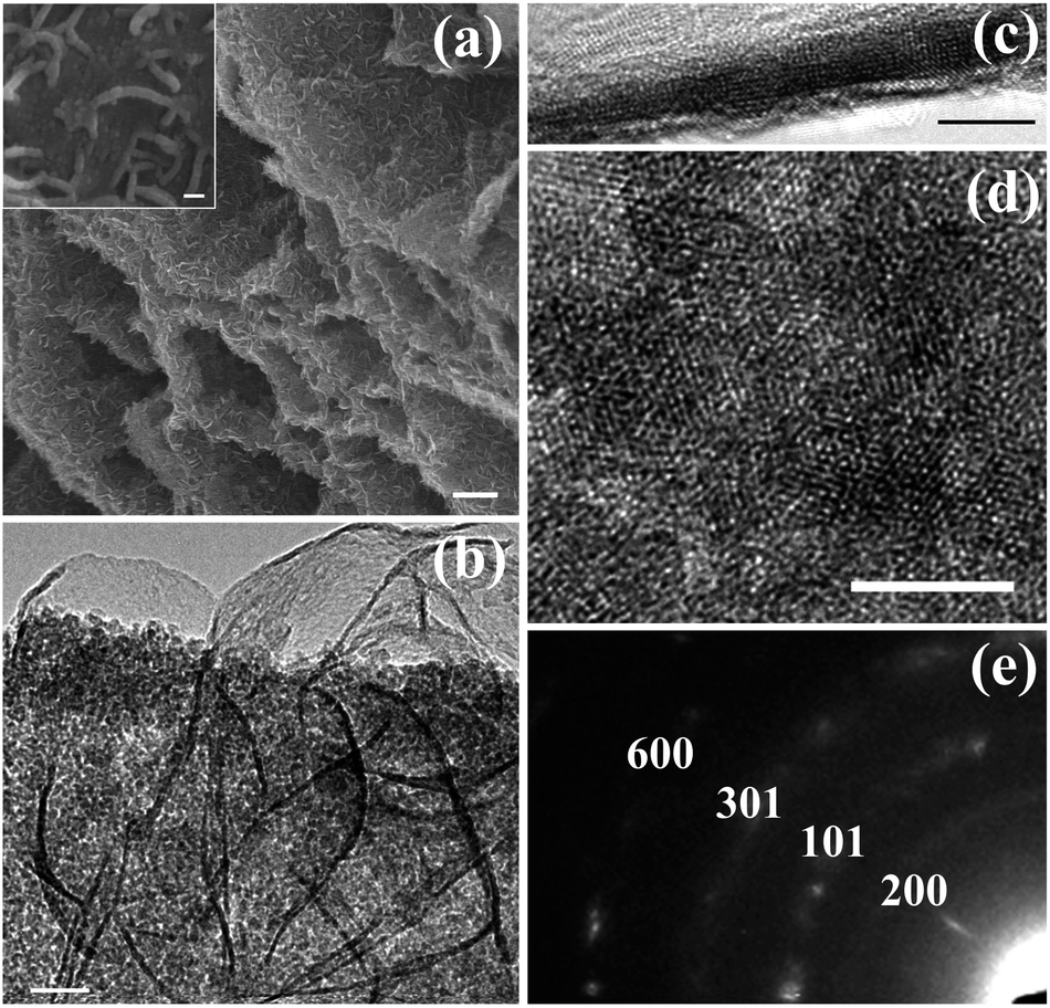 | ||
| Fig. 2 Structural characterizations of β-FeOOH seed/G composites. (a) SEM image, the inset shows a magnified SEM image, (b) TEM image, (c) HRTEM image for β-FeOOH nanosheets, (d) HRTEM image for β-FeOOH nanoparticles, and (e) SAED pattern. Scale bar: (a) 400 nm, and the inset images: 50 nm, (b) 20 nm and (c) and (d) 5 nm. | ||
3.2. Formation of G/β-FeOOH NSAs
All of the indexed diffraction peaks in the XRD pattern collected from the G/β-FeOOH NSA materials can be assigned to orthorhombic β-FeOOH crystals (Fig. S1, ESI†). Top-view SEM images, shown in Fig. 3(a) and the bottom inset, indicate that most of the β-FeOOH nanosheets with a typical length of about 180 nm are grown on the surfaces of the graphene sheets. The cross-sectional SEM image (top inset in Fig. 3(a)) clearly shows that β-FeOOH nanosheets with a height of about 130 nm grow on both sides of the graphene sheets, forming interesting 3D architectures. In the case where the β-FeOOH nanosheets are present on both side surfaces of the graphene sheets, the efficient stacking and aggregation of individual graphene sheets is impaired. | ||
| Fig. 3 Structural characterizations of the G/β-FeOOH nanosheet arrays. (a) Top-view SEM image, top-inset showing cross-section SEM image, and bottom-inset showing magnified top-view SEM image, (b) low-resolution TEM image, (c) HRTEM image for an individual β–FeOOH nanosheet and (d) SAED pattern. Scale bar: (a) 400 nm, and the inset images: 100 nm, (b) 1 μm and (c) 5 nm. | ||
The HRTEM image in Fig. 3(c) demonstrates that the β-FeOOH nanosheets have poor crystallinity. The SAED pattern in Fig. 3(d) confirms that β-FeOOH nanosheets are polycrystalline, and the labelled diffraction rings correspond to the (220), (101), (211), (411) and (620) crystalline planes of orthorhombic β-FeOOH. The β-FeOOH nanosheets grow more densely on the G surfaces than that have been hydrothermally treated. However, it should be noted that β-FeOOH NSAs will not be formed if the graphene sheets without β-FeOOH seeds are added in the reaction system (Fig. S2, ESI†). In this case, nanorods with nonuniform morphologies are irregularly deposited. Therefore, the presence of β-FeOOH seeds on the surfaces of graphene sheets plays a very important role in the formation of the nanosheet arrays.
3.3. Synthesis of 3D G/γ-Fe2O3 NSAs
It is apparent from the inset images in Fig. 4 that the 3D G/γ-Fe2O3 NSAs, when dispersed in water, can be manipulated by an external magnet. The field-dependent magnetization for the 3D G/γ-Fe2O3 NSAs was measured by a VSM at room temperature, as shown in Fig. 4. The magnetization hysteresis loop is sigmoidal, and the corresponding maximum saturation magnetization value is about 5.47 emu g−1. Since the coercivity and retentivity values are very close to zero, the 3D G/γ-Fe2O3 NSAs exhibits a paramagnetic behaviour. | ||
| Fig. 4 Magnetization hysteresis loop of the 3D G/γ-Fe2O3 NSAs, and photographs of the 3D G/magnetic NSAs dispersed in water before (top inset) and after (bottom inset) adding a magnet. | ||
All diffraction peaks indicated by Miller indices in the XRD pattern of G/γ-Fe2O3 NSAs can be indexed to cubic maghemite (JCPDS card number 39-1346, cell parameters: a = 8.35 Å) (Fig. S3, ESI†). In the Fe 2p core level XPS spectrum of the G/γ-Fe2O3 NSAs, there are the two main peaks located at 712.4 and 725.3 eV, corresponding to Fe 2p3/2 and Fe 2p1/2, respectively (Fig. S4, ESI†). The shakeup satellite peak (indicated by an arrow), which is the “fingerprint” of the specific electronic structure of iron oxides such as hematite or maghemite, can be identified.41 These results imply that the Fe3O4 phase is not present in the 3D G/γ-Fe2O3 NSAs. The Raman spectrum (Fig. S5†) shows the characteristic peaks of γ-Fe2O3 at 390, 490 and 589 cm−1, while the characteristic peak of magnetite at 668 cm−1 is not present.42† Thus, the XRD, Raman and XPS measurements demonstrate that the magnetic properties of the 3D G/γ-Fe2O3 NSAs can be attributed to the presence of γ-Fe2O3 in the nanostructures.
The morphology and structure of the 3D G/γ-Fe2O3 nanosheet heteronanostructures were further investigated by SEM and TEM measurements. A top-view SEM image, shown in Fig. 5(a), indicates that γ-Fe2O3 NSAs retained a similar morphology to that of the β-FeOOH NSAs (Fig. 3(a)). The height of the γ-Fe2O3 NSAs on the graphene sheets is about 120 nm (Fig. 5(a)). The inset in Fig. 5(a) is a magnified SEM image, showing that the length of the nanosheets is about 140 nm. The low-resolution and magnified TEM images (Fig. 5(b) and inset) demonstrate that the thickness of β-FeOOH nanosheets is about 5 nm. This reveals that although the 3D nanostructures are similar in overall morphology to those without thermal treatment, the length and the thickness of the nanosheets decreased slightly during thermal treatment. This is a result of the structural change of the orthorhombic β-FeOOH to maghemite and the loss of water. Clear lattice fringes are observed in an HRTEM image of the γ-Fe2O3 nanosheets (Fig. 5(c)), further confirming their crystalline nature. The labeled spacing in the image is about 0.252 nm, corresponding to (311) plane of cubic maghemite. The diffraction rings in the SAED pattern (Fig. 5(d)) correspond to (220), (221), (311), and (521) crystalline planes of cubic maghemite. The Bruanuer–Emmett–Teller (BET) surface area of the 3D G/γ-Fe2O3 NSAs was calculated to be 113.7 m2 g−1 in terms of the nitrogen adsorption–desorption isotherms (Fig. S6, ESI†). Collectively, the measurements presented above demonstrate that 3D G/γ-Fe2O3 NSAs with paramagnetic properties and high surface area can be fabricated by the seed method.
 | ||
| Fig. 5 Structural characterization of 3D G/γ-Fe2O3 NSAs. (a) SEM image, inset showing magnified top-view SEM image, (b) low-resolution TEM image, (c) HRTEM image for magnetic nanosheets and (d) SAED pattern. Scale bar: (a) 400 nm, and the inset image: 50 nm, (b) 200 nm, and the inset image: 20 nm and (c) 2 nm. | ||
3.4. EM absorption properties of 3D G/γ-Fe2O3 NSAs
The EM absorption properties of 3D G/γ-Fe2O3 NSAs were investigated for the relative complex permittivity (εr = ε′ − jε′′) and the relative complex permeability (μr = μ′ − jμ′′). Fig. 6(a) shows the frequency-dependent relative complex permittivity curves of the 3D G/γ-Fe2O3 NSAs. The real and the imaginary part vary in the range of 4.5–8.4 and 1.8–4.0, respectively, for the 3D G/γ-Fe2O3 NSAs in the frequency region of 2–18 GHz. The values of the dielectric loss tangent (tanδe = ε′′/ε′) of the 3D G/γ-Fe2O3 NSAs are 0.36–0.47 over 2–18 GHz (Fig. S7, ESI†). These values are significantly larger than those of the other magnetic materials.25,26 In addition, the dielectric tangent losses fluctuate little over the 2–18 GHz range, which demonstrates that the dielectric loss to EM waves of the 3D G/γ-Fe2O3 NSAs is not only strong, but also very stable over this frequency range. Fig. 6(b) shows the frequency-dependent relative complex permeability curves of the 3D G/γ-Fe2O3 NSAs. The values of the real part are in the range of 0.97–1.09. The weak resonance peak at about 2.0 GHz is similar to the behaviour of G/Fe3O4 nanohybrids.26 The maximum value of the magnetic loss tangent (tanδm = μ′′/μ′) of the 3D G/γ-Fe2O3 NSAs is 0.22, indicating that they present magnetic losses to EM waves (Fig. S7, ESI†).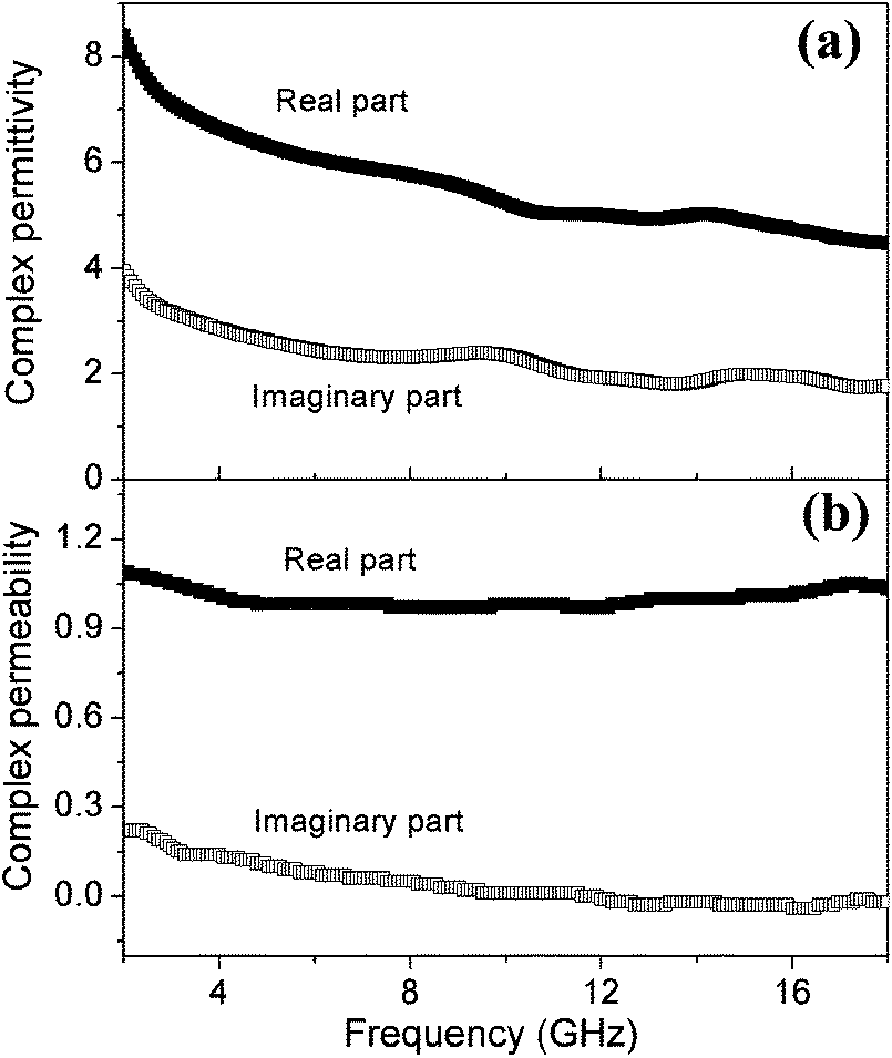 | ||
| Fig. 6 (a) The complex permittivity and (b) the complex permeability of the 3D G/γ-Fe2O3 NSAs. | ||
The 3D G/γ-Fe2O3 NSAs have strong and efficient dielectric loss over a 2–18 GHz frequency range, which, together with the magnetic loss at low frequencies, suggests that they have good EM absorption properties. The reflection loss (RL) values were calculated using the following equations at a given frequency and layer thickness according to the transmission line theory:43
Zin = Z0(μr/εr)1/2![[thin space (1/6-em)]](https://www.rsc.org/images/entities/char_2009.gif) tanh[j(2πfd/c)(μrεr)1/2 tanh[j(2πfd/c)(μrεr)1/2
| (1) |
 | (2) |
In eqn (1) and (2), Z0 is the impedance of free space, Zin is the input characteristic impedance at the absorber/air interface, c is the velocity of EM waves in free space, f is the frequency of the microwaves and d is the thickness of the absorber.
The calculated reflection losses (RL) of the 3D G/γ-Fe2O3 NSAs are shown in Fig. 7. It can be found that the minimal RL values are less than −15.2 dB for the 3D G/γ-Fe2O3 NSAs with thicknesses of 2 mm, and this increases up to −64.1 dB at 6.48 GHz at a thickness of 4.92 mm. All the RL values for the graphene sheets are larger than −11 dB,8,17 indicating that the growth of the γ-Fe2O3 NSAs on the graphene sheets significantly enhanced their EM absorption properties. Compared with other magnetic materials, such as G/Fe3O4 nanohybrids6 and Fe3O4/TiO2 and Fe3O4/SnO2 core/shell nanostructures,25,28,34 the 3D G/γ-Fe2O3 NSAs exhibit very good EM absorption properties (Table 1). For example, the RL values of the Fe3O4/TiO2 core/shell nanotubes are larger than −20.6 dB when the thickness is in the range of 2–5 mm. Compared with other graphene-based magnetic materials such as G/Ni and G/Fe3O4 heteronanostructures, the 3D G/γ-Fe2O3 NSAs also exhibit better EM absorption properties, as shown in Table 1. Moreover, the added weight of these magnetic materials in the matrix is more than 40 wt% of the total.25,28 Thus, the 3D G/γ-Fe2O3 NSAs represent a lightweight alternative to other EM-absorbing materials.
 | ||
| Fig. 7 (a) The reflection losses of the 3D G/γ-Fe2O3 NSAs and (b) the top view of (a). | ||
| Materials | RL, min (dB) | C (wt%) | Reference |
|---|---|---|---|
| a C denotes the added amounts of the absorbents in the paraffin composites. | |||
| Fe3O4/ZnO | −30.0 | 50 | 27 |
| Fe3O4/TiO2 | −20.6 | 50 | 28 |
| Fe3O4/SnO2 | −27.4 | 80 | 25 |
| Fe3O4/C | −27.4 | 55 | 29 |
| Graphene | >−11.0 | 20 | 8 |
| G/Ni | −13.8 | 20 | 10 |
| G/Ni | −17.8 | 60 | 11 |
| G/Fe3O4 | −20.0 | 20 | 6b |
| G/γ-Fe2O3 | −61.4 | 20 | This work |
Recently, mechanisms such as zero reflection and geometrical effects have been proposed to interpret the EM absorption properties of these materials. For zero reflection, in terms of EM wave theory, the relationship μr = εr should be satisfied.22 However, the permittivity of 3D G/γ-Fe2O3 NSAs is much higher than their permeability. Therefore, the EM absorption properties of 3D G/γ-Fe2O3 NSAs are not explained by the zero reflection mechanism.
As for the geometrical effect, it occurs when the incident and reflected waves in the absorbers are out of phase by 180°. This effect is strongly dependent on the thickness (t) of absorbers according to44
| t = nλm/4 (n = 1, 3, 5, …), | (3) |
The excellent EM absorption performance of the G/γ-Fe2O3 NSAs should be related to their special structure and their synergetic effect. On one hand, the γ-Fe2O3 NSAs grown on both sides of the graphene sheets can decrease the resistance of the absorbers. The decreased resistivity (1/σ) will lead to an increase in the dielectric loss according to
| ε′′ ∝ σ/2πε0f | (4) |
In that case, the 3D G/γ-Fe2O3 nanosheet arrays can consume more heat energy produced as the absorber is irradiated by EM wave.17,45–49 On the other hand, as described previously, the graphene sheets exhibited weak EM absorption properties due to the skin effect, i.e., most of the incident EM waves were reflected by the G sheet. The reflected EM waves would be again attenuated by γ-Fe2O3 NSAs, and thus, the 3D G/γ-Fe2O3 NSAs exhibited enhanced EM absorption properties. EM absorption properties that depend on special structure have been observed in other 3D nanostructures.17,45–49 In addition, the G/γ-Fe2O3 nanosheet interfaces are helpful for the improvement of EM absorption properties because of the existing interfacial polarization.17,19–21,30,31
4 Conclusion
3D graphene/γ-Fe2O3 NSA heteronanostructures were fabricated by a seed-assisted method, in which the γ-Fe2O3 nanosheets with lengths, heights and thicknesses of about 140 nm, 120 nm and 5 nm, respectively, were grown on both sides of the graphene sheets. The 3D nanostructures exhibit paramagnetic behaviour, excellent EM absorption properties and low weight. The minimal reflection loss was less than −15.2 dB for 3D graphene/γ-Fe2O3 NSAs with thicknesses of 2 mm, and it increased to −64.1 dB when the thickness was 4.92 mm. The excellent EM absorption performance of 3D graphene/γ-Fe2O3 NSAs can be attributed to their special structure. In addition, the synthesis strategy presented here could be an important advance in expanding the use of 3D G/magnetic nanostructures into other application areas.Acknowledgements
This study was carried out under the assistance of the National Natural Science Fund of China (Grant nos 51272050 and 51302047) and Program for New Century Excellent Talents in University (NECT-10-0049).Notes and references
- X. F. Xia, Q. L. Hao, W. Lei, W. J. Wang, H. L. Wang and X. Wang, J. Mater. Chem., 2012, 22, 8314 RSC.
- H. L. Wang, H. S. Casalongue, Y. Y. Liang and H. J. Dai, J. Am. Chem. Soc., 2010, 132, 7472 CrossRef CAS PubMed.
- H. L. Wang, L. F. Cui, Y. Yang, H. S. Casalongue, J. T. Robinson, Y. Y. Liang, Y. Cui and H. J. Dai, J. Am. Chem. Soc., 2010, 132, 13978 CrossRef CAS PubMed.
- H. K. He and C. Gao, ACS Appl. Mater. Interfaces, 2010, 2, 3201 CAS.
- Y. J. Chen, Q. S. Wang, C. L. Zhu, P. Gao, Q. Y. Ouyang, T. S. Wang, Y. Ma and C. W. Sun, J. Mater. Chem., 2012, 22, 5924 RSC.
- (a) T. S. Wang, Z. L. Liu, M. M. Lu, B. Wen, Q. Y. Ouyang, Y. J. Chen, C. L. Zhu, P. Gao, C. Y. Li, M. S. Cao and L. H. Qi, J. Appl. Phys., 2013, 113, 024314 CrossRef PubMed; (b) W. D. Xue, R. Zhao, X. Du, F. W. Xu, M. Xu and K. X. Wei, Mater. Res. Bull., 2014, 50, 285 CrossRef CAS PubMed.
- (a) H. Zhang, A. J. Xie, C. P. Wang, H. S. Wang, Y. H. Shen and X. Y. Tian, J. Mater. Chem. A., 2013, 1, 8547 RSC; (b) M. Zong, Y. Huang, H. W. Wu, Y. Zhao, Q. F. Wang and X. Sun, Mater. Lett., 2014, 114, 52 CrossRef CAS PubMed.
- Y. L. Ren, H. Y. Wu, M. M. Lu, Y. J. Chen, C. L. Zhu, P. Gao, M. S. Cao, C. Y. Li and Q. Y. Ouyang, ACS Appl. Mater. Interfaces, 2012, 4, 6436 CAS.
- C. G. Hu, Z. Y. Mou, G. W. Lu, N. Chen, Z. L. Dong, M. J. Hua and L. T. Qu, Phys. Chem. Chem. Phys., 2013, 15, 13038 RSC.
- Y. Cao, Q. M. Su, R. C. Che, G. H. Du and B. S. Xu, Synth. Met., 2012, 162, 968 CrossRef CAS PubMed.
- T. T. Chen, F. Deng, J. Zhu, C. F. Chen, G. B. Sun, S. L. Ma and X. J. Yang, J. Mater. Chem., 2012, 22, 15190 RSC.
- K. Y. Chen, C. Xiang, L. C. Li, H. S. Qian, Q. S. Xiao and F. Xu, J. Mater. Chem., 2012, 22, 6449 RSC.
- (a) D. Y. Chen, G. Ji, Y. Ma, J. Y. Lee and J. M. Lu, ACS Appl. Mater. Interfaces, 2011, 3, 3078 CrossRef CAS PubMed; (b) X. H. Jia, H. J. Song, C. Y. Min and X. Q. Zhang, Appl. Phys. A: Mater. Sci. Process., 2012, 109, 261 CrossRef CAS; (c) D. Y. Chen, G. Ji, Y. Ma, J. Y. Lee and J. M. Lu, ACS Appl. Mater. Interfaces, 2011, 3, 3078 CrossRef CAS PubMed.
- Q. Y. Ouyang, H. L. Yu, Z. Xu, Y. Zhang, C. Y. Li, L. H. Qi and Y. J. Chen, Appl. Phys. Lett., 2013, 102, 031912 CrossRef PubMed.
- H. L. Yu, C. Ma, B. H. Ge, Y. J. Chen, Z. Xu, C. L. Zhu, C. Y. Li, Q. Y. Ouyang, P. Gao, J. Q. Li, C. W. Sun, L. H. Qi, Y. M. Wang and F. H. Li, Chem.–Eur. J., 2013, 19, 5818 CrossRef CAS PubMed.
- A. N. Cao, Z. Liu, S. S. Chu, M. H. Wu, Z. M. Ye, Z. W. Cai, Y. L. Chang, S. F. Wang, Q. H. Gong and Y. F. Li, Adv. Mater., 2010, 22, 103 CrossRef CAS PubMed.
- H. L. Yu, T. S. Wang, B. Wen, M. M. Lu, Z. Xu, C. L. Zhu, Y. J. Chen, X. Y. Xue, C. W. Sun and M. S. Cao, J. Mater. Chem., 2012, 22, 21679 RSC.
- B. Liu, J. Zhang, X. F. Wang, G. Chen, D. Chen, C. W. Zhou and G. Z. Shen, Nano Lett., 2012, 12, 3005 CrossRef CAS PubMed.
- L. J. Deng and M. Han, Appl. Phys. Lett., 2007, 91, 023119 CrossRef PubMed.
- C. C. Lee and C. H. Chen, Appl. Phys. Lett., 2007, 90, 193102 CrossRef PubMed.
- R. C. Che, L. M. Peng, X. F. Duan, Q. Chen and X. L. Liang, Adv. Mater., 2004, 16, 401–405 CrossRef CAS.
- J. Liu, R. C. Che, H. J. Chen, F. Zhang, F. Xia, Q. S. Wu and M. Wang, Small, 2012, 8, 1214 CrossRef CAS PubMed.
- X. G. Liu, D. Y. Geng, H. Meng, P. J. Shang and Z. D. Zhang, Appl. Phys. Lett., 2008, 92, 173117 CrossRef PubMed.
- X. G. Liu, D. Y. Geng and Z. D. Zhang, Appl. Phys. Lett., 2008, 92, 243110 CrossRef PubMed.
- (a) C. Brosseau, J. B. Youssef, P. Talbot and A. M. Konn, J. Appl. Phys., 2003, 93, 9243 CrossRef CAS PubMed; (b) Y. J. Chen, P. Gao, R. X. Wang, C. L. Zhu, L. J. Wang, M. S. Cao and H. B. Jin, J. Phys. Chem. C, 2009, 113, 10061 CrossRef CAS.
- Y. J. Chen, M. S. Cao, T. H. Wang and Q. Wan, J. Appl. Phys., 2009, 106, 054303 CrossRef PubMed.
- (a) F. Qin and C. Brosseau, J. Appl. Phys., 2003, 93, 9243 CrossRef PubMed; (b) Y. J. Chen, F. Zhang, G. G. Zhao, X. Y. Fang, H. B. Jin, P. Gao, C. L. Zhu, M. S. Cao and G. Xiao, J. Phys. Chem. C, 2010, 114, 9239 CrossRef CAS.
- C. L. Zhu, M. L. Zhang, Y. J. Qiao, G. Xiao, F. Zhang and Y. J. Chen, J. Phys. Chem. C, 2010, 114, 16229 CAS.
- Y. J. Chen, G. Xiao, T. S. Wang, Q. Y. Ouyang, L. H. Qi, Y. Ma, P. Gao, C. L. Zhu, M. S. Cao and H. B. Jin, J. Phys. Chem. C, 2011, 115, 13603 CAS.
- J. W. Liu, J. J. Xu, R. C. Che, H. J. Chen, M. M. Liu and Z. W. Liu, Chem.–Eur. J., 2013, 19, 6746 CrossRef CAS PubMed.
- J. W. Liu, J. Cheng, R. C. Che, J. J. Xu, M. M. Liu and Z. W. Liu, J. Phys. Chem. C, 2013, 117, 489 CAS.
- J. J. Liang, Y. Wang, Y. Huang, Y. F. Ma, Z. F. Liu, J. M. Cai, C. D. Zhang, H. J. Gao and Y. S. Chen, Carbon, 2009, 47, 922 CrossRef CAS PubMed.
- X. Bai, Y. H. Zhai and Y. Zhang, J. Phys. Chem. C, 2011, 115, 11673 CAS.
- C. Wang, X. J. Han, P. Xu, X. L. Zhang, Y. C. Du, S. R. Hu, J. Y. Wang and X. H. Wang, Appl. Phys. Lett., 2011, 98, 072906 CrossRef PubMed.
- Y. L. Ren, C. L. Zhu, S. Zhang, C. Y. Li, Y. J. Chen, P. Gao, P. P. Yang and Q. Y. Ouyang, Nanoscale, 2013, 5, 12296 RSC.
- C. M. Ban, Z. C. Wu, D. T. Gillaspie, L. Chen, Y. F. Yan, J. L. Blackbum and A. C. Dillon, Adv. Mater., 2010, 22, E145 CrossRef CAS PubMed.
- J. P. Liu, Y. Y. Li, H. J. Fan, Z. H. Zhu, J. Jiang, R. Ding, Y. Y. Hu and X. T. Huang, Chem. Mater., 2010, 22, 212 CrossRef CAS.
- Y. J. Chen, F. N. Meng, C. Ma, Z. W. Yang, C. L. Zhu, Q. Y. Ouyang, P. Gao, J. Q. Li and C. W. Sun, J. Mater. Chem., 2012, 22, 12900 RSC.
- Y. J. Chen, X. M. Gao, X. P. Di, Q. L. Ouyang, P. Gao, L. H. Qi, C. Y. Li and C. L. Zhu, ACS Appl. Mater. Interfaces, 2013, 5, 3267 CAS.
- Y. J. Chen, Z. Y. Lei, H. Y. Wu, C. L. Zhu, P. Gao, L. H. Qi, Q. L. Ouyang and W. Qin, Mater. Res. Bull., 2013, 48, 3362 CrossRef CAS PubMed.
- T. Fujii, F. M. F. de Groot, G. A. Sawatzky, F. C. Voogt, T. Hibma and K. Okada, Phys. Rev. B: Condens. Matter Mater. Phys., 1999, 59, 3195 CrossRef CAS.
- D. L. A. de Faria, S. Venâncio Silva and M. T. de Oliveira, J. Raman Spectrosc., 1997, 28, 873 CrossRef CAS.
- S. S. Kim, S. B. Jo, K. K. Choi, J. M. Kim and K. S. Churn, IEEE Trans. Magn., 1991, 27, 5462 CrossRef CAS.
- A. N. Yusoff, M. H. Abdullah, S. H. Ahmad, S. F. Jusoh, A. A. Mansor and S. A. A. Hamid, J. Appl. Phys., 2002, 92, 876 CrossRef CAS PubMed.
- G. B. Sun, B. X. Dong, M. H. Cao, B. Q. Wei and C. W. Hu, Chem. Mater., 2011, 23, 1587 CrossRef CAS.
- Q. S. Wang, Z. Y. Lei, Y. J. Chen, Q. Y. Ouyang, P. Gao, L. H. Qi, C. L. Zhu and J. Z. Zhang, J. Mater. Chem. A, 2013, 1, 11795 CAS.
- M. Zhou, X. Zhang, J. M. Wei, S. L. Zhao, L. Wang and B. X. Feng, J. Phys. Chem. C, 2011, 115, 1398 CAS.
- H. Wen, M. H. Cao, G. B. Sun, W. G. Xu, D. Wang, X. Q. Zhang and C. W. Hu, J. Phys. Chem. C, 2008, 112, 15948 CAS.
- R. F. Zhou, H. T. Feng, J. T. Chen, D. Yan, J. J. Feng, H. J. Li, B. S. Geng, S. Cheng, X. Y. Xu and P. X. Yan, J. Phys. Chem. C, 2008, 112, 11767 Search PubMed.
Footnote |
| † Electronic supplementary information (ESI) available: XRD pattern of G/β-FeOOH NSAs, SEM image of the sample obtained as the graphene sheets without β-FeOOH seeds in the reaction system. XRD pattern, XPS spectrum, Raman spectrum, the nitrogen adsorption–desorption isotherms and tangent losses of 3D G/γ-Fe2O3 NSAs. See DOI: 10.1039/c4ra01082e |
| This journal is © The Royal Society of Chemistry 2014 |