Self-assembled magnetic nanoparticles of Prussian blue on graphene†
Amit Kumar*ab,
Eva C. Petersb and
Marko Burghardb
aSolid State Physics Division, Bhabha Atomic Research Centre, Mumbai 400085, India. E-mail: amitkr@barc.gov.in; Fax: +91 22 25505151; Tel: +91 22 25594604
bMax-Plank-Institut für Festkörperforschung, Heisenbergstrasse 1, D-70569 Stuttgart, Germany
First published on 7th April 2014
Abstract
A sequential dipping method to deposit the Prussian blue (PB) type molecular magnet Fe4[Fe(CN)6]3·14H2O onto graphene is demonstrated. Approximately 15 deposition cycles yield a reproducible and almost full coverage of PB with a layer thickness of ∼40 nm. Remarkably, the electronic transport properties of graphene are largely preserved after the coating.
Graphene is an attractive material for spintronics owing to its long spin-relaxation length as well as long spin lifetime.1–3 Experimentally, spin-relaxation lengths of the order of micrometers can be achieved with spin-relaxation times of several hundreds of picoseconds, mainly due to very weak intrinsic spin–orbit interaction combined with weak hyperfine coupling.3 Graphene, a semimetal with zero band gap, is also a promising candidate for next generation electronic devices due to very high carrier mobility.4 Moreover, graphene is distinguished by the half-integer quantum Hall effect.5 Spin-related and similar applications of graphene in nanoelectronics6,7 would strongly benefit from the introduction of a band gap. Band gap opening in graphene is achievable by breaking the inversion symmetry, for instance via the introduction of extrinsic Rashba spin–orbit coupling (SOC). Rashba SOC may be experimentally realized in graphene by the (non-covalent) attachment of appropriate magnetic atoms or molecules. However, the strength of Rashba SOC may vary depending upon the type of adsorbed molecules and type of substrate on which graphene is deposited. First-principles calculations have predicted the opening of a 5.5 meV gap as a result of adsorbing Fe atoms on top of graphene.8 Moreover, deposition of a ferromagnetic insulator may lead to the exchange proximity effect.9 According to theory, this effect is capable of inducing spin splitting of the order of 5 meV, as reported for graphene decorated with the magnetic insulator EuO.9 The underlying exchange proximity interaction (EPI) essentially is a Coulomb exchange interaction between π states in graphene and the magnetic ions of a ferromagnetic insulator. The EPI is finite only for a ferromagnetic layer in direct contact with the graphene. Exchange proximity interactions in graphene could prove useful for novel spintronics applications including gate tunable exchange bias,10 quantized anomalous Hall effect,8,11,12 and induced magnetism.9,13
In order to study the effect of a non-covalently attached molecular magnet14–16 on the electronic transport properties of graphene, we have deposited Prussian blue (PB), Fe4[Fe(CN)6]3·14H2O,17,18 onto individual graphene sheets. The dipping procedure that we used enables the reproducible formation of an almost dense PB coating on graphene.19–22 Bulk PB is an electrical insulator at low temperatures,23,24 and exhibits ferromagnetism below 5.6 K.18 It has a fcc structure with Fe2+-CN-Fe3+ type chains along the cube edges.17 Here, we report the structural characterization and electrical properties of graphene provided with a few tens of nanometer thick PB layer.
Mono/bilayer graphene sheets were prepared by mechanical exfoliation of highly oriented pyrolytic graphite (HOPG) onto Si substrates coated with 300 nm thick layer of SiO2. The substrates were then heated at 250 °C for 2 hours in Ar gas atmosphere in order to remove surface contaminations like residues of the Scotch tape. For PB deposition, we used a sequential dip deposition technique,25 which starts with the preparation of separate aqueous solutions of Fe(NO3)3·9H2O (40 mM, 5 ml) and K4Fe(CN)6 (40 mM, 5 ml). To the iron salt solution, 0.1 M HNO3 (5 ml) was added to avoid precipitation of iron–oxo complexes. The substrate with graphene on top was then dipped into the aqueous solution of Fe(NO3)3 for 1 minute. Subsequently, the substrate was dipped in water for 30 seconds, followed by methanol for another 30 seconds in order to remove excess of Fe3+ ions adsorbed on the surface of graphene monolayer. In the next step, dipping was performed with the K4Fe(CN)6 solution for 1 minute, during which precipitation of Prussian blue took place. In the final step, the substrate was dipped in water for 30 seconds and then in methanol for another 30 seconds in order to remove excess of [Fe(CN)6]4− ions on the graphene surface. These four steps constituted one deposition cycle, which was repeated several times in order to obtain PB layers of desired density and thickness. Bare as well as PB-coated graphene sheets on the Si/SiO2 substrates were characterized by atomic force microscopy. The dc magnetization measurements were performed with a Quantum Design SQUID magnetometer down to 1.5 K under 1 kOe magnetic field. Electrical measurements were carried out at T = 1.4 K under magnetic fields of up to 12 T.
Fig. 1 presents AFM images of a graphene sheet before and after 3, 6, 10, and 15 cycles of PB deposition. The size distribution of the PB nanoparticles after 3 deposition cycles, as derived from AFM cross-sections, is depicted in Fig. 1(f). Table 1 summarizes further parameters, specifically average particle size, surface roughness and surface coverage of the samples as a function of number of deposition cycles. The AFM images suggest that the PB initially nucleates at random sites on the graphene. It should be noted that the washing procedure most likely leaves some Fe(III) ions on the surface that induce precipitation of PB in the next cycle. With increasing number of deposition cycles, the PB clusters (particles) grow in size, and eventually cover the entire graphene surface. It is found that approximately 15 deposition cycles are required to yield a fairly dense and homogenous PB coating.
 | ||
| Fig. 1 AFM images of a graphene sheet subjected to (a) zero, (b) 3, (c) 6, (d) 10, and (e) 15 cycles of Prussian blue (PB) dip deposition. (f) Particle size distribution curve of the PB-decorated graphene sheet in panel (b). | ||
| No. of layers | Av. particle size (nm) | RMS roughness (nm) | Coverage (%) |
|---|---|---|---|
| 0 | — | 0.24 | — |
| 3 | 10 | 5.67 | 37 |
| 6 | 21 | 6.42 | 46 |
| 10 | 28 | 9.57 | 57 |
| 15 | 40 | 12.40 | 99 |
For a low number of deposition cycles, the PB nanoparticles possess a quite uniform size which can be adequately described with a Gaussian distribution. The AFM images furthermore reveal that PB deposition occurs preferably on graphene compared to the Si/SiO2 substrate. In addition, the uniform deposition density over the entire graphene flake in Fig. 1 indicates that the deposition is independent of the sheet thickness, i.e., the presence of mono-, bi- or multilayers of graphene.
Fig. 2 depicts a representative dc magnetization curve of a Si/SiO2 substrate with graphene sheets subjected to 10 PB deposition cycles. Above 5 K, the net magnetic moment of the substrate is negative due to the large diamagnetic response from the nonmagnetic Si/SiO2 substrate. Below 5 K, the magnetization becomes positive and shows a rapid increase of magnetic moment as temperature is further decreased. Such behavior testifies ferromagnetic ordering of the PB on the substrate. From the plot, a magnetic ordering temperature (TC) of ∼4.3 K (from dM/dT vs. T curve, ESI Fig. S1†) is extracted for PB nanoparticles of ∼30 nm size. This value is slightly lower than that reported in the literature (TC = 5.6 K) for bulk samples of PB.18 The difference in the TC may be due to a reduced magnetic correlation length in PB nanoparticles of ∼30 nm size. A similar decrease in TC has been reported for nanoparticles of other PB-type compounds.26,27 A major conclusion here is that the PB retains its magnetic character even when it is deposited on conductive graphene layers in the form of a few tens of nm big nanoparticles.
 | ||
| Fig. 2 Field-cooled dc magnetization curve of a graphene sheet covered substrate after Prussian blue deposition (10 dipping cycles). | ||
Finally, we determined the electrical transport properties of individual, PB-coated graphene sheets. For this purpose, the bare monolayer graphene sheets were patterned into Hall bar geometry with six Ti/Au (3/30 nm) contacts using e-beam lithography (details see the ESI†). The electrical resistivity of these bare graphene devices was measured using the highly doped Si substrate as a back gate. The graphene Hall bars were then coated with 10–15 deposition cycles of PB. Fig. 3(a) shows an AFM image of such a device coated with 15 cycles of PB deposition.
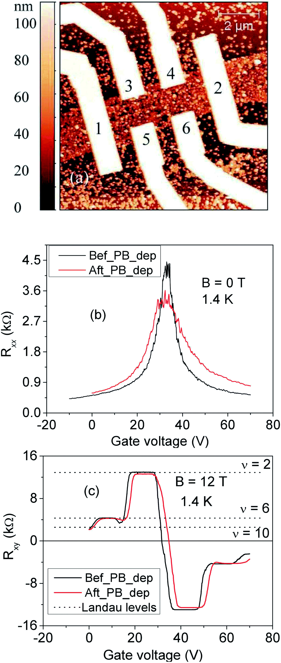 | ||
| Fig. 3 (a) AFM image of a graphene Hall bar after 15 cycles of PB deposition. (b) Longitudinal (Rxx) resistance at zero B-field, and (c) Hall resistance (Rxy) of the graphene sheet before and after 15 cycles of PB deposition. The electrical transport measurements were performed at T = 1.4 K. | ||
Fig. 3(b) and (c) compare the gate-dependent longitudinal (Rxx) and Hall (Rxy) resistance of such a device at T = 1.4 K, which is well below the magnetic ordering temperature of the PB, before and after 15 deposition cycles. No sizeable shift of the resistance maximum in the transfer (Rxx vs. gate voltage) curves can be discerned. This behavior is distinguished from PB-coated individual carbon nanotubes, for which significant p-type doping has been observed.28 One possible explanation for this difference may be the absence of curvature in graphene, which in general leads to a lower chemical reactivity as compared to carbon nanotubes with pronounced curvature of their sidewall. The PB deposition leads to a small decrease in the (field effect) electron (hole) mobility from μ = 5500 (5850) cm2 (V−1 s−1) for pristine graphene to μ = 2500 (4500) cm2 (V−1 s−1) after PB deposition. Such decrease most likely arises from enhanced Coulomb scattering by the ionic centers within the PB. Most remarkably, the deposited PB disturbs only little the quantum Hall effect (QHE) in graphene, as apparent from the still quite sharp Landau plateaus in Fig. 3(c). The robustness of the magnetotransport in the present graphene samples reflects only weak coupling of carriers to the local magnetic moments of the iron centers in the PB. This finding indicates that simple physisorption of a molecular magnet is not sufficient to implement sizeable Rashba SOC or exchange proximity effect into graphene.
In summary, the molecular magnet Prussian blue has been successfully deposited onto graphene flakes using the sequential dip deposition technique. This method yields almost full and uniform PB coverage on graphene for approximately 15 sequential deposition cycles. Strategies to achieve stronger magnetic exchange coupling than in the present graphene/PB hybrids may involve ferromagnetic metal deposition under ultrahigh vacuum conditions or functionalization schemes based upon covalent linkage.
This research was supported by the Landesstiftung Baden-Württemberg in the framework of the Kompetenznetz Funktionelle Nanostrukturen. The authors acknowledge Eva Bruecher for performing the SQUID measurements.
Notes and references
- K. S. Novoselov, V. I. Falko, L. Colombo, P. R. Gellert, M. G. Schwab and K. Kim, Nature, 2012, 490, 192–200 CrossRef CAS PubMed.
- A. K. Geim and K. S. Novoselov, Nat. Mater., 2007, 6, 183–191 CrossRef CAS PubMed.
- N. Tombros, C. Jozsa, M. Popinciuc, H. T. Jonkman and B. J. van Wees, Nature, 2007, 448, 571–574 CrossRef CAS PubMed.
- K. S. Novoselov, A. K. Geim, S. V. Morozov, D. Jiang, Y. Zhang, S. V. Dubonos, I. V. Grigorieva and A. A. Firsov, Science, 2004, 306, 666–669 CrossRef CAS PubMed.
- Y. Zhang, Y.-W. Tan, H. L. Stormer and P. Kim, Nature, 2005, 438, 201–204 CrossRef CAS PubMed.
- A. K. Geim, Rev. Mod. Phys., 2011, 83, 851–862 CrossRef CAS.
- D. R. Dreyer, R. S. Ruoff and C. W. Bielawski, Angew. Chem., Int. Ed., 2010, 49, 9336–9344 CrossRef CAS PubMed.
- Z. Qiao, S. A. Yang, W. Feng, W.-K. Tse, J. Ding, Y. Yao, J. Wang and Q. Niu, Phys. Rev. B: Condens. Matter Mater. Phys., 2010, 82, 161414 CrossRef.
- H. Haugen, D. Huertas-Hernando and A. Brataas, Phys. Rev. B: Condens. Matter Mater. Phys., 2008, 77, 115406 CrossRef.
- Y. G. Semenov, J. M. Zavada and K. W. Kim, Phys. Rev. Lett., 2008, 101, 147206 CrossRef CAS.
- R. Nandkishore and L. Levitov, Phys. Rev. B: Condens. Matter Mater. Phys., 2010, 82, 115124 CrossRef.
- W.-K. Tse, Z. Qiao, Y. Yao, A. H. MacDonald and Q. Niu, Phys. Rev. B: Condens. Matter Mater. Phys., 2011, 83, 155447 CrossRef.
- A. G. Swartz, P. M. Odenthal, Y. Hao, R. S. Ruoff and R. K. Kawakami, ACS Nano, 2012, 6, 10063–10069 CrossRef CAS PubMed.
- A. Kumar, S. M. Yusuf, L. Keller and J. V. Yakhmi, Phys. Rev. Lett., 2008, 101, 207206 CrossRef.
- A. Kumar, S. M. Yusuf and L. Keller, Phys. Rev. B: Condens. Matter Mater. Phys., 2005, 71, 054414 CrossRef.
- S. M. Yusuf, A. Kumar and J. V. Yakhmi, Appl. Phys. Lett., 2009, 95, 182506 CrossRef PubMed.
- H. J. Buser, D. Schwarzenbach, W. Petter and A. Ludi, Inorg. Chem., 1977, 16, 2704–2710 CrossRef CAS.
- F. Herren, P. Fischer, A. Ludi and W. Haelg, Inorg. Chem., 1980, 19, 956–959 CrossRef CAS.
- G. P. Keeley, A. O'Neill, M. Holzinger, S. Cosnier, J. N. Coleman and G. S. Duesberg, Technology, 2013, 01, 58–62 CrossRef.
- Y. Mao, Y. Bao, W. Wang, Z. Li, F. Li and L. Niu, Talanta, 2011, 85, 2106–2112 CrossRef CAS PubMed.
- C. Shan, L. Wang, D. Han, F. Li, Q. Zhang, X. Zhang and L. Niu, Thin Solid Films, 2013, 534, 572–576 CrossRef CAS PubMed.
- L. Cao, Y. Liu, B. Zhang and L. Lu, ACS Appl. Mater. Interfaces, 2010, 2, 2339–2346 CAS.
- D. M. Pajerowski, T. Watanabe, T. Yamamoto and Y. Einaga, Phys. Rev. B: Condens. Matter Mater. Phys., 2011, 83, 153202 CrossRef.
- A. Xidis and V. D. Neff, J. Electrochem. Soc., 1991, 138, 3637–3642 CrossRef CAS PubMed.
- S. Cobo, G. Molnár, F. Carcenac, P. Szilágyi, L. Salmon, C. Vieu and A. Bousseksou, J. Nanosci. Nanotechnol., 2010, 10, 5042–5050 CrossRef CAS PubMed.
- M. D. Mukadam, A. Kumar, S. M. Yusuf, J. V. Yakhmi, R. Tewari and G. K. Dey, J. Appl. Phys., 2008, 103, 123902–123906 CrossRef PubMed.
- A. Kumar, S. M. Yusuf and J. V. Yakhmi, Appl. Phys. A: Mater. Sci. Process., 2010, 99, 79–83 CrossRef CAS PubMed.
- A. Forment-Aliaga, R. T. Weitz, A. S. Sagar, E. J. H. Lee, M. Konuma, M. Burghard and K. Kern, Small, 2008, 4, 1671–1675 CrossRef CAS PubMed.
Footnote |
| † Electronic supplementary information (ESI) available. See DOI: 10.1039/c4ra01079e |
| This journal is © The Royal Society of Chemistry 2014 |