 Open Access Article
 This Open Access Article is licensed under a
 Creative Commons Attribution 3.0 Unported Licence
Coaxial hetero-nanostructures with controllable shell thickness: a “Pore Widening” method†
Pui Yee Loha,
Chenmin Liub,
Chorng Haur Sowc and
Wee Shong Chin*a
aDepartment of Chemistry, Faculty of Science, National University of Singapore, 3 Science Drive 3, Singapore 117543, Singapore. E-mail: chmcws@nus.edu.sg
bNano and Advanced Materials Institute, The Hong Kong Jockey Club Enterprise Center, Hong Kong University of Science and Technology, Clear Water Bay, Kowloon, Hong Kong
cDepartment of Physics, Faculty of Science, National University of Singapore, 2 Science Drive 3, Singapore 117542, Singapore
First published on 17th January 2014
Abstract
This report presents a versatile “Pore Widening” method that can readily lead to arrays of multi-layered one-dimensional (1D) hetero-nanostructures. Using this simple and facile method, we demonstrate that the thickness of the shell component is controllable by the degree of “Pore Widening”. With careful selection of materials and sequences of deposition steps, a variety of polymer–metal, metal–metal and polymer–metal–metal core–shell nanowires, as well as metal oxide nanotubes and metal oxide–metal double-walled nanotubes can be successfully achieved. This opens up a possibility to tailor new properties of 1D hetero-nanostructures through the judicious combination of different core and shell components in the nanometer size regime.
1 Introduction
One-dimensional (1D) core–shell nanowires (NWs) and nanotubes (NTs) have attracted much scientific and technological interest due to their potential applications in solar cells, sensors and energy storage.1–4 Various core–shell hetero-nanostructured architectures have been explored with combinations of different core and shell materials such as semiconductor, metal, metal oxide and conductive polymer.1–20 Some of these nanostructures reported functional advantages, for instance, protection of the core NWs from oxidation,5 fabrication of coaxial p–i–n junction within one strand of core–shell NW,1 etc. Some have also demonstrated enhanced performance due to synergistic effect between the core and shell components.3,4 For a brief review of literatures in this field, a summary is presented in ESI, Table S1.† Various synthetic strategies were used including redox reaction,6 atomic layer deposition (ALD),17 electrospinning15 and high-temperature CVD.1,5,7–9 However, most of these methods involved the use of bulky equipment, high temperature and high vacuum system that increases the cost of fabrication.Another common method to fabricate core–shell 1D hetero-nanostructures is templated synthesis using nanoporous membranes such as anodic aluminium oxide (AAO).10–12,16,18 A range of techniques can be employed with AAO template to generate core–shell hetero-nanostructures such as sol–gel,16 pyrolysis,10 surface thermal oxidation,18 core shrinkage11 and pore etching.12 One of the attractive attributes of templated synthesis is the ability to control the dimensions of the core and shell components independently. However, it is normally more difficult to control the thickness of the shell component. For example, in the “core shrinkage” method,11 the length of the gold sheath in the polyaniline (PANI)–Au core–shell NWs could be controlled but the control of shell thickness remains a challenge. Another work which reported on pore-etching using dilute sodium hydroxide (NaOH) solution also did not show control of the shell thickness.12 Fast dissolution of AAO may make NaOH unsuitable for a good control of pore-etching and the consequent shell thickness. Hence, it would be meaningful to find a general way that can achieve core–shell 1D nanostructures composed of different materials.
In this report, we present a versatile method that can be used to prepare multi-layered 1D hetero-nanostructures with adjustable shell thickness. We have found that slow etching with dilute phosphoric acid (H3PO4) can produce controllable annular gaps surrounding the core NWs or NTs inside the AAO nanochannels (i.e. “pore-widening”). These gaps then allow further deposition of one and even more layers of shell materials onto the core. Through judicious selection of materials and deposition steps, this “Pore Widening” method thus offers possibilities to fabricate various types of bi- and multi-layered core–shell NWs and NTs. We demonstrate the versatility of this approach by fabricating several types of architecture with increasing complexity, i.e. polymer–metal and metal–metal core–shell NWs, metal oxide NTs, polymer–metal–metal multi-layered NWs and metal oxide–metal double-walled NTs (DWNTs).
2 Experimental section
2.1 Synthesis method
The nanostructures described in this paper were grown using electrochemical method. All electrodepositions were carried out using potentiostat/galvanostat Autolab PGSTAT 30. A platinum rod was used as the counter electrode and Ag/AgCl as the reference electrode. Anodic aluminium oxide (AAO) nanopore membranes (Anodisc 47, Whatman Co., pore size ≈ 0.2 μm, thickness ≈ 60 μm, pore density ≈ 109 pores cm−2) were used as templates for deposition. A thin layer of gold sputtered on one side of the AAO prior to electrodeposition served as the working electrode after making contact with the copper foil in a Teflon cell. A hole of about 1 cm in diameter in the Teflon cell defined the area of AAO membrane that was in contact with the electrolytic solution. This formed a three-electrode configuration. After the fabrication steps, the AAO membrane was removed using 1 M NaOH to obtain free-standing array of nanostructures on the thin gold substrate.Each component has its own specific deposition conditions. For electropolymerization of polypyrrole (PPy), the plating solution consists of 0.3 M pyrrole (Acros 99%) and 0.12 M tetraethylammonium tetrafluoroborate (TEABF4, Aldrich 99%) with acetonitrile as the solvent. Deposition was carried out at constant potential [+1.064 V vs. Ag/AgCl (in saturated LiCl/EtOH), charges passed through = 1.0 C]. Deposition of nickel (Ni) component was carried out under a constant current density of −5 mA cm−2 from a typical Watts bath consisting of 165 g L−1 NiSO4·6H2O, 22.5 g L−1 NiCl2·6H2O and 37 g L−1 H3BO3, adjusted to pH 3–4. Copper (Cu) was deposited under a constant current density of −2 mA cm−2 from a copper complex aqueous solution consisting of 80 g L−1 CuSO4·5H2O, 120 g L−1 ethylenediamine and 20 g L−1 KNaC4H4O6·4H2O.
Oxygen reactive ion etching (O2 RIE) was carried out using SAMCO RIE-10N, operated at power of 20 W and pressure of 0.05 Torr. Samples were placed in the chamber and etched for 15 minutes. Heat treatment was carried out in a tube furnace at 400 °C in ambient air for 3 hours.
2.2 Characterization
The morphology of the nanostructures was characterized by Scanning Electron Microscope (SEM) (JEOL JSM 6700-F operating at 5.0 kV and 10 μA). Energy Dispersive X-ray (EDX) analysis for detection of elements was carried out using another SEM instrument equipped with EDX detector (JEOL JSM 6701-F operating at 15.0 kV and 10 μA).3 Results and discussions
Our strategy for the growth of core–shell nanostructures is illustrated in Fig. 1. For demonstration purpose, materials employed are polypyrrole (PPy) as the conductive polymer, and copper (Cu), nickel (Ni) and gold (Au) as the choice of metal components. As shown in Fig. 1, polymer (or first metal M1) was first electrodeposited into the nanochannels of AAO (Step 1). We then immersed the AAO containing the cores into 6 wt% H3PO4 (Step 2). Such solution was found to partially remove the AAO nanochannel walls, leaving an annular gap around the as-prepared cores (“Pore Widening”). Metal (or second metal M2) was subsequently electrodeposited into the gap (Step 3) and 1D core–shell nanostructured arrays could be achieved after removing the template with 1 M NaOH (Step 4).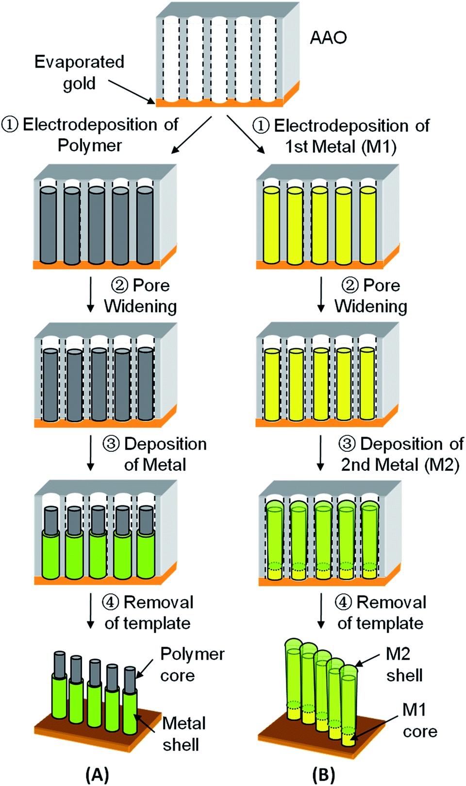 | ||
| Fig. 1 Schematic of the “Pore Widening” steps to generate (A) polymer–metal and (B) metal–metal (M1–M2) core–shell nanostructures. | ||
Since dilute H3PO4 and 1 M NaOH are respectively used for pore-widening and template removal, the choice of materials for the core and inner shell layer is limited to those inert to these two etching solutions. Nonetheless, through judicious selection of materials and sequences of steps, this “Pore Widening” method remain versatile and various desired 1D layered nanostructures can be prepared as demonstrated in the following sub-sections.
3.1 Polymer–metal core–shell nanowires (NWs)
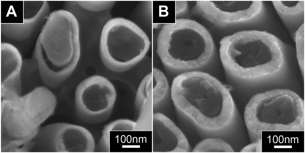
Polymer–metal core–shell NWs such as PPy–Ni can be obtained via the procedure illustrated in Fig. 1A. In this case, there is no limitation to the choice of core polymer as most polymers are inert to 6 wt% H3PO4. In order to prevent the core NWs from being over-grown by the shell, we would grow the core NWs longer than the prospective height of the metal shell to-be grown. To enable preparation of PPy NWs with specific lengths, the electrodeposition was first calibrated as a function of charge deposited as shown in ESI, Fig. S1.† As expected, the length of the PPy NWs can be readily controlled as it increases linearly with respect to the charge deposited.The final PPy–Ni core–shell NWs was characterized using SEM and Fig. 2 shows the side views (A and B) and top views (C and D) SEM images of the core–shell NWs after widening the pores for 1 hour (A and C) and 2 hours (B and D), respectively. The formation of a layer of metal shell around the core polymer after the “Pore Widening” procedure is clearly illustrated. The success of this strategy hinges on the fact that 6 wt% H3PO4 can gently dissolve and polish the walls of the AAO nanochannels, which was the reason for this acid to be widely used in the final step of making AAO membrane.21,22 A closer examination of the SEM images shows that the metal sheath grows thicker with the increase of the pore-widening time. The average shell thickness are estimated to be 25 nm and 55 nm for the pore widening time of 1 hour (Fig. 2A and C) and 2 hours (Fig. 2B and D), respectively. This confirms that the annular gap is created through a slow dissolution of AAO channel walls by the dilute H3PO4. Thus longer immersion duration causes more AAO to dissolve, leading to larger annular gap and thicker shell layer.
 | ||
| Fig. 2 Side (A and B) and top view (C and D) SEM images of the PPy–Ni core–shell NWs prepared after pore widening for 1 hour (A and C) and 2 hours (B and D), respectively. | ||
In order to estimate the shell thickness clearly, the nanostructures were exposed to oxygen reactive ion etching (O2 RIE) for 15 minutes to partially remove the extending PPy NWs. While the samples were exposed to oxygen during this treatment, only slight oxidation was observed by EDX analysis as shown in ESI, Fig. S2.† Hence, we could confirm that the shell thickness is not affected much by this RIE treatment. With the obstructing PPy NWs removed, SEM images in Fig. 3A and B now evidently show the difference in shell thickness corresponding to varying pore-widening time. By systematically varying the duration of pore-widening, a calibration plot of shell thickness as a function of pore-widening time was obtained as shown in ESI, Fig. S3.† The linear calibration plot clearly demonstrates the ability of this method in controlling shell thickness. In addition, this method also enables the deposition of other types of metals readily by using different plating solution (Step 3 in Fig. 1A). We have prepared different PPy–metal core–shell NWs in varying shell thickness, including Au and Cu (see ESI, Fig. S4† for SEM image of PPy–Cu core–shell NWs array prepared).
 | ||
| Fig. 3 Top view SEM images showing different shell thickness of the PPy–Ni core–shell NWs for pore-widening time of (A) 1 hour and (B) 2 hours respectively. Protruding PPy NWs were removed by oxygen reactive ion etching (O2 RIE) treatment. | ||
It is well-known that polymers can be readily removed by suitable solvent dissolution or heat treatment.15,23 Thus, we can envisage using them as “soft template” for the fabrication of NTs with controllable wall thickness prepared through our “Pore Widening” method. This thus opens up another way of making NTs and even multi-layered NTs, in addition to previously reported NTs synthesis.15,16,24,25 Here, we illustrate a one-step process to obtain nickel oxide NTs. Fig. 4A presents the SEM image of the same PPy–Ni NWs as in Fig. 2A after heat treatment at 400 °C for 3 hours in air. Indeed the high temperature burnt away the PPy NWs, leaving behind an array of free-standing NTs. After the heat treatment, it is noted that the shell surface become roughened and the thickness increased from ∼25 nm to ∼60 nm. Both of these observations suggested that the Ni shell have been oxidized to Ni oxide during the heat treatment. This is indeed confirmed by EDX analysis in Fig. 4B, which shows a clear oxygen peak for sample after heat treatment. The roughening of the surface and increased thickness of NTs are due to expansion caused by the intercalation of oxygen into the crystal lattice of Ni metal during heat treatment.
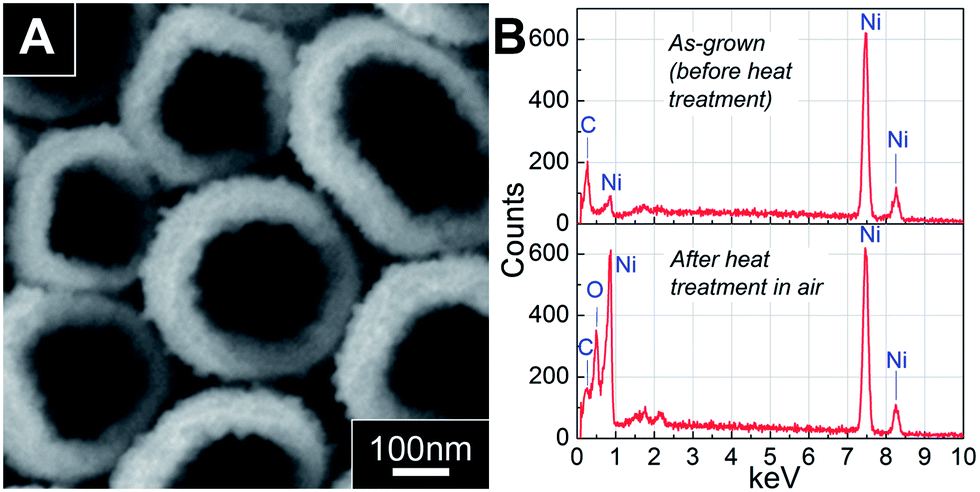 | ||
| Fig. 4 Analysis of PPy–Ni core–shell NWs shown in Fig. 2A after heat treatment at 400 °C in air for 3 hours. (A) Top view SEM image, and (B) a comparison of the EDX spectra before and after heat treatment. | ||
3.2 Metal–metal core–shell nanostructures
This “Pore Widening” approach can be readily applied to fabricate various coaxial multi-layered metal–metal NWs, with the clear limitation that the metal chosen as the core must be inert to the 6 wt% H3PO4 used in the pore-widening step. Synthesis procedure follows the steps illustrated in Fig. 1B for the deposition of M1–M2 core–shell nanostructures. As an example, Cu–Ni core–shell NWs was prepared and the resulting morphology is shown in Fig. 5. The Ni shell and Cu core are clearly distinguishable since the surface of Cu portions often appear roughen due to the formation of a thin layer of oxide when exposed to air. The location of the Ni shell and Cu core is further confirmed via EDX analysis at three different locations: the tip (a), the trunk (b) and the root (c) of the NWs. From the EDX spectra in Fig. 5(a)–(c), it is noted that the relative intensity of Ni to Cu peak gradually decreases from the tips to the roots of the NWs, indicating Ni shells are capping at the tips of the Cu NWs.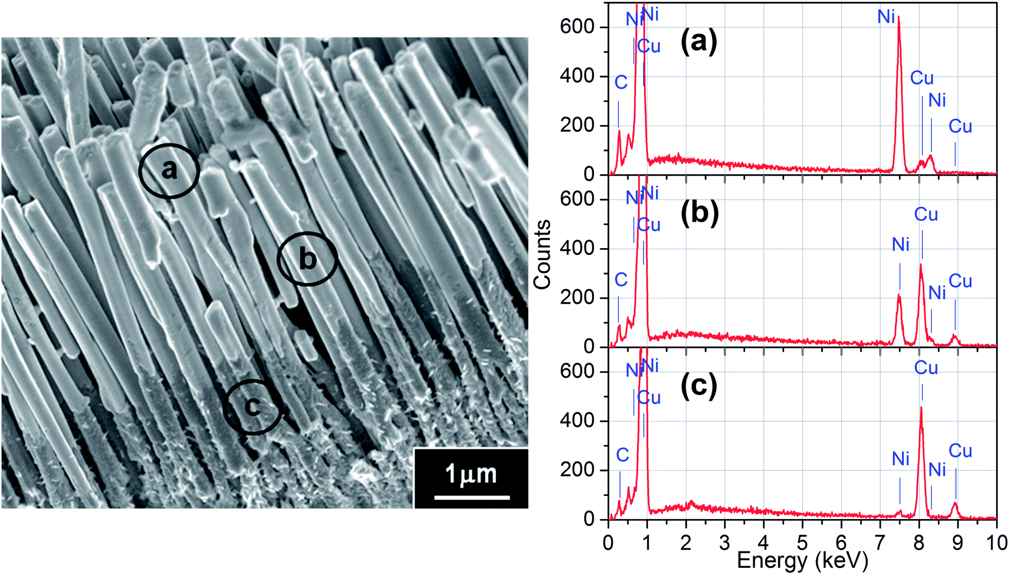 | ||
| Fig. 5 Cu–Ni core–shell NWs array prepared using “Pore Widening” method. The EDX spectra on the right were taken at three different locations marked as (a)–(c) on the SEM image on the left. | ||
A question thus arises: why does the morphology of the prepared metal–metal core–shell NWs (Fig. 5) differ from the polymer–metal core–shell NWs (Fig. 2)? Here, we attempt to rationalize the growth mechanism schematically in Fig. 6. While doped PPy is a conductive polymer, its conductivity is inferior in comparison to metal. Thus, atoms of the shell metal will have higher tendency to deposit directly onto the gold cathode, causing the shell growth to start from the bottom of the widened nanochannels (Fig. 6A). Similar mechanism has been proposed for the preparation of PANI–Au core–shell nanostructure.11 On the other hand, for fabrication of metal–metal (M1–M2) core–shell NWs, the shell deposition can also occur along the length of the conducting core metal (M1) inside the widened gaps as shown in Fig. 6B. Due to “point effect”, the deposition of shell metal (M2) will be more pronounced on the tip rather than at the root of the core metal. The shell layer could thus quickly build up at the tips, blocking further diffusion of metal ions into the bottom gold cathode. This thus prevents the growth of shell at the cathode or at the root of the core metal, resulting in something like the “baseball bat” nanostructure as observed in Fig. 5.
 | ||
| Fig. 6 Schematic sketches of the growth mechanism of (A) polymer–metal and (B) metal–metal core–shell nanostructures in a single channel of AAO template. | ||
3.3 Polymer–metal–metal multi-layered nanostructures
In clear contrast to the “core shrinkage” method,11 deposition is certainly not limited to one single shell component in our proposed method. Additional “Pore Widening” step can be advantageously applied to create space for subsequent deposition of shell materials to give multi-layered NWs. As shown schematically in Fig. 7A, the polymer–metal core–shell NWs obtained after Step 3 in Fig. 1A is subjected to second pore-widening step. An annular gap is produced surrounding the first shell NWs and deposition of the second shell layer can be carried out. An example of such multi-layered core–shell nanostructures is PPy–Cu–Ni tri-layered NWs, with PPy as the core, and Cu and Ni as the first and second shell layer, respectively. The resulting morphology is as shown in the typical SEM image in Fig. 7B. Based on the slight difference in the brightness of the SEM image, we noted again that the outmost shell layer (Ni) is coating only at the tips of the inner shell layer (Cu). This is confirmed by EDX line analysis as shown in ESI, Fig. S5.† The EDX analysis clearly shows that the tips of the shell consist mostly of Ni while larger amount of Cu is exhibited nearer to the root of the NWs. This observation is similar to the deposition of metal–metal core–shell NWs and correlates well to the “point effect” growth mechanism discussed in previous section.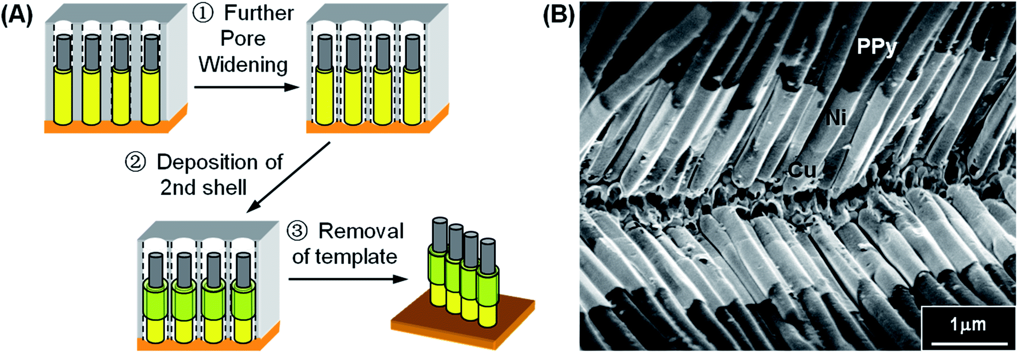 | ||
| Fig. 7 (A) Further “Pore Widening” scheme for the synthesis of polymer–metal–metal tri-layered NWs by repeating steps depicted in Fig. 1. (B) SEM image of PPy–Cu–Ni tri-layered core–shell NWs. | ||
3.4 Metal oxide–metal double-walled nanotubes (DWNT)
We then further demonstrate the versatility of this “Pore Widening” method in generating multi-layered NTs by a sensible selection of materials and sequences of steps. As an example, Fig. 8A shows the utilization of “Pore Widening” method to fabricate metal oxide–metal double-walled NTs (DWNTs). In this case, PPy–Cu core–shell NWs obtained via procedures in Fig. 1A would be the starting material. The core–shell NWs was then subjected to further “Pore Widening” step to produce annular space for the deposition of second layer of shell. Subsequently, the sample was heated to 300 °C for 40 minutes to decompose the PPy core as well as to oxidize the Cu shell to CuxO. This is then followed by the deposition of second shell layer. Removal of the template then resulted in the final CuxO–metal DWNT arrays. Here, Ni was used as the second shell metal and the morphology of the resulting CuxO–Ni DWNTs array is shown in Fig. 8B. Since CuxO is insulating, the subsequent metal shell deposition was found to start from the bottom electrode, thus forming a fairly uniform CuxO–Ni DWNTs.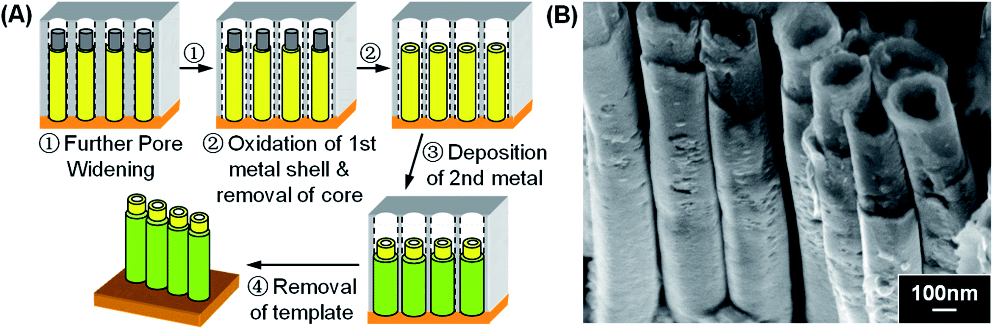 | ||
| Fig. 8 (A) Schematic procedures for the synthesis of metal oxide–metal double-walled NTs. (B) SEM image showing CuxO–Ni double-walled NTs. | ||
To confirm the elemental profile of this DWNTs, EDX line analysis was carried out and the spectrum obtained is presented in ESI, Fig. S6.† The cartoon at the bottom of the figure gives an illustration for better understanding of the EDX spectrum. Based on this analysis, the tips of the DWNTs consist of mainly Cu with certain amount of O, indicating the presence of CuxO that was supposed to be the inner wall. These signals from the inner wall are detected since the inner wall is not over-grown by the outer shell and is seen protruding from the DWNTs in the SEM images in both Fig. 8B and ESI, S6.† Meanwhile, the outmost layer from the root of the NTs shows signal of Ni, confirming the part grown as the outer shell consists of Ni. This demonstrates the successful deposition of CuxO–Ni DWNT via the “Pore Widening” method.
4 Conclusions
In summary, we have demonstrated the versatility of “Pore Widening” method in creating various coaxial multi-layered 1D hetero-nanostructures. Dilute H3PO4, which has been used to chemically remove the barrier layer during the fabrication of AAO membrane, is advantageously used here to slowly etch away an annular gap between the deposited core and the wall of AAO nanochannel. The presence of this gap allows the deposition of another layer of material as the sheath, forming coaxial 1D hetero-nanostructure. Besides, it was shown that the size of the annular gap, and thus the subsequent thickness of the shell, can be controlled by carefully tuning the duration of pore widening. This is of course limited by the thickness of the AAO nanochannel walls.Expanding from the architectures demonstrated here, we suggest that our “Pore Widening” method can be used to fabricate coaxially multi-layered NWs and NTs with varied combinations of materials. As in most AAO templated synthesis, the final core and shell components must be inert to NaOH used to remove the template. Thus, in addition to Au, Cu, Ni and PPy demonstrated in this report, other possible materials include PANI,11 poly(p-phenylene vinylene),26,27 silver,28 SiO2,16 ZnS,19 Bi and Bi2O3.18 The additional limitation of “Pore Widening” method, of course, is that the core or inner shell material must also be inert to dilute H3PO4. We believe many polymeric materials are suitable in this aspect, as well as most of the inert metals and elements. Hence, we envisage that many interesting nanostructures can be generated using this “Pore Widening” approach which will be useful in potential functional devices in various areas.
Acknowledgements
This research work is supported by the National University of Singapore Academic Research Fund R-398-000-010-112.Notes and references
- B. Z. Tian, X. L. Zheng, T. J. Kempa, Y. Fang, N. F. Yu, G. H. Yu, J. L. Huang and C. M. Lieber, Nature, 2007, 449, 885–890 CrossRef CAS PubMed.
- X. H. Xia, J. S. Luo, Z. Y. Zeng, C. Guan, Y. Q. Zhang, J. P. Tu, H. Zhang and H. J. Fan, Sci. Rep., 2012, 2, 981 Search PubMed.
- C. Y. Yan, H. Jiang, T. Zhao, C. Z. Li, J. Ma and P. S. Lee, J. Mater. Chem., 2011, 21, 10482–10488 RSC.
- X. H. Xia, J. P. Tu, Y. Q. Zhang, X. L. Wang, C. D. Gu, X. B. Zhao and H. J. Fan, ACS Nano, 2012, 6, 5531–5538 CrossRef CAS PubMed.
- Y. C. Zhu, Y. Bando, D. F. Xue, F. F. Xu and D. Golberg, J. Am. Chem. Soc., 2003, 125, 14226–14227 CrossRef CAS PubMed.
- X. G. Wen and S. H. Yang, Nano Lett., 2002, 2, 451–454 CrossRef CAS.
- Q. Li and C. R. Wang, Appl. Phys. Lett., 2003, 82, 1398–1400 CrossRef CAS PubMed.
- Y. B. Li, Y. Bando, D. Golberg and Z. W. Liu, Appl. Phys. Lett., 2003, 83, 999–1001 CrossRef CAS PubMed.
- S. Y. Bae, H. W. Seo, H. C. Choi, D. S. Han and J. Park, J. Phys. Chem. B, 2005, 109, 8496–8502 CrossRef CAS PubMed.
- J. C. Bao, K. Y. Wang, Z. Xu, H. Zhang and Z. H. Lu, Chem. Commun., 2003, 208–209 RSC.
- M. Lahav, E. A. Weiss, Q. B. Xu and G. M. Whitesides, Nano Lett., 2006, 6, 2166–2171 CrossRef CAS PubMed.
- W. R. Hendren, A. Murphy, P. Evans, D. O'Connor, G. A. Wurtz, A. V. Zayats, R. Atkinson and R. J. Pollard, J. Phys.-Condes. Matter, 2008, 20, 362203 CrossRef.
- H. Wang, C. W. Xu, F. L. Cheng, M. Zhang, S. Y. Wang and S. P. Jiang, Electrochem. Commun., 2008, 10, 1575–1578 CrossRef CAS PubMed.
- I. T. Jeon, M. K. Cho, J. W. Cho, B. H. An, J. H. Wu, R. Kringel, D. S. Choi and Y. K. Kim, J. Mater. Chem., 2011, 21, 12089–12095 RSC.
- D. Li and Y. N. Xia, Nano Lett., 2004, 4, 933–938 CrossRef CAS.
- N. I. Kovtyukhova, T. E. Mallouk and T. S. Mayer, Adv. Mater., 2003, 15, 780–785 CrossRef CAS.
- J. Hwang, B. D. Min, J. S. Lee, K. Keem, K. Cho, M. Y. Sung, M. S. Lee and S. Kim, Adv. Mater., 2004, 16, 422–425 CrossRef CAS.
- L. Li, Y. W. Yang, G. H. Li and L. D. Zhang, Small, 2006, 2, 548–553 CrossRef CAS PubMed.
- D. Z. Zhang, L. A. Luo, Q. Liao, H. Wang, H. B. Fu and J. N. Yao, J. Phys. Chem. C, 2011, 115, 2360–2365 CAS.
- J. D. Fan, C. Fabrega, R. Zamani, A. Shavel, F. Guell, A. Carrete, T. Andreu, A. M. Lopez, J. R. Morante, J. Arbiol and A. Cabot, J. Alloys Compd., 2013, 555, 213–218 CrossRef CAS PubMed.
- G. E. Thompson and G. C. Wood, Nature, 1981, 290, 230–232 CrossRef CAS.
- H. Masuda and K. Fukuda, Science, 1995, 268, 1466–1468 CAS.
- Polymer data handbook, ed. J. E. Mark, Oxford University Press, New York, 2nd edn, 2009 Search PubMed.
- L. Li, Y. W. Yang, X. H. Huang, G. H. Li, R. Ang and L. D. Zhang, Appl. Phys. Lett., 2006, 88, 103119 CrossRef PubMed.
- X. C. Dou, G. H. Li, X. H. Huang and L. Li, J. Phys. Chem. C, 2008, 112, 8167–8171 CAS.
- F. Massuyeau, J. L. Duvail, H. Athalin, J. M. Lorcy, S. Lefrant, J. Wery and E. Faulques, Nanotechnology, 2009, 20, 155701 CrossRef CAS PubMed.
- P. Y. Loh, C. M. Liu, C. H. Sow and W. S. Chin, manuscript in progress.
- L. D. Qin, S. Park, L. Huang and C. A. Mirkin, Science, 2005, 309, 113–115 CrossRef CAS PubMed.
Footnote |
| † Electronic supplementary information (ESI) available: Table summarising reported synthesis of core–shell NWs and NTs in the literature, SEM image of PPy NWs and calibration plot of NWs length, EDX analyses of PPy–Ni core–shell NWs before and after O2 RIE, plot of Ni shell thickness vs. pore-widening time, SEM image of PPy–Cu core–shell NWs, and EDX line analyses of PPy–Cu–Ni tri-layered core–shell NWs and CuxO–Ni DWNT. See DOI: 10.1039/c4ra00045e |
| This journal is © The Royal Society of Chemistry 2014 |