DOI:
10.1039/C3RA48046A
(Paper)
RSC Adv., 2014,
4, 13774-13781
Simulation of the electrohydrodynamic instability process used in the fabrication of hierarchic and hollow micro/nanostructures
Received
30th December 2013
, Accepted 5th March 2014
First published on 7th March 2014
Abstract
This article demonstrates that the electrohydrodynamic patterning process, a novel technique for the manufacturing of micro- and nano-scale structures, also allows the one-step realization of hierarchical structures and hollow structures. Through numerical simulation, it is shown that multilevel structures can be obtained if process time and applied electric voltage are optimized. As an example, the growth of structures with a width of around 187 nm and depth of 95 nm has been successfully simulated alongside structures with width of around 0.4 μm and depth of 0.8 μm. The width of the protrusive mask patterns is shown to determine whether hollow structures with single or multiple shapes can be formed using electric field assisted capillarity. The numerical simulation process effectively demonstrates that the realization of micro/nano-structures with hierarchic and multilevel shapes can be considered as an innovative manufacturing process for MEMS or micro/nanofluidic structures.
Introduction
Electrohydrodynamic instability patterning is a novel technique, which has potential applications for the economical and efficient manufacturing of micro- and nano-scale structures.1–3 This technology takes advantage of the Maxwell stress generated by two media of different dielectric constants subjected to an electric field, to induce the self-assembling micro/nanostructures in one of the media. A number of studies on the electric induced destabilization mechanisms have been investigated for their usefulness in lithography.4–19 The spontaneous formation of periodical pillars with space equaling the most unstable wavelength induced by the electric field has been well characterised as well as its capability to generate three-dimensional structures even without the requirement of a patterned mask.8 The heterogeneous electric field generated by a patterned mask should be used however to realize precise control over the emerging pattern in the film. The patterned template induces a laterally varying electric field that has a two-fold influence on the development of the surface instability. Firstly, the instability is directed towards the template protrusions due to the pressure gradients induced by the height variations of the template. In addition, these protrusions generate a larger electric field strength that leads to a locally increased growth rate of the instability. As a consequence, a positive replica of the template structure is obtained. The generation of a modulated electric field can be implemented either by a patterned conducting surface,20–24 dielectric patterns on a conductive substrate25 or electrically conductive patterns on a dielectric substrate.26
More recently, a method combining electrostatic field and capillarity effects was demonstrated to form hollow structures.27,28 The resulting Electrical Field Assisted Capillarity (EFAC) process, as an extension of the Electrohydrodynamic Induced Patterning (EHDIP) method, is a novel manufacture process of hollow microstructures. The notable difference of EFAC from EHDIP is that the top electrode is a heavily wetted, low surface energy surface, which subjects the polymer to a large capillary force when it reaches the surface of the top mask, thus enabling the rapid coating of the mask and the formation of a shell of a few microns thick. In this paper, we demonstrate that hierarchic or multilevel hollow structures can be obtained in one step by using a conductive patterning template on a dielectric substrate via electric field assisted capillarity.
In the past, a non-linear 3D model proposed by Verma et al.29 to simulate the EHDIP process revealed that patterns formed by a heterogeneous electric field were determined by the interplay of two lateral length scales that are intrinsic to this process. One length scale is the destabilization wavelength, which is determined by the balance of the destabilizing electrostatic pressure gradient and the restoring interfacial tension. The other length scale is the periodicity of the patterned master template. Therefore, it is necessary to study how to utilize the structured electric field to suppress the intrinsic characteristic wavelength corresponding to the first length scale mentioned before by optimizing the process parameters. Our previous work was devoted to answer the above-mentioned question.30 For many applications, however, it is desirable to control the spatial arrangement of more than one component. With traditional methods, this requires an iterative, multistep procedure, making the replication process more complex and less reliable. Electrohydrodynamic instability can produce a hierarchical lateral structure that exhibits two independent characteristic dimensions.31–36
In this article, we aim to extend the application of EHDIP and EFAC in realizing micro/nano-structures with hierarchic and variable multilevel shapes. To further understand the fundamentals of EHDIP and EFAC process, theoretical models based on the finite element analysis simulation software COMSOL Multiphysics (version 4.3) have been developed in this paper. It is demonstrated that hierarchical structures and hollow structures can be realized in one step. For EHDIP, the influence of operational parameters such as the width and height of master electrode, electrodes spacing, the period of master electrode and initial film thickness has been studied in detail to realize the formation of hierarchical structures.
Presentation of the simulation model
Consider a viscous polymer film surrounded by air and resting on a planar substrate under the influence of a heterogeneous electric field, as shown in Fig. 1. Fig. 1(a) shows a conductive patterned electrode and planar substrate. Fig. 1(b) shows the conductive patterns on a dielectric substrate. For a patterned mask, the height of the electrode protrusions, the width of the electrode protrusions, and the period of the grating mask are denoted by p, w and l, respectively. The master electrode applied with voltage u is positioned above the substrate at distance d. The points A, B, and C in Fig. 1(a) are specified positions used to demonstrate the pressure jump in the film.
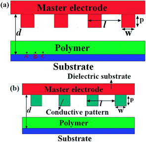 |
| | Fig. 1 Schematic diagrams of a polymer film resting on a planar substrate under the influence of a heterogeneous electric field. (a) presents the mask as a conductive patterned electrode. (b) shows the mask as a type of conductive pattern on a dielectric substrate. | |
Numerical method
In this work, the level set two-phase flow application and electrostatic modules in COMSOL Multiphysics are adopted to simulate EHDIP.30,37,38 The conservative level set method is an interface tracking method, which is used for computing multiphase flow problems. The interface between fluid (gas and liquid) is represented by the 0.5 contour value of the level set function ϕ whose range is between 0 and 1. A smeared out Heavisides function considers that ϕ < 0.5 for one phase, ϕ > 0.5 for the other and the transition is varied smoothly across the interface. The level set equation is expressed as:| |
 | (1) |
where γ is the stabilization parameter; ε is the parameter that controls the interface thickness and should have the same order as the computational mesh size of the elements where the interface propagates; U is the velocity vector of the interface, which can be solved by the Navier–Stokes (N–S) equations. The momentum equation,| |
 | (2) |
and the continuity equation,| |
 | (3) |
are the N–S equations, where ρ is the density, μ is the viscosity and p is pressure. F is the volume force caused by the atmospheric pressure p0, the surface tension Fst = σκδn, and the electrostatic pressure pel. F = (p0 + σκ + pel)δn, where σ is the surface tension coefficient (N m−1), κ is the curvature, δ is a delta function concentrated to the surface, and n is the unit outward normal to the interface. δ smoothens the surface tension which is concentrated at the interface between fluids and is approximated according to the equation
The interface normal vector modulus and the interface curvature are determined by eqn (5) and (6) respectively.
| |
 | (5) |
| |
 | (6) |
The density and viscosity are calculated from
where
ρ1 and
ρ2 are the fluid densities of the air and polymer film;
μ1 and
μ2 indicate the dynamic viscosities of the air and the polymer film. The electric field is solved using the Laplace's equation for the voltage assuming that there is zero free charge in the bulk fluid:
The electrostatic pressure can be described by the following equation:17
| | |
pel = −0.5ε0εp(εp − 1)Ep2
| (10) |
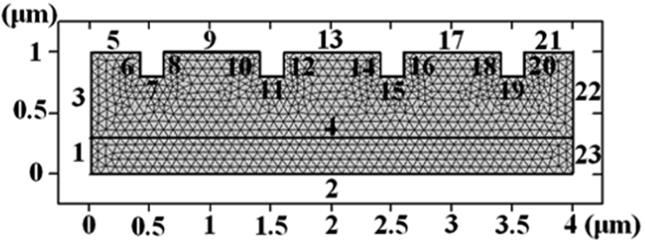
For convenience, the schematic diagrams of the EHDI process on planar substrate (Fig. 1(a) and (b)) are taken to show the geometry, boundary conditions and mesh of the two-dimension model. In order to highlight versatility and exhibit the process evolution, only four periods of the pattern on master electrode are shown here. The geometry and mesh of the model are presented in Fig. 2. For a conductive patterned electrode, a DC voltage is applied between the bottom (boundary 2) and the top electrode with electrical potential (boundaries 5, 6, 7, ⋯, 19, 20 and 21). For a partial conductive electrode, i.e. conductive pattern on a dielectric substrate, the boundary 5, 9, 13, 17 and 21 are set to be at zero potential; the other boundary conditions are similar to those of the conductive patterned electrode. The boundary conditions for the fluid flow are: (a) no slip at boundaries 2, 5, 6, 7, ⋯, 19, 20 and 21; (b) periodic boundary on boundaries 1, 3, 22 and 23; (c) initial fluid interface at boundary 4. In order to simulate a periodic structure, it is necessary to introduce the periodic boundary conditions at boundaries 1, 3, 22 and 23. The sources 1 and 3 corresponding to the destinations 23 and 22, respectively. The expressions for the sources are the pressure in the fluid P and the flow velocity U. Two-phase flow is in the form of conservative level set. Properties of the polymer liquid used in the simulation are presented in Table 1.
 |
| | Fig. 2 Schematic diagram introducing the geometry, boundary conditions and mesh of the two-dimension model. Dimension unit is μm. | |
Table 1 Properties of the material used in the numerical simulations
| Simulated dynamic viscosity (Pa s) |
Density (kg m−3) |
Dielectric constant |
Surface tension (N m−1) |
| 1 |
1000 |
2.5 |
0.038 |
Results and discussions
The periodic pattern on the template generates a periodic electric field on the air–polymer interface, where the larger electric field intensity corresponds to the protrusion on the template, and the lower electric field intensity corresponds to the cavity. So the electrostatic force on the polymer–air interface is periodic considering that the electrostatic force is an almost square relation to the electric filed strength. This modulated electrostatic force attracts the polymer as it moves upwards to form structures similar to the patterns on the template.
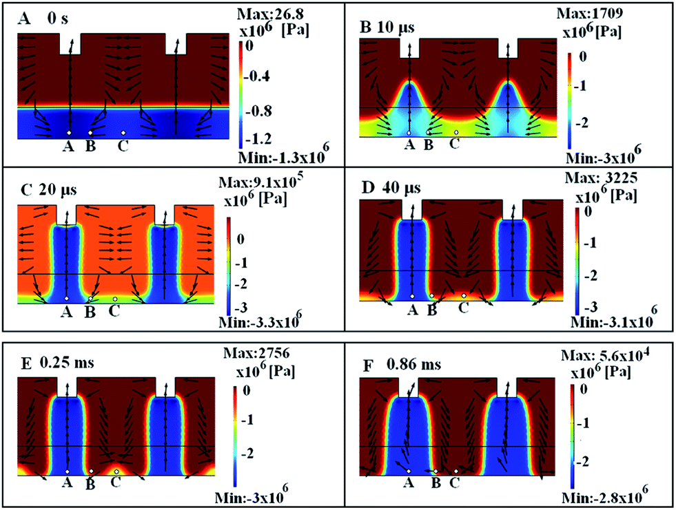
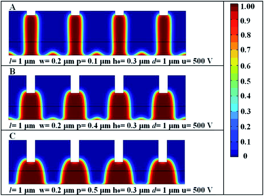
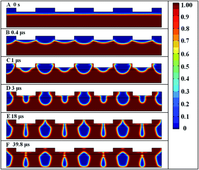
The detailed time evolution of the electrically induced patterning process with patterned conductive template is shown in Fig. 3. Simulation results show a two-dimensional periodic microstructure induced by a conductive patterned electrode with protrusion height of 0.2 μm and width of 0.2 μm. The period l of the protrusion is 1 μm. The gap d between the electrodes is 1 μm. The initial polymeric film thickness is 0.3 μm. The applied DC voltage on the top electrode is 500 V and the bottom electrode is grounded. Initially the polymer film surface is flat as shown in Fig. 3(A). As the spatial heterogeneity of the electrostatic field is introduced by the patterned top electrode, the polymer liquid grows upwards firstly under the protrusions of the top electrode due to the higher electric field in those areas as shown in Fig. 3(B). The resulting uplifted polymer experiences a greater electrostatic force as the polymer approaches the top electrode, pulling the polymer fluid further towards the protrusion of the top electrode. The growing polymer touches the surface of the top electrode, and is stopped from moving further upwards as indicated in Fig. 3(C). Since the larger electrostatic force difference emerges at the boundaries of the polymer columns, the polymer material at the boundaries is rapidly depleted, leaving residual polymer between the columns as shown in Fig. 3(D). As the process is developing, the residual polymer forms small humps, hence the multilevel structures can be obtained in one step as shown in Fig. 3(E). However these humps do disappear for a suitably long duration of the process such that the complete replica of the mold can be obtained with potentially a larger height-to-width aspect ratio. It is found that if the applied voltage is less than 500 V, the intermediate evolution stages, shown in Fig. 3(D) and (E), do not appear. In this case, the hierarchical structures cannot be obtained. In this particular case, large structures with width of around 187 nm (full-width at half-maximum) and depth of 95 nm can be created concomitantly with structures of 400 nm width and 800 nm depth as shown in Fig. 3(E). In general, similar multilevel structures can be obtained for large applied voltage values and moderately short process times.
 |
| | Fig. 3 Spatiotemporal evolution of a 0.3 μm thick polymer liquid interface. Red color represents the polymer liquid, and the blue represents air. | |
The mechanism behind the flow phenomenon shown in Fig. 3 is the uneven pressure distribution in the film. Fig. 4 shows how the pressure distribution and velocity values change during the process. The spatial heterogeneity of the electrostatic field induces the uneven pressure distribution on the film surface. The pressure difference between point A and C is about 7.6 105 Pa induces the transverse flow. The pressure difference becomes larger during the columns formation and is about 8.74 105 Pa between points A and C as shown in Fig. 4(B). In the Fig. 4(B), the pressure difference between point A and B reaches to 1.24 106 Pa, but the pressure difference between points B and C is just 0.31 106 Pa, therefore the larger pressure gradient between A and B leads to more fluid flowing to the corner area. As a result, the polymer material at point B is depleted as shown in Fig. 4(D). Finally, hierarchical structures form in the polymeric film as shown in Fig. 4(E).
 |
| | Fig. 4 Variations of the pressure (color) and velocity (black arrows) at various time steps for the case of Fig. 3. | |
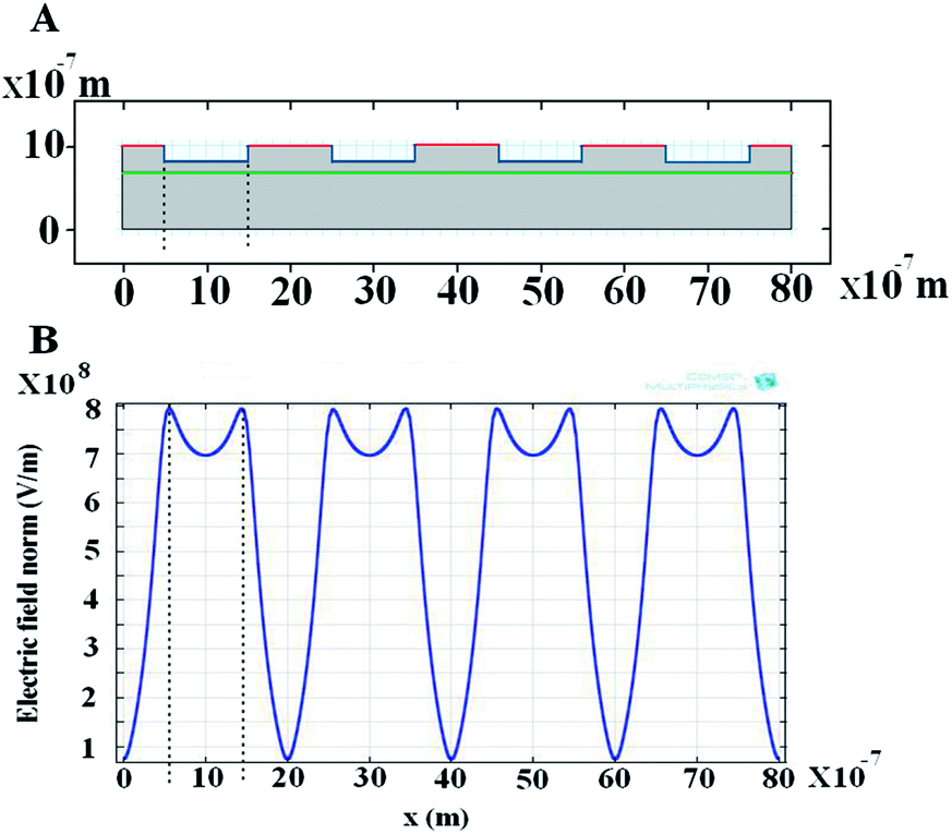
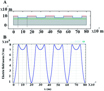
Fig. 5 shows the diagram of polymer film and the electric field strength distribution at the film surface at the initial stage. The electric field distribution follows a sinusoidal profile. The electric field strength underneath the center of the protrusion is much larger than in the other areas, such that a larger electrostatic force is exerted on the film surface. Accordingly, the internal pressure at this point is higher than in the other areas.
 |
| | Fig. 5 Electrically induced hierarchical structures for a patterned template. (A) Diagram of polymer film at initial time, the red line is the shape of the protrusions of the master electrode and the green line is the air–polymer interface. (B) Initial electric field strength located at the surface of the polymer film. The dotted line is used to characterize the largest electric field strength located at the surface of the polymer film. | |
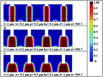
Furthermore, we have studied in detail how the change of process parameters, such as electrode geometries (d, l, w, p) as well as polymer layer thickness affect the formation of the hierarchical structures based on the results in Fig. 3. Fig. 6 shows the changing trend of the hierarchical structures under different widths of electrode protrusions w. It can be clearly seen that the hierarchical structures can be obtained without considering the change of the width of electrode protrusions. However, the change of the width of the electrode protrusions influences the heights of small humps, the maximum height of the hump is obtained for the width of the electrode protrusions reaching 0.5 μm, meaning filling factor (w/l) is 0.5. In general, the change of the width of the electrode protrusion w does not affect largely the formation of the hierarchical structures.
 |
| | Fig. 6 The final hierarchical structures induced by electric field with the different width of the electrode protrusions w. Red color represents the viscous polymer, and blue represents air. | |
Fig. 7 shows the variation of hierarchical structures against the electrode spacing d. The hierarchical structures can be obtained with the smaller electrode spacing d in Fig. 7(A), with the increase of the electrode spacing, the height of the small humps decreases as shown in Fig. 7(B), in extreme cases, no small humps are presented as in Fig. 7(C). In general, the increase of the electrode spacing d was unfavourable for the formation of the hierarchical structures.
 |
| | Fig. 7 The changing trend of hierarchical structures induced by electric field with the different electrode spacing d. Red color represents the viscous polymer, and blue represents air. | |
Fig. 8 shows how the changes of the film thickness affect the formation of the hierarchical structures. The largest height of the small humps can be obtained when the film thickness is minimal as shown in Fig. 8(A); no hierarchical structures were present when the film thickness is larger as in Fig. 8(C). In general, the increase of the film thickness will largely go against for the formation of the hierarchical structures.
 |
| | Fig. 8 The changing trend of hierarchical structures induced by electric field with the different film thickness. Red color represents the viscous polymer, and blue represents air. | |
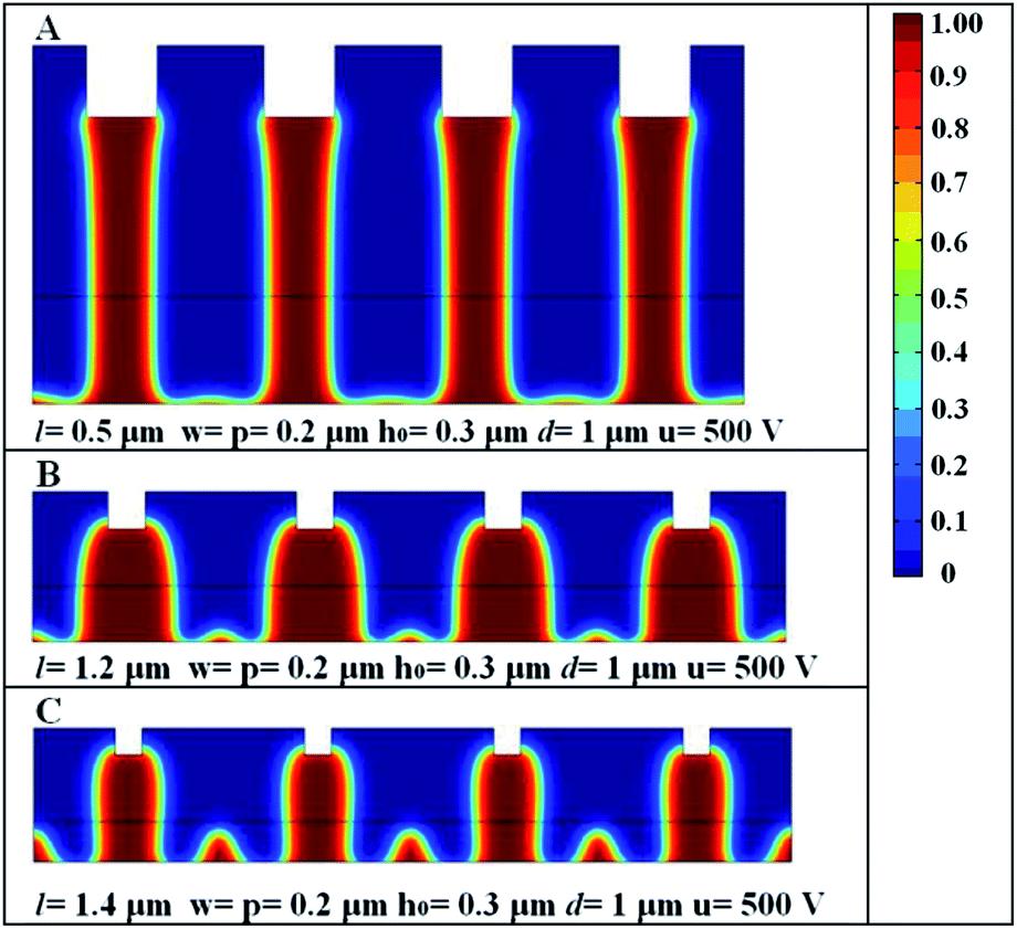
Fig. 9 shows how the changes of the distance of the electrode protrusions (i.e. the period l) influence the formation of the hierarchical structures. The largest height of the small humps can be obtained when the distance of the electrode protrusions is maximum as shown in Fig. 9(C); no hierarchical structures were present when the distance of the electrode protrusions is small as in Fig. 9(A). In general, the increase of the distance of the electrode protrusions will certainly help the formation of the hierarchical structures.
 |
| | Fig. 9 The final hierarchical structures induced by electric field with the different distance of the electrode protrusions (l–w). Red color represents the viscous polymer, and blue represents air. | |
Fig. 10 shows how the changes of the different height of the electrode protrusions influence the formation of the hierarchical structures. The largest height of the small humps can be obtained when the height of the electrode protrusions is minimum as shown in Fig. 10(A); the independent structure of columns underneath the protrusions appears with no formation of the small humps as in Fig. 10(C). In general, the decrease of the height of the electrode protrusions is beneficial to the formation of the hierarchical structures.
 |
| | Fig. 10 The final hierarchical structures induced by electric field with the different height of the electrode protrusions. Red color represents the viscous polymer, and blue represents air. | |
Fig. 11 shows the simulation results of multilevel periodic hollow microstructures induced by the conductive pattern on a dielectric substrate via electric field assisted capillarity. Here the electrode protrusion is 0.2 μm high and 1 μm wide. The gap d between the protrusions is 1 μm, the period l is 2 μm, and the initial film thickness is 0.68 μm with a 0.12 μm gap between the film surface and lowest part of the electrode. The applied DC voltage is 420 V.
 |
| | Fig. 11 Spatiotemporal evolution of multiple hollow structures for 0.68 μm initial film thickness. Red color represents the polymer liquid, and the blue represents air. | |
The process starts in the same way with a thin polymer film between two electrodes as shown in Fig. 11(A). Due to the high contrast of the electrostatic force at the corner of the electrode protrusions and as long as the width of the protrusion is relatively large, the periodic concave structures emerge at the surface of the polymer as presented in Fig. 11(B). The process differs from EHDIP when the polymer reaches the top mask as shown in Fig. 11(C). Since the top mask is hydrophilic, the capillary force will drive the polymeric liquid flow along the surface of the top electrode as indicated in Fig. 11(D). As a result, the flow of the fluid will meet at the middle point of the protrusions as well as the middle point of the gap between protrusions as shown in Fig. 11(E). Finally, the multilevel hollow structures can be formed in the polymeric film, Fig. 11(F). The diameter of the small hollow structures is 36 nm. However, if the aspect ratio of height to width of the electrode protrusions is increased, only hollow structures under the cavity can be obtained.28 As a result, the width of the protruding mask pattern is critical to determine if single or multiple hollow structures can be formed by the EFAC process.
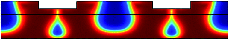
Fig. 12 shows how the pressure distribution and velocity changes during the hollow structures evolution corresponding to Fig. 11. Initially there is a pressure jump of around 7.51 105 Pa in the film underneath the corners of the protrusion. The jump is caused by the heterogeneous electric field shown in Fig. 13. In the whole process, the pressure inside the hollow structures is larger than that in the surrounding polymeric fluid and the pressure jump is maximal at the bottom of the hollow structures, so the hollow structures moves down.
 |
| | Fig. 12 Evolution of the pressure (color) and velocity (black arrows) at various time steps for the case shown in Fig. 11. The pressure unit is Pa and the velocity unit is m s−1. | |
 |
| | Fig. 13 Electrically induced hollow structures for a patterned template. (A) Diagram of polymer film at initial time, the red line together with the blue line is the shape of the protrusions of the master electrode with electrically conductive patterns (the blue line) on a dielectric substrate (the red line) and the green line is the air–polymer interface. (B) Initial electric field distribution on the film surface for the case of hollow structures shown in Fig. 11. The dotted line is used to characterize the largest electric field strength located at the surface of the polymer film. | |
In the process of forming hollow structures, the diagram of polymer film and the electric field strength distribution on the film surface at the initial stage is showed in Fig. 13. The much larger strength of electric field underneath the corners of the protrusions leads to the larger gradient of the electrostatic force at the corners, which induces unstability of the film at these points first.
Fig. 14 shows the simulation results of both sealed hollow microstructures and non-sealed open microstructures induced by the conductive pattern on a dielectric substrate via electric field assisted capillarity. Here the electrode protrusion is 0.2 μm high and 1 μm wide. The gap d between the protrusions is 1 μm, the period l is 3 μm, and the initial film thickness is 0.65 μm with a 0.15 μm gap between the film surface and lowest part of the electrode. The applied DC voltage is 420 V.
 |
| | Fig. 14 The simulation results shows that both sealed hollow microstructures and non-sealed open microstructures can co-exist. Red color represents the polymer liquid, and the blue represents air. | |
Conclusions
In summary, we have demonstrated through simulations that multilevel structures can be obtained by the proper control of EHDIP process parameters. It is found that smaller initial film thickness, smaller electrode spacing and larger distance of the electrode protrusions help to achieve the hierarchical structures. Furthermore, it is found that a proper width of the electrode protrusion and smaller height of the electrode protrusion are helpful to achieve hierarchical structures. Moreover, it is found that the electric field assisted capillarity can create hierarchic hollow structures using a patterned master electrode. Numerical computing results show that hollow structures with diameter of 36 nm can be achieved. The structures with both sealed hollow structures and non-sealed open structures co-existing can be obtained. Our results shed some light on the mechanisms by which multiple patterns in the form of hierarchical structures or hollow structures can be formed in the film. These unique structures have potential applications in MEMS or micro/nanofluidics.
Acknowledgements
The authors acknowledge the financial support from Natural Science Foundation of China under grant numbers 90923036 and 60977041 as well as the Ministry of Sciences and Technology of China under grant number 2010DFR10660. The financial support of the UK Innovative electronic Manufacturing Research Centre (IeMRC) is also acknowledged through the funding of the Flagship project “Smart Microsystems” (FS/01/02/10).
Notes and references
- S. Y. Chou, L. Zhuang and L. Guo, Appl. Phys. Lett., 1999, 75, 1004–1006 CrossRef CAS.
- S. Y. Chou and L. Zhuang, J. Vac. Sci. Technol., B: Microelectron. Nanometer Struct.–Process., Meas., Phenom., 1999, 17, 3197–3202 CrossRef CAS.
- P. Deshpande, X. Sun and S. Y. Chou, Appl. Phys. Lett., 2001, 79, 1688–1690 CrossRef CAS.
- E. Schäffer, T. Thurn-Albrecht, T. P. Russell and U. Steiner, Europhys. Lett., 2001, 53, 518–524 CrossRef.
- L. F. Pease III and W. B. Russel, J. Non-Newtonian Fluid Mech., 2002, 102, 233–250 CrossRef.
- V. Shankar and A. Sharma, J. Colloid Interface Sci., 2004, 274, 294–308 CrossRef CAS PubMed.
- N. Arun, A. Sharma, P. S. G. Pattader, I. Banerjee, H. M. Dixit and K. S. Narayan, Phys. Rev. Lett., 2009, 102, 254502 CrossRef CAS PubMed.
- Z. Lin, T. Kerle, S. M. Baker, D. A. Hoagland, E. Schäffer, U. Steiner and T. P. Russell, J. Chem. Phys., 2001, 114, 2377–2381 CrossRef CAS.
- K. Amanda Leach, Z. Lin and T. P. Russell, Macromolecules, 2005, 38, 4868–4873 CrossRef.
- Z. Lin, T. Kerle, T. P. Russell, E. Schäffer and U. Steiner, Macromolecules, 2002, 35, 3971–3976 CrossRef CAS.
- J. Bae, E. Glogowski, S. Gupta, W. Chen, T. Emrick and T. P. Russel, Macromolecules, 2008, 41, 2722–2726 CrossRef CAS.
- S. Herminghaus, Phys. Rev. Lett., 1999, 83, 2359–2361 CrossRef CAS.
- G. Narsimhan, J. Colloid Interface Sci., 2005, 287, 624–633 CrossRef CAS PubMed.
- H. Xiang, Y. Lin and T. P. Russell, Macromolecules, 2004, 37, 5358–5363 CrossRef CAS.
- N. Arun, A. Sharma, V. B. Shenoy and K. S. Narayan, Adv. Mater., 2006, 18, 660–663 CrossRef CAS.
- D. Tseluiko, M. G. Blyth, D. T. Papageorgiou and J.-M. Vanden-Broeck, J. Fluid Mech., 2008, 597, 449–475 Search PubMed.
- K. John, P. Hanggi and U. Thiele, Soft Matter, 2008, 4, 1183–1195 RSC.
- X.-F. Wu and Y. A. Dzenis, J. Phys. D: Appl. Phys., 2005, 38, 2848–2850 CrossRef CAS.
- L. F. Pease, III and W. B. Russel, Langmuir, 2004, 20, 795–804 CrossRef.
- E. Schäffer, T. Thurn-Albrecht, T. P. Russell and U. Steiner, Nature, 2000, 403, 874–877 CrossRef PubMed.
- R. Verma, A. Sharma, I. Banerjee and K. Kargupta, J. Colloid Interface Sci., 2006, 296, 220–232 CrossRef CAS PubMed.
- E. Schäffer, S. Harkema, M. Roerdink, R. Blossey and U. Steiner, Adv. Mater., 2003, 15, 514–517 CrossRef.
- N. E. Voicu, S. Harkema and U. Steiner, Adv. Funct. Mater., 2006, 16, 926–934 CrossRef CAS.
- X. Lei, L. Wu, P. Deshpande, Z. Yu, W. Wu, H. Ge and S. Y. Chou, Nanotechnology, 2003, 14, 786–790 CrossRef CAS.
- S. Harkema and U. Steiner, Adv. Funct. Mater., 2005, 15, 2016–2020 CrossRef CAS.
- X. Li, J. Shao, Y. Ding, H. Tian and H. Liu, J. Micromech. Microeng., 2011, 21, 1–7 CAS.
- S. H. Lee, P. Kim, H. E. Jeong and K. Y. Suh, J. Micromech. Microeng., 2006, 16, 2292–2297 CrossRef CAS.
- H. Chen, W. Yu, S. Cargill, M. K. Patel, C. Bailey, C. Tonry and M. P. Y. Desmulliez, Microfluid. Nanofluid., 2012, 13, 75–82 CrossRef.
- R. Verma, A. Sharma, K. Kargupta and J. Bhaumik, Langmuir, 2005, 21, 3710–3721 CrossRef CAS PubMed.
- H. Li, W. Yu, L. Zhang, Z. Liu, K. E. Brown, E. Abraham, S. Cargill, C. Tonry, M. K. Patel, C. Bailey and M. P. Y. Desmulliez, RSC Adv., 2013, 3, 11839–11845 RSC.
- M. D. Morariu, N. E. Voicu, E. Schäffer, Z. Lin, T. P. Russell and U. Steiner, Nat. Mater., 2002, 2, 48–52 CrossRef PubMed.
- G. Larsen, S. Noriega, R. Spretz and R. Velarde-Ortiz, J. Mater. Chem., 2004, 14, 2372–2373 RSC.
- K. Amanda Leach, S. Gupta, M. D. Dickey, C. G. Willson and T. P. Russell, Chaos, 2005, 15, 047506 CrossRef PubMed.
- G. Oppenheimer, S. Mahajan and U. Steiner, Adv. Mater., 2012, 24, 175–180 Search PubMed.
- N. Wu, L. F. Pease, III and W. B. Russel, Adv. Funct. Mater., 2006, 15, 1992–1999 CrossRef.
- P. S. G. Pattade, I. Banerjee, A. Sharma and D. Bandyopadhyay, Adv. Funct. Mater., 2011, 21, 324–335 CrossRef.
- Y. Lin, Electrophoresis, 2013, 34, 736–744 CrossRef CAS PubMed.
- H. Tian, J. Shao, Y. Ding, X. Li and X. Li, Electrophoresis, 2011, 32, 2245–2252 CAS.
|
| This journal is © The Royal Society of Chemistry 2014 |
Click here to see how this site uses Cookies. View our privacy policy here.