DOI:
10.1039/C3RA47998F
(Paper)
RSC Adv., 2014,
4, 8661-8670
Supersonic aerosol-deposited TiO2 photoelectrodes for photoelectrochemical solar water splitting
Received
27th December 2013
, Accepted 17th January 2014
First published on 17th January 2014
Abstract
Photoelectrochemical (PEC) water-splitting is a promising approach for economical and environmentally friendly hydrogen production. We report here the preparation of nanocrystalline TiO2 films by aerosol deposition (AD) and their performance as photoelectrodes for PEC water splitting. The AD deposited films, 0.5 to 4 μm in thickness, were analyzed to establish the dependence of water splitting performance on film thickness, morphology, and crystallinity. Film thickness and annealing were found to strongly influence the photoelectrochemical water splitting performance. As-deposited TiO2 films exhibited much higher photoelectrochemical activity than annealed TiO2 films. The as-deposited, 3 μm thick TiO2 films exhibited the highest photocurrent density, 93 μA cm−2 at −0.2 V vs. Ag/AgCl, under UV illumination (100 mW cm−2). The same films annealed at 500 °C showed a much lower photocurrent density of 2.9 μA cm−2 at 0.2 V vs. Ag/AgCl.
1. Introduction
As an energy carrier, hydrogen has attracted significant attention from scientists worldwide because it has exceptionally high gravimetric energy content (∼120 kJ g−1),1 it is compatible with efficient fuel cell technology,2 and its oxidation creates only water as a product. At present, hydrocarbon reforming, which produces carbon dioxide as a byproduct, is the most common method of producing hydrogen.3,4 However, renewable, carbon-free hydrogen production has not yet gained wide acceptance because of its extremely high cost along with challenges inherent in storing hydrogen. Light-driven water splitting using semiconductors is one of the best options for renewable carbon-free hydrogen generation.5,6 Hydrogen production by photoelectrochemical (PEC) water splitting is of immense interest due to its high theoretical potential efficiency (30.7%).7 In a typical water-splitting process, a semiconducting photoelectrode is exposed to light. When the energy of incident photons exceeds the band-gap energy of the semiconducting photoelectrode, valence band electrons are excited to the conduction band to form electron–hole pairs. Subsequently, water is reduced by the conduction-band electrons to form hydrogen and oxidized by the valence-band holes to form oxygen.8 To date, about 130 semiconductor photocatalysts have been used in hydrogen production.9 However, TiO2 has always remained the most attractive material in photocatalytic research because of its high band-gap energy (∼3.2 eV), extreme stability against photocorrosion in aqueous solutions, abundance and low cost, and the possibility of adjusting its band-gap by doping with other metals, to achieve visible light-driven water splitting.10,11 TiO2 was used as the first water-splitting semiconductor photoelectrode, which was reported in 1972 by Fujishima and Honda.12 After this pioneering discovery, tremendous scientific and industrial research has been carried out in TiO2 photocatalysis.13–17 TiO2 photocatalysts have been designed into well-organized structures at diverse length scales ranging from nanometer to sub-millimeter dimensions.
The interfacial water-splitting performance of a photocatalytic material can generally be enhanced by increasing the active surface area of the material,18 and the use of well-dispersed titania nanoparticles in an aqueous medium is the most common means of maximizing the surface contact area.19 This is usually called the mobilized mode of photocatalysis. Fujihara et al.20 demonstrated water splitting under UV irradiation on suspended TiO2 particles by the association of two photocatalytic reactions of TiO2 for separate hydrogen and oxygen generation. However, this mobilized mode of photocatalysis has serious drawbacks that have limited its development for practical processes. For example, recovery of the dispersed photocatalyst particles is challenging, and the dispersed nanoparticles may accumulate with time.21 To solve this issue, methods for immobilizing the dispersed photocatalytic nanoparticles into thin films have been developed and adopted.22,23 For fabrication of TiO2 thin films, different physical and chemical deposition approaches have been reported in the literature, including reactive sputtering,24 spray pyrolysis,25 hydrothermal crystallization,26 sol–gel processing,27 pulsed laser deposition,28 chemical bath deposition,29 low-pressure metal–organic chemical vapor deposition (LPMO-CVD),30 and others.31–33 However, in many cases, TiO2 thin films synthesized by chemical deposition methods lack sufficient long-term stability and sufficiently high reactivity.34,35 In contrast, TiO2 films prepared by physical deposition methods have shown superior stability during photocatalytic reactions. The surface morphologies and electronic properties of those films were tuned by changing the deposition conditions.36 Here, we apply a novel technique to synthesize TiO2 thin films: pre-existing TiO2 nanoparticles are deposited by supersonic aerosol deposition (AD). Fig. 1 depicts the supersonic gas flow expanded through a converging–diverging de Laval nozzle. Titania particles are accelerated to supersonic speed while entrained in the gas stream. Eventually, the particles are fragmented and deposited upon impact with the substrate. The continual pounding by the high speed particles promotes deposition and adhesion of the particles at room temperature, without any further post treatment. The crystal structures, surface morphologies, surface roughness, and film thicknesses of the as-deposited and heat treated (500 °C) TiO2 AD thin films and their performance as photoelectrodes in photoelectrochemical (PEC) water splitting are presented in the remainder of this paper.
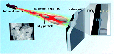 |
| | Fig. 1 A schematic depicting the supersonically expanded gas flow accelerating titania particles for the fabrication of a titania thin film as a photoelectrochemical anode. | |
2. Experimental
2.1. Preparation of the photoelectrode
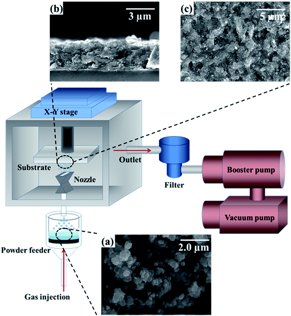
An indium-doped tin oxide (ITO)-coated glass was used as a substrate for TiO2 deposition. The detailed experimental setup for the AD technique is depicted in Fig. 2. This apparatus consists of a vacuum pump, booster pump, two-dimensional (2D) x–y stage, nozzle, fluidized-bed powder feeder, and gas tank. In AD, fine particles are dispersed in a carrier gas to generate a highly concentrated aerosol that is then accelerated to a high velocity at low pressure so that the particles are impacted on the target deposition surface with substantial kinetic energy.37–39 Table 1 summarizes the operating conditions of the AD experiment. The details of the supersonic flow are given in our previous studies.40,41 Fig. 2(a) shows the agglomerated TiO2 raw powder, which contain 60% anatase and 40% rutile by weight. These agglomerated clusters were pulverized by ball milling, which resulted in an average particle size of approximately 0.5 μm.42 Cross-sectional and plan-view SEM images of the as-deposited films are shown in Fig. 2(b) and (c), respectively. As reported in previous papers,43,44 the annealing of such films at 500 °C produces changes in surface roughness and enhances the crystallinity of the TiO2 thin-film samples. Thus, in the present study, the as-deposited films were annealed for one hour at 500 °C. Readers are referred to our previous publication for further details of the experimental setup.41
 |
| | Fig. 2 A schematic of the supersonic aerosol deposition technique. Insets include SEM images of (a) TiO2 powder from which films were deposited, and (b) side-view and (c) top-view of the as-deposited TiO2 films. | |
Table 1 Typical deposition conditions
| Pressure in deposition chamber [Torr] |
0.35–5.6 |
| Propellant gas |
Air |
| Nozzle exit area [mm2] |
10 × 35 |
| Stand-off distance [mm] |
5 |
| Gas temperature |
RT (20 °C) |
| Consumption of propellant gas [l min−1] |
10 |
| Stage traverse speed [mm s−1] |
0.72 |
| Number of passes |
1–4 |
2.2. Characterization of the photoelectrode
The surface microstructure of the films was characterized by scanning electron microscopy (HRSEM, XL30SFEG, Phillips Co., Holland, at 10 kV). The film thickness was measured by using the SEM images. For each measurement, data from five different SEM images were averaged. Powder X-ray diffraction (XRD, D/MAX-2500, Rigaku Japan with Cu Kα X-ray source) was used to analyze the crystal structure of the films. The diffraction peaks were recorded over the range of 20° < 2θ < 50°. Rietveld refinement of the powder diffraction patterns was carried out using the MAUD computer program.45 High-resolution transmission electron microscopy (HR-TEM, JEOL field-emission TEM (2100F) operated at 200 kV) was also used to characterize the nanostructure of the films. Surface morphology and surface roughness were analyzed by a non-contacting optical profiler (NT-1100, Veeco). Surface topographical images were taken under ambient laboratory conditions in air.
The film surface area was measured geometrically using atomic force microscopy (AFM, XE-100, Park System, Suwon, South Korea). AFM images were recorded over a 10 × 10 μm planar area in non-contact mode. A UV-Vis spectrophotometer (JASCO V-650, JASCO, Analytical Instruments, Tokyo, Japan, 200 ≤ λ ≤ 850 nm) was used to obtain absorbance and reflectance data. A common three-electrode system in a Teflon-covered glass vessel with AD TiO2 film as the photoelectrode (exposed area of ∼0.3 cm2), Ag/AgCl (in saturated KCl) as the reference electrode, and a platinum grid as the counter electrode was used for PEC measurements. The distance between these three electrodes was kept constant at 1 cm during each PEC measurement. A 1.0 M NaOH (Fluka Analytical, Sigma-Aldrich) solution was used as the electrolyte. During PEC measurements, the photoelectrode was exposed to 100 mW cm−2 illumination using a 400 W xenon arc lamp (Newport, Oriel Instruments, USA) as the light source. The light source was fitted with a water filter to absorb the IR region from the light and a UV short-pass filter (CVI, Melles Griot, Japan) was used to block light at wavelengths longer than 400 nm. The current–potential curves obtained from the photoelectrodes were recorded at a scan rate of 10 mV s−1 under dark and light conditions using a scanning potentiostat (VersaSTAT-3, Princeton Applied Research, USA).
2.3. Dye absorbance test
To estimate the relative abundance the pores and microcracks present in the films of different thickness and before and after annealing, dye absorbance tests were conducted. Both as-deposited and annealed films were soaked in a dye solution and then rinsed. The optical absorbance of the film and of the remaining dye solution was measured. The increased optical absorbance of the film, compared to the absorbance before dye adsorption, should be proportional to the amount of dye adsorbed. The amount of dye adsorbed should, in turn, be proportional to the total surface area accessible to the dye, including surface area within pores and micro-cracks, which would not be reflected in the AFM measurement.
The dye solution used was Ru(dcbpy)2(NCS)2 (N719, Solaronix) and had a concentration of 0.05 mM. The AD films were soaked with the dye solution and kept inside a dark box for 24 h so that dilution of the solution was affected only by the film adsorption and not by photodecomposition of the dye due to the ambient light. The remaining dye of each sample was collected and their absorbance was measured using a UV-Vis spectrophotometer. Absorbance of the films was also measured. The film surface was cleaned with DI water before measuring absorbance.
3. Results and discussion
3.1. Film crystallinity
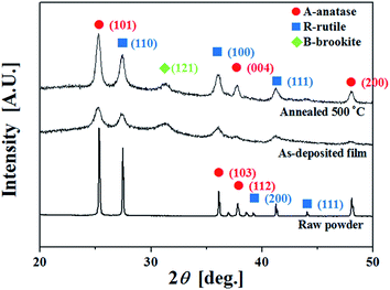
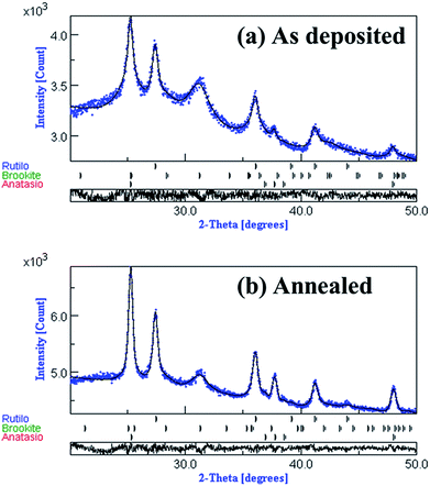
As previously reported,46 the crystallinity of aerosol deposited TiO2 films is greatly influenced by post-deposition annealing. Furthermore, the current experimental studies include the effect of film thickness on the photoelectrochemical performance, as summarized in Table 2. The crystal structure changes dramatically from the raw powder to the as-deposited film and then changes further upon annealing. The XRD peaks observed for the raw TiO2 powder and the 3 μm thick as-deposited and annealed TiO2 thin films are shown in Fig. 3 (which is Case 3 from Table 2). Fitting the XRD pattern of the raw powder gave phase fractions of approximately 54% anatase and 46% rutile, which is reasonably consistent with the manufacturer's specification of 60% anatase, 40% rutile. Fig. 3 shows that both as-deposited and annealed TiO2 films are polycrystalline. Peaks characteristic of anatase, rutile, and brookite phases are present. The XRD data of the raw powder indicates that the original powder did not contain any brookite. The peaks from the as-deposited film are of relatively modest intensity. These peaks intensified and became sharper after annealing at 500 °C. The (101), (004), and (200) planes of the anatase phase (JCPDS 21-1272) correspond to the peaks at 25.3°, 37.5°, and 48.1°. The (110), (100), and (111) planes of the rutile phase (JCPDS 21-1276) correspond to the peaks at 27.1°, 36.2°, and 41.1°. The peak at 31.7° can be assigned to the (121) crystal plane of the brookite phase (JCPDS 29-1360), which is evident in the as-deposited film. This peak intensified after annealing. Other peaks from the brookite phase overlap with those from anatase and rutile, but this (121) peak is unique to the brookite phase. After annealing, the intensities of the diffraction peaks corresponding to anatase, rutile, and brookite phases increased, indicating an increased degree of crystallinity and increased crystallite sizes in the TiO2 films upon heat treatment.
Table 2 Thickness, surface area, and roughness of the as-deposited and annealed AD films for Cases 1–4a
| |
As-deposited |
Annealed |
| Thickness [μm] |
Relative surface area |
Roughness [nm] |
Thickness [μm] |
Relative surface area |
Roughness [nm] |
| Relative surface area60: S3D/S2D ratio, S3D = surface area of sample by AFM, S2D = the surface area of the projection of 3D surface onto a film, i.e., the solid geometric area. |
| Case 1 |
0.5 |
1.19 |
230 |
0.4 |
1.04 |
160 |
| Case 2 |
1.5 |
1.22 |
280 |
1.4 |
1.19 |
210 |
| Case 3 |
3.0 |
1.24 |
320 |
2.5 |
1.20 |
275 |
| Case 4 |
4.0 |
1.29 |
360 |
3.4 |
1.22 |
310 |
 |
| | Fig. 3 The XRD patterns of raw powder and as-deposited and annealed TiO2 thin films for Case 3. | |
Fig. 4 shows the XRD results of the (a) as-deposited films and (b) the annealed films for various film thicknesses. In general, the annealed films are better crystallized, having relatively more distinct and sharper peaks. In addition, the thicker the film, the better the crystallization for both as-deposited and annealed cases. However, the ratio between the anatase and rutile peaks remains fairly constant between Case 3 and Case 4. Thus, there is no reason to further increase the film thickness beyond that of Case 3 in order to increase the concentration of the anatase phase, which plays the dominant role in the photocatalytic activity.
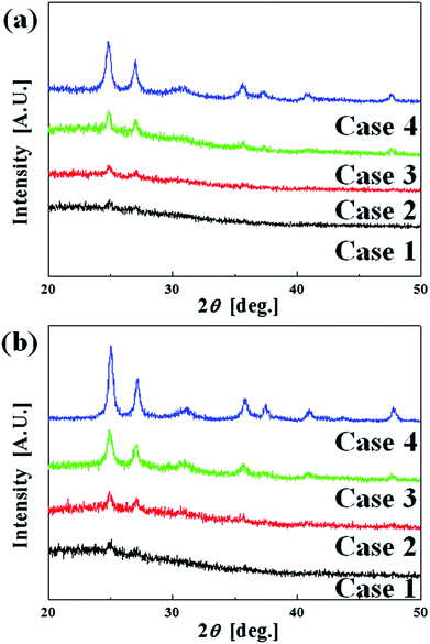 |
| | Fig. 4 The XRD results of the (a) as-deposited films and (b) the annealed films for various film thicknesses. | |
The diffraction patterns of the anatase, rutile, and brookite phases were fitted via Rietveld refinement to determine approximate phase fractions and crystallite sizes, as shown in the Fig. 5 and as summarized in Table 3. As expected, the brookite phase was not found in the raw powder. The small crystallite size and high strain in as-deposited films caused the wide and noisy characteristics of the XRD peaks. This is typical of films deposited by the aerosol deposition process, which fragments the original powder into smaller grains and has a propensity to build up high strain as a result of impacting fragments. In addition, the metastable brookite phase was produced by this high-energy impaction from the anatase and rutile phases, which are thermodynamically more stable than the brookite phase. Matching the XRD patterns of the films showed that the crystallite size for all three phases increased upon annealing and that the phase fraction of the metastable brookite phase decreased after annealing. Although the fitted phase fractions, crystallite sizes, and lattice parameters were not unique (i.e., several sets of parameters could give comparably good fits to the XRD pattern), all sets of fitted parameters supported these two trends. A crystalline semiconducting material contains many grains situated in various directions and separated by the grain boundaries. The degree of crystal structure perfection affects the overall electronic properties and hence the performance of the semiconductor photoelectrode.47 A more important factor may be the decrease in accessible surface area within the film that occurs upon annealing. The same mechanisms that led to the crystallite growth seen in the XRD patterns also led to the sintering of particles within the film, reducing the active surface area available for reaction. An analysis made by transmission electron microscopy (TEM), high-resolution TEM, and selected area electron diffraction (SAED) of the as-deposited and annealed films (Fig. 6) was consistent with the XRD results, showing nanoscale crystal domains within the film and increased crystallinity following annealing. It is also noteworthy that lattice fringes are clearly visible in the high-resolution TEM images in the lower-right corner of each image set.
 |
| | Fig. 5 XRD patterns with Rietveld refinement fits to a mixture of anatase, rutile, and brookite phases of Case 3. | |
Table 3 Results of Rietveld refinement fitting for Case 3
| Phase |
wt% |
Crystallite size (Å) |
Lattice parameter (Å) |
| a |
b |
c |
| (a) As deposited |
| Anatase |
10.4 |
271 |
3.792 |
|
9.542 |
| Brookite |
66 |
41 |
8.345 |
6.309 |
5.016 |
| Rutile |
23.6 |
173 |
4.600 |
|
2.961 |
| |
| (b) Annealed |
| Anatase |
25.2 |
420 |
3.787 |
|
9.528 |
| Brookite |
44.1 |
54 |
8.345 |
6.309 |
5.016 |
| Rutile |
30.7 |
260 |
4.597 |
|
2.96 |
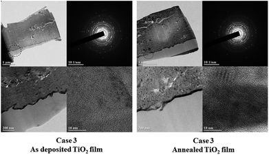 |
| | Fig. 6 TEM images of as deposited TiO2 film and annealed TiO2 film. The selected area diffraction patterns in the upper-right corner of each set of images show an increase in crystallinity (sharper pattern) after annealing, which is consistent with the XRD patterns of Fig. 3. Lattice fringes are clearly visible in the high-resolution TEM images in the lower-right corner of each image set. | |
3.2. Surface morphology and film thickness
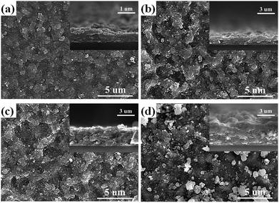
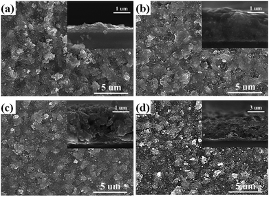
The supersonic aerosol deposition (AD) technique used here produced milky white films with four different nominal thicknesses (0.5, 1.5, 3, and 4 μm) as summarized in Table 2. The two-dimensional and cross-sectional SEM micrographs for the as-deposited and annealed (500 °C) TiO2 films of four thicknesses are shown in Fig. 7(a–d) and 8(a–d), respectively. The film thickness was reduced by 10–30% after annealing, as indicated in Table 2. This thickness reduction caused densification of the films, which in turn removed microcracks and pores that were present in the as-deposited films. In comparing Fig. 7 and 8, it is clear that all of the annealed TiO2 films appear to be denser than the as-deposited films.
 |
| | Fig. 7 The top-view and cross-sectional SEM images (in inset) of the as deposited TiO2 films for four different thicknesses, (a) Case 1, (b) Case 2, (c) Case 3, and (d) Case 4, respectively. | |
 |
| | Fig. 8 The top-view and cross-sectional SEM images (in inset) of the annealed TiO2 films for four different thicknesses, (a) Case 1, (b) Case 2, (c) Case 3, and (d) Case 4, respectively. | |
The microstructure of TiO2 film is generated by the collision of the accelerated TiO2 particles on the target substrate with high kinetic energy during aerosol deposition.48 During the impact of the TiO2 particles, the kinetic energy promotes adherence between the TiO2 particles and the target substrate. During the aerosol deposition process, TiO2 particles are more likely to adhere to previously deposited TiO2 particles, resulting in a highly roughened morphology. However, complete details of the deposition mechanism have not yet been fully clarified.49–51 The as-deposited AD TiO2 thin films consist of small, irregular grains with pores that extended throughout the bulk of the film. This existence of pores is consistent with our previous studies.52 However, the annealed films showed a more compact and dense morphology. The surface morphology of the thicker films was similar to that of thinner films. However, measurements from cross-sectional SEM images indicated a substantial decrease in film thickness after annealing (i.e., 10–30% reduction), from 0.5, 1.5, 3, and 4 μm to 0.4, 1.4, 2.5, and 3.4 μm, respectively.
Three-dimensional optical profilometry images of the as-deposited and annealed (500 °C) TiO2 films for Case 1–4 are shown in Fig. 9. The images were recorded over a 45 × 60 μm planar area in non-contact mode. The surface roughness (Ra) increased with increasing film thickness and decreased after annealing. The optical profiler studies revealed that the thinnest as-deposited and annealed TiO2 films had surface roughness values of 230 and 160 nm, respectively. The 1.5, 3, and 4 μm thick as-deposited TiO2 films had mean surface roughness values of 280, 320, and 360 nm, respectively. However, the surface roughness of the 1.4, 2.5, and 3.4 μm thick annealed TiO2 films decreased to 210, 275, and 310 nm, respectively. AFM images in Fig. 10 also show that all of the annealed films had reduced surface area and roughness, as summarized in Table 2. It is also noteworthy that both roughness and surface area increased with increasing film thickness from Case 1 to 4, which is typical of AD films.52 This change in the surface roughness can have a profound effect on light reflection which, in turn, affects the photoelectrochemical performance. Changes in reflectivity are discussed further below.
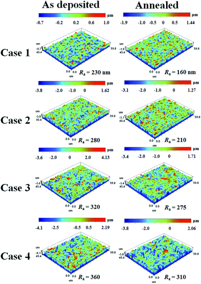 |
| | Fig. 9 The 3D optical profiler images of the as-deposited and annealed TiO2 films (scanning area = 45 × 60 μm). Figures in the left column are the as-deposited films for (a) Case 1, (b) Case 2, (c) Case 3, and (d) Case 4. Figures in the right column are the annealed films for (a) Case 1, (b) Case 2, (c) Case 3, and (d) Case 4. | |
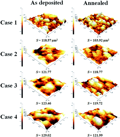 |
| | Fig. 10 AFM images of the as-deposited and annealed TiO2 films (scanning area = 10 × 10 μm). Figures in the left column are the as-deposited films for (a) Case 1, (b) Case 2, (c) Case 3, and (d) Case 4. Figures in the right column are the annealed films for (a) Case 1, (b) Case 2, (c) Case 3, and (d) Case 4. | |
3.3. Photoresponse
An important performance metric for water-splitting photoelectrodes is their stable photocurrent under illumination. We assume here that the photocurrent is maximal under the no loss condition and therefore, in an ideal scenario, the photocurrent directly corresponds to the rate of oxygen evolution.53 The effects of annealing on the TiO2 film thickness and on the resulting PEC performance were examined. Fig. 11 and 12 show the current–potential (I–V) graphs of the as-deposited and annealed films under illumination, respectively. Under UV illumination, the annealed TiO2 films showed quite low photocurrent density compared to the as-deposited TiO2 films. The photocurrent density of all TiO2 films started at approximately −0.9 V. It continued to increase and reached saturation at +0.2 V. In the case of the as-deposited TiO2 films (see Fig. 11), the photocurrent density at −0.2 V (corresponding to 1.23 VRHE) increased with increasing film thickness. At −0.2 V, the photocurrent density of the 0.5 μm thick TiO2 film was 19 μA cm−2 and the thicker 3 μm TiO2 film presented a photocurrent density of 93 μA cm−2 at −0.1 V. However, Case 4 showed a decrease in photocurrent density, to 65 μA cm−2. Although a similar trend was found for the annealed films (see Fig. 12), a dramatic decrease in photoresponse was observed for all of the annealed films. Apparently, any improvement in charge transport due to improved crystallinity after annealing was negligible as compared to these other effects.
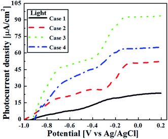 |
| | Fig. 11 The photoresponse of the as deposited TiO2 films with different thicknesses (Case 1–4) under light illumination. | |
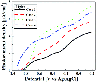 |
| | Fig. 12 The photoresponse of the annealed TiO2 films with different thicknesses (Case 1–4) under light illumination. | |
At 0.2 V, the photocurrent density of the annealed Case 1 was 1.7 μA cm−2 and the thicker annealed Case 3 had a photocurrent density of just 2.9 μA cm−2. The annealed Case 4 showed a lower photocurrent density of 1.8 μA cm−2. These photocurrent densities can be considered in light of results from the literature, but the PEC experimental details/conditions differ between studies, so the results are not always directly comparable. Fei et al. prepared 1 μm thick TiO2 (P25) thin films by spin-coating and observed a photocurrent density of nearly 100 μA cm−2 at −0.15 V.54 Morand et al. electrophoretically deposited mesoporous TiO2 films from colloidal suspensions of commercial TiO2 (P25) on interdigitated microelectrode arrays and achieved a photocurrent of nearly 70 μA at −0.3 V.55 Recently, Lee et al. compared the photocatalytic activities of commercial TiO2 (P25) and TiO2 nanorod-decorated graphene sheets prepared by non-hydrolytic sol–gel process under visible light irradiation. The TiO2 (P25) showed the photocurrent density of 0.41 mA cm−2 at +1.0 V, whereas, the TiO2 nanorod-decorated graphene sheets achieved the photocurrent density of 3.0 mA cm−2 at +1.0 V.56
As mentioned earlier, annealing caused film densification and roughness reduction, both of which contributed to the dramatic reduction in the photocurrent density. The film densification removed pores and microcracks that existed in the as-deposited films. These defects can have a positive effect on the photocurrent density by increasing the surface area. This increased photocatalytic activity of as-deposited film, compared to the annealed films, was also seen in our previous study of photocatalytic degradation of pollutants.52
The dramatic decrease in photoresponse observed after annealing was somewhat surprising; others have observed improved photoresponse after annealing of various photoelectrode materials.53,57,58 This difference results from the unique features of the supersonic AD film preparation method employed here. Supersonic AD produces partially fused nanoparticulate films directly with strong adhesion between nanoparticles and a relatively large contact area between particles. As a result, the as-deposited film can already provide charge transport pathways through the film. In a film deposited by spin-coating, dip-coating, or similar processes, only point contacts are made between particles. In that case, annealing results in slight sintering that can increase the area of contact between particles and improve charge transport through the film. The AD process also results in partial conversion of the starting TiO2 phase to the metastable brookite phase, which may be more active for photocatalysis compared to the anatase and rutile phases. Thus, the dominant effect of annealing the aerosol-deposited films is a reduction in surface area and reduction in brookite content, both of which reduce photocatalytic performance. The change in surface roughness also affects the reflectivity of the film, as discussed further below.
Changes in AD film thickness influence both light absorbance, by changing the optical path length and surface roughness, and the average distance over which photogenerated charge carriers must travel. These, in turn influence the charge separation and recombination processes in semiconductor photocatalysts.47 As the film thickness increased, more light was absorbed and reflected; transmittance was lower for the thicker films. However, once the film thickness exceeds the optical penetration depth for a given wavelength, further increases in thickness do not produce more absorbance at that wavelength, they only increase the distance that photogenerated electrons must travel before being collected. In general, for TiO2 films, high electron–hole recombination rates at the surface and grain boundaries diminish the photocurrent.59 In the present case, the highest photocurrent was obtained at a thickness of 3 μm (Case 3). Further increasing the film thickness resulted in decreased photoresponse, with effects of increased recombination and increased reflectance outweighing the effect of increased absorbance. This reversed trend in the photocurrent density observed from Case 3 to 4 is present for both as-deposited (Fig. 11) and annealed films (Fig. 12).
Fig. 13a compares absorbance of the as-deposited and annealed films. Overall, absorbance is greater for the as-deposited films than for the annealed films because of the microcracks and pores of the as-deposited films; the annealed films have greater transmittance, except for Case 3. Similarly, absorbance is higher for the thicker films for both as-deposited and annealed films. Fig. 13b compares total reflectance of the as-deposited and annealed films. In general, reflectance is higher for the annealed films, probably because of their increased crystallinity and larger crystallite size. As film thickness increased (from Case 1 to 4), the total reflectance increased because of the increased surface roughness, as shown in Fig. 7–10 and summarized in Table 2.
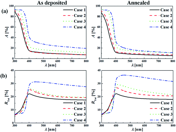 |
| | Fig. 13 UV-Vis (a) absorbance data and (b) total reflectance data for the as deposited TiO2 films and annealed TiO2 films. | |
Fig. 14 provides the results of a dye adsorption test, which provides another measure of the accessible surface area of the films. Films were soaked in a dye solution and adsorption of the dye was estimated by measuring the solution's absorbance. As shown in Fig. 14, absorbance of the dye solution is lower (transmittance is higher) for the solutions exposed to the as-deposited films. The as-deposited films absorbed more dye than the annealed films did. Note that the initial concentration of the dye solution for both as-deposited and annealed cases was set constant. In the as-deposited case, the thicker films (i.e., Case 3 and 4) absorbed more dye than thinner films, suggesting that internal surface area throughout the film is accessible to the dye.
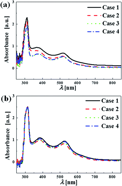 |
| | Fig. 14 Absorbance of the remaining dye solution after the film soaking for the (a) as-deposited and (b) annealed films. Discernable dilution (or higher transmittance) of the dye solution occurs if pores and microcracks are prevalent in the as-deposited in (a). | |
Fig. 15 shows the absorbance of the films after dye adsorption, while Fig. 14 showed that of the dye solution. Upon soaking in the dye solution, dye molecules are adsorbed on the walls of microcracks and pores, which would result in lower transmittance (or higher absorbance) of the film. Comparing the top and bottom figures of the as-deposited case (left), discernable dye adsorption indeed occurred with increased absorbance of the film. In particular, Case 3 shows the largest absorbance increase among all cases, which indicates that Case 3 had the largest accessible surface area, corresponding to its highest photocatalytic activity. As for the annealed case (right figures), dye adsorption was not significant as their absorbance remained fairly constant. This confirmed that pores and microcracks were eliminated during the annealing process, reducing the accessible surface area for catalysis.
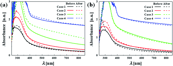 |
| | Fig. 15 Absorbance of the (a) as-deposited and (b) annealed films before and after the film soaking in the dye solution. | |
4. Conclusions
Supersonic aerosol deposition (AD) was employed to deposit nanostructured TiO2 films of varying thickness on ITO-coated glass substrates. Thicker AD films had a favorable photoelectrochemical performance because of increased interfacial area through microcracks and pores and increased path length for absorption. However, tradeoffs exist between the interfacial area and reflectance. High reflectance arising from the rougher surface of thicker films could adversely decrease the photocurrent density. Annealing caused densification of AD films and their photoelectrochemical performance was degraded. These results highlight the importance of surface microstructure and surface roughness in governing photoelectrode activity. The prepared TiO2 films were reproducible and stable during photoelectrochemical measurements. The performance achieved here in an otherwise un-optimized system suggests that supersonic AD may be a promising low-cost, high-throughput approach for producing water-splitting photoelectrodes, particularly on temperature-sensitive substrates.
Acknowledgements
This work was supported by the Industrial Strategic Technology Development Program (10045221), the Global Frontier R&D Program (2013-073298) on Center for Hybrid Interface Materials (HIM), and NRF-2013R1A2A2A05005589, and KETEP (20133030010890).
References
- J. M. Ogden, Annual Review of Energy and the Environment, 1999, 24, 227–279 CrossRef.
- Y. Li and J. Zhang, Laser Photonics Rev., 2010, 4, 517–528 CrossRef CAS.
- S. Dunn, Int. J. Hydrogen Energy, 2002, 27, 235–264 CrossRef CAS.
- B. C. Steele, Nature, 1999, 400, 619–621 CrossRef CAS PubMed.
- D. Aspnes and A. Heller, J. Phys. Chem., 1983, 87, 4919–4929 CrossRef CAS.
- P. V. Kamat, J. Phys. Chem. C, 2007, 111, 2834–2860 CAS.
- R. M. Navarro, M. C. Alvarez-Galván, J. A. V. de la Mano, S. M. Al-Zahrani and J. L. G. Fierro, Energy Environ. Sci., 2010, 3, 1865–1882 CAS.
- H. Tong, S. Ouyang, Y. Bi, N. Umezawa, M. Oshikiri and J. Ye, Adv. Mater., 2012, 24, 229–251 CrossRef CAS PubMed.
- F. E. Osterloh, Chem. Mater., 2007, 20, 35–54 CrossRef.
- J. Z. Zhang, MRS Bull., 2011, 36, 48–55 CrossRef CAS.
- T. Bak, J. Nowotny, M. Rekas and C. Sorrell, Int. J. Hydrogen Energy, 2002, 27, 991–1022 CrossRef CAS.
- A. Fujishima and K. Honda, Nature, 1972, 238, 37–38 CrossRef CAS.
- M. Anpo, S. Dohshi, M. Kitano, Y. Hu, M. Takeuchi and M. Matsuoka, Annu. Rev. Mater. Res., 2005, 35, 1–27 CrossRef CAS.
- I. D. Kim, A. Rothschild, D. J. Yang and H. L. Tuller, Sens. Actuators, B, 2008, 130, 9–13 CrossRef CAS PubMed.
- A. Nakajima, K. Hashimoto, T. Watanabe, K. Takai, G. Yamauchi and A. Fujishima, Langmuir, 2000, 16, 7044–7047 CrossRef CAS.
- R. Wang, K. Hashimoto, A. Fujishima, M. Chikuni, E. Kojima, A. Kitamura, M. Shimohigoshi and T. Watanabe, Nature, 1997, 388, 431–432 CrossRef CAS PubMed.
- B. O'Regan and M. Grfitzeli, Nature, 1991, 353, 737–740 CrossRef CAS.
- A. Fujishima, T. N. Rao and D. A. Tryk, J. Photochem. Photobiol., C, 2000, 1, 1–21 CrossRef CAS.
- A. Haarstrick, O. M. Kut and E. Heinzle, Environ. Sci. Technol., 1996, 30, 817–824 CrossRef CAS.
- K. Fujihara, T. Ohno and M. Matsumura, J. Chem. Soc., Faraday Trans., 1998, 94, 3705–3709 RSC.
- N. Patel, R. Fernandes, G. Guella, A. Kale, A. Miotello, B. Patton and C. Zanchetta, J. Phys. Chem. C, 2008, 112, 6968–6976 CAS.
- C. Y. Jimmy, W. Ho, J. Lin, H. Yip and P. K. Wong, Environ. Sci. Technol., 2003, 37, 2296–2301 CrossRef.
- H. Lin, Z. Xu, X. Wang, J. Long, W. Su, X. Fu and Q. Lin, J. Biomed. Mater. Res., Part B, 2008, 87, 425–431 CrossRef PubMed.
- P. Zeman and S. Takabayashi, Surf. Coat. Technol., 2002, 153, 93–99 CrossRef CAS.
- M. Abou-Helal and W. Seeber, Appl. Surf. Sci., 2002, 195, 53–62 CrossRef CAS.
- T. Oekermann, D. Zhang, T. Yoshida and H. Minoura, J. Phys. Chem. B, 2004, 108, 2227–2235 CrossRef CAS.
- R. C. Suciu, E. Indrea, T. D. Silipas, S. Dreve, M. C. Rosu, V. Popescu, G. Popescu and H. I. Nascu, J. Phys.: Conf. Ser., 2009, 182, 1–4 CrossRef.
- D. Dzibrou, A. Grishin, H. Kawasaki, Y. Suda and V. Pankov, J. Phys. Conf. Ser., 2008, 100, 1–4 CrossRef.
- R. S. Mane, W. J. Lee, H. M. Pathan and S.-H. Han, J. Phys. Chem. B, 2005, 109, 24254–24259 CrossRef CAS PubMed.
- S. C. Jung, B. H. Kim, S. J. Kim, N. Imaishi and Y. I. Cho, Chem. Vap. Deposition, 2005, 11, 137–141 CrossRef CAS.
- J. M. Macak, H. Tsuchiya and P. Schmuki, Angew. Chem., Int. Ed., 2005, 44, 2100–2102 CrossRef CAS PubMed.
- J. G. Yu, H. G. Yu, B. Cheng, X. J. Zhao, C. Y. Jimmy and W. K. Ho, J. Phys. Chem. B, 2003, 107, 13871–13879 CrossRef CAS.
- C.-W. Huang, C.-H. Liao and J. C. Wu, J. Clean Energy Technol., 2013, 1, 1–5 CAS.
- M. Kitano, M. Matsuoka, M. Ueshima and M. Anpo, Appl. Catal., A, 2007, 325, 1–14 CrossRef CAS PubMed.
- M. Anpo and M. Takeuchi, J. Catal., 2003, 216, 505–516 CrossRef CAS.
- M. Matsuoka, M. Kitano, M. Takeuchi, K. Tsujimaru, M. Anpo and J. M. Thomas, Catal. Today, 2007, 122, 51–61 CrossRef CAS PubMed.
- J. Ryu, J. J. Choi, B. D. Hahn, D. S. Park, W. H. Yoon and K. H. Kim, Appl. Phys. Lett., 2007, 90, 1–3 Search PubMed.
- J. J. Choi, J. H. Lee, D. S. Park, B. D. Hahn, W. H. Yoon and H. T. Lin, J. Am. Ceram. Soc., 2007, 90, 1926–1929 CrossRef CAS.
- J. J. Choi, B. D. Hahn, J. Ryu, W. H. Yoon and D. S. Park, J. Appl. Phys., 2007, 102, 1–6 Search PubMed.
- J. J. Park, M. W. Lee, S. S. Yoon, H. Y. Kim, S. C. James, S. D. Heister, S. Chandra, W. H. Yoon, D. S. Park and J. Ryu, J. Therm. Spray Technol., 2011, 20, 514–522 CrossRef CAS.
- M. Lee, J. Park, D. Kim, S. Yoon, H. Kim, D. Kim, S. James, S. Chandra, T. Coyle and J. Ryu, J. Aerosol Sci., 2011, 42, 771–780 CrossRef CAS PubMed.
- J. Akedo, J. Am. Ceram. Soc., 2006, 89, 1834–1839 CrossRef CAS.
- C. H. Heo, S.-B. Lee and J.-H. Boo, Thin Solid Films, 2005, 475, 183–188 CrossRef CAS PubMed.
- M. P. Neupane, I. S. Park, T. S. Bae, H. K. Yi, F. Watari and M. H. Lee, J. Electrochem. Soc., 2011, 158, C242–C245 CrossRef CAS PubMed.
- L. Lutterotti, Nucl. Instrum. Methods Phys. Res., Sect. B, 2010, 268, 334–340 CrossRef CAS PubMed.
- Y. Q. Hou, D. M. Zhuang, G. Zhang, M. Zhao and M. S. Wu, Appl. Surf. Sci., 2003, 218, 98–106 CrossRef.
- B. A. Pinaud, P. C. K. Vesborg and T. F. Jaramillo, J. Phys. Chem. C, 2012, 116, 15918–15924 CAS.
- J. Ryu, J. J. Choi, B. D. Hahn, D. S. Park, W. H. Yoon and K. H. Kim, Appl. Phys. Lett., 2007, 90, 2901 Search PubMed.
- J. Akedo, Mater. Sci. Forum, 2004, 449, 43–48 CrossRef.
- J. Ryu, D. S. Park, B. D. Hahn, J. J. Choi, W. H. Yoon, K. Y. Kim and H. S. Yun, Appl. Catal., B, 2008, 83, 1–7 CrossRef CAS PubMed.
- J. Ryu, B. Hahn, J. Choi, W. Yoon, B. Lee, J. Choi and D. Park, J. Am. Ceram. Soc., 2010, 93, 55–58 CrossRef CAS.
- J. J. Park, J. G. Lee, D. Y. Kim, J. H. Hong, J. J. Kim, S. Hong and S. S. Yoon, Environ. Sci. Technol., 2012, 46, 12510–12518 CrossRef CAS PubMed.
- I. Cesar, K. Sivula, A. Kay, R. Zboril and M. Grätzel, J. Phys. Chem. C, 2008, 113, 772–782 Search PubMed.
- H. Fei, Y. Yang, D. L. Rogow, X. Fan and S. R. Oliver, ACS Appl. Mater. Interfaces, 2010, 2, 974–979 CAS.
- R. Morand, C. Lopez, M. Koudelka-Hep, P. Kedzierzawski and J. Augustynski, J. Phys. Chem. B, 2002, 106, 7218–7224 CrossRef CAS.
- E. Lee, J. Y. Hong, H. Kang and J. Jang, J. Hazard. Mater., 2012, 219, 13–18 CrossRef PubMed.
- Q. Jia, K. Iwashina and A. Kudo, Proc. Natl. Acad. Sci. U. S. A., 2012, 109, 11564–11569 CrossRef CAS PubMed.
- K. Sivula, R. Zboril, F. Le Formal, R. Robert, A. Weidenkaff, J. Tucek, J. Frydrych and M. Gratzel, J. Am. Ceram. Soc., 2010, 132, 7436–7444 CrossRef CAS PubMed.
- J. A. Glasscock, P. R. Barnes, I. C. Plumb and N. Savvides, J. Phys. Chem. C, 2007, 111, 16477–16488 CAS.
- L. Stobiński and L. Zommer, Appl. Surf. Sci., 1998, 135, 8–14 CrossRef.
Footnote |
| † Equal contribution. |
|
| This journal is © The Royal Society of Chemistry 2014 |
Click here to see how this site uses Cookies. View our privacy policy here.