DOI:
10.1039/C3RA47130F
(Paper)
RSC Adv., 2014,
4, 6957-6964
Electronic band structure and specific features of AA- and AB-stacking of carbon nitride (C3N4): DFT calculation
Received
28th November 2013
, Accepted 3rd January 2014
First published on 6th January 2014
Abstract
The state-of-the-art all-electron full potential linear augmented plane wave based on density functional theory was applied for calculating the structural, electronic band structure, effective mass, density of state, and valence electron charge density of AA- and AB-stacking of carbon nitride (C3N4). Calculations were performed using four schemes, namely local density approximation (LDA-CA) by Ceperley–Alder, generalized gradient approximation developed by Perdew Burke and Ernzerhof (GGA-PBE), Engel–Vosko generalized gradient approximation (EV-GGA) and the recently developed modified Becke–Johnson (mBJ) potentials. The calculated band structure and total density of states verify the semiconducting nature of the two configurations with band gap of about 2.589 eV and 2.990 eV for AA- and AB-stacking of C3N4. The effective mass ratio of electron, heavy hole and light hole were calculated for both AA- and AB-stacking. The upper valence band in AB-stacking is much flatter as compared to AA-stacking, and elucidates a dramatic increase in the effective mass ratio of heavy holes which cause a reduction in group velocity of the wave packet and consequently decrease the mobility of the charge carrier. The partial density of state shows the variation in the orbital state and its strength as one moves from AA- to AB-stacking. The strong hybridization among the orbitals of both stacking (AA- and AB-) shows covalent nature of the bonds. The calculated valence electron charge density contour shows the prevailing covalent nature of C and N bonds with negligible percentage (8.08%) of ionicity.
1. Introduction
In recent years carbon nitride (C3N4) has attracteded considerable interest as a potential candidate for various biological and technological applications in biomedical, electronic, optical, mechanical and tribological applications.1–7 The C3N4 polymorph, with its high stability and reasonable band gap has been a fascinating research topic for theorists as well as experimentalists. Teter and Hemley4 have used the first principle pseudopotential calculation within the local density approximation (LDA) for calculating the structure and physical properties of carbon nitride polymorphs predict a cubic form of C3N4 with zero pressure bulk modulus exceeding that of diamond. Liu and Cohen5 have used an empirical model and an ab initio calculation to calculate the bulk moduli of β-C3N4, they found that β-C3N4 have compressibility as compared to diamond structure and the hardness of the compound was exposed to be more than diamond. Numerous theoretical and experimental studies were done on C3N4 polymorphs and its forms which focused on its preparation, electronic structure, elastic hardness, linear and nonlinear optical properties.8–35 Holst and Gillan35 synthesized the nitrogen rich carbon nitride network materials. Their investigations give clear idea about its use as photoactive materials. C3N4 is attractive organic semiconductor, gain considerable attention after Wang et al.36 described g-C3N4 as a metal free photocatalyst that can absorb more visible light, because of its band gap value (2.70 eV), produce hydrogen from water in comparison to the other oxides. It acquires admirable chemical stability, extraordinary optical characteristics and good thermal solidity that make it potential contestant as a photocatalyst for degradation under visible light. Recently Tahir et al.37 explored the electrochemical properties of tubular g-C3N4 which show high suitability as photocatalyst and supercapacitor used to clean environment and energy storage purpose. They highlighted further that improvement in the performance of g-C3N4 is due to its high surface area which include more active sites for reaction. The phenomenon of absorbing electromagnetic radiations is very important for photocatalyst, depends on the band gap of the material. Therefore it is necessary to know the accurate band gap's value of the material. Corkill and Cohen38 calculated the electronic band structure of β-C3N4 by GW approximation, they obtained a band gap of about 3.11 eV, in close agreement with the previous calculated band gap (3.20 eV) by Liu and Cohen.5 The electronic structure and optical properties of β-C3N4 were calculated by Yao and Ching.39 They observed that band gap of β-C3N4 linearly increases with increasing pressure. Ortega and Sankey40 calculated the electronic structure of the planer form of C3N4 (p-C3N4 and β-C3N4). They observed that relative stability of p-C3N4 and β-C3N4 and found that planer structure of p-C3N4 has lower total energy than β-C3N4 by at least 0.1 eV per atom. The calculated bulk modulus (189 GPa) of α-C3N4 exposed hardness of the reported compound to be approximately half of diamond while the predicted negative Poisson ratio of α-C3N4 also leads to fascinating application.41 We should emphasize that the pseudopotential hybrid functional (B3LYP) presented by Janesko42 and Wong and Cordaro43 is the correct way of solving the under-estimated band gaps that they observe in the nitride structures.
From above we noticed that most the reported work were done using non-full potential methods within LDA and GGA approaches. To the best of our knowledge no comprehensive first principles calculations based on full potential method were done for these materials. Therefore, we think it would be worthwhile to perform first-principles calculations, using the state-of-the-art all electron full-potential augmented plane wave plus local orbital approach (FP-APW+lo) based on the density functional theory (DFT) within four approximations namely; local density approximation (LDA-CA) by Ceperley–Alder, generalized gradient approximation developed by Perdew Burke and Ernzerhof (GGA-PBE), Engel–Vosko generalized gradient approximation (EV-GGA) and the recently developed modified Becke–Johnson (mBJ) potentials. Using four schemes for solving the exchange–correlation potentials give accurate result as compared to the previously used methods. This motivate us to carry out more advance computation of electronic band structure, density of states, effective mass and electronic charge density of the AA-stacking and AB-stacking of C3N4 using FPLAPW method which has proven to be one of the most precise technique within DFT to calculate the electronic structure of solids.44,45
2. Crystal structure and computational details
The crystal structure of AA- and AB-stacking of C3N4 as shown in Fig. 1a and b are stable in hexagonal symmetry with space group P![[6 with combining macron]](https://www.rsc.org/images/entities/char_0036_0304.gif) m2 (no. 187). The crystallographic data of C3N4 is taken from ref. 4. The state-of-the-art full-potential augmented plane wave plus local orbitals approach (FP-APW+lo) based on the density functional theory (DFT) within the framework of WIEN2K package46 was used. The self-consistent calculations were achieved using four schemes namely; LDA-CA,47 GGA-PBE,48 EV-GGA49 and recently developed mBJ scheme.50 LDA works sensibly well but has some shortcomings generally due to the tendency of over binding, which cause too small lattice constants. Perdew et al.48 added the gradient terms of the electron density to modify LDA to form a new approximation called generalized gradient approximation developed by Perdew Burke and Ernzerhof (GGA-PBE) which show accurate result in some cases. However both LDA and GGA-PBE have simplest forms that are not sufficiently flexible to accurately reproduce both the exchange–correlation energy and its charge derivative which generally underestimate the energy band gap.51 Engel and Vosko49 considered this deficiency and constructed a new functional form GGA called EV-GGA. Usually EV-GGA acquired by optimizing the exchange–correlation potential Vxc instead of the corresponding energy Exc. This approach yields better band splitting and structural properties that mainly depend on the accuracy of the exchange–correlation potential52,53 but still its results for narrow band gap materials and strongly correlated transition-metal compounds are not accurate. Furthermore the mBJ scheme was used.50 The mBJ, a modified Becke–Johnson potential, allows the calculation of band gaps with accuracy similar to the very expensive GW calculations.50 It is a local approximation to an atomic “exact-exchange” potential and a screening term. This format show best results not only for classical sp-type semiconductors, but also for strongly correlated transition-metal compounds.50 For the convergence of energy eigenvalues the wave function in the interstitial regions were expended in plane waves with cutoff RMTKmax = 7.0. Where RMT and Kmax stand for the muffin-tin (MT) sphere radius and magnitude of largest K vector in plane wave expansion, respectively. The chosen RMT is 1.24 atomic units (a.u.) for C and N atoms for both of AA- and AB-stacking. The wave function inside the sphere was expended up to lmax = 10 where as the Fourier expansion of the charge density was up to Gmax = 12(a.u.)−1. The self-consistent calculations are converged with the difference in total energy of the crystal did not exceed 10−5 Ryd for successive steps. The self consistent calculations were obtained for both cases by 308k points in irreducible Brillouin zone (IBZ).
m2 (no. 187). The crystallographic data of C3N4 is taken from ref. 4. The state-of-the-art full-potential augmented plane wave plus local orbitals approach (FP-APW+lo) based on the density functional theory (DFT) within the framework of WIEN2K package46 was used. The self-consistent calculations were achieved using four schemes namely; LDA-CA,47 GGA-PBE,48 EV-GGA49 and recently developed mBJ scheme.50 LDA works sensibly well but has some shortcomings generally due to the tendency of over binding, which cause too small lattice constants. Perdew et al.48 added the gradient terms of the electron density to modify LDA to form a new approximation called generalized gradient approximation developed by Perdew Burke and Ernzerhof (GGA-PBE) which show accurate result in some cases. However both LDA and GGA-PBE have simplest forms that are not sufficiently flexible to accurately reproduce both the exchange–correlation energy and its charge derivative which generally underestimate the energy band gap.51 Engel and Vosko49 considered this deficiency and constructed a new functional form GGA called EV-GGA. Usually EV-GGA acquired by optimizing the exchange–correlation potential Vxc instead of the corresponding energy Exc. This approach yields better band splitting and structural properties that mainly depend on the accuracy of the exchange–correlation potential52,53 but still its results for narrow band gap materials and strongly correlated transition-metal compounds are not accurate. Furthermore the mBJ scheme was used.50 The mBJ, a modified Becke–Johnson potential, allows the calculation of band gaps with accuracy similar to the very expensive GW calculations.50 It is a local approximation to an atomic “exact-exchange” potential and a screening term. This format show best results not only for classical sp-type semiconductors, but also for strongly correlated transition-metal compounds.50 For the convergence of energy eigenvalues the wave function in the interstitial regions were expended in plane waves with cutoff RMTKmax = 7.0. Where RMT and Kmax stand for the muffin-tin (MT) sphere radius and magnitude of largest K vector in plane wave expansion, respectively. The chosen RMT is 1.24 atomic units (a.u.) for C and N atoms for both of AA- and AB-stacking. The wave function inside the sphere was expended up to lmax = 10 where as the Fourier expansion of the charge density was up to Gmax = 12(a.u.)−1. The self-consistent calculations are converged with the difference in total energy of the crystal did not exceed 10−5 Ryd for successive steps. The self consistent calculations were obtained for both cases by 308k points in irreducible Brillouin zone (IBZ).
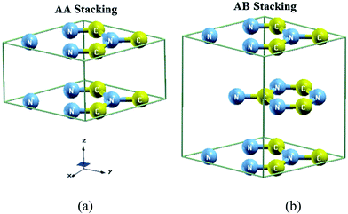 |
| | Fig. 1 Crystal structure of C3N4 unit call (a) AA-stacking (b) AB-stacking. | |
3. Results and discussion
3.1. Structural optimization
We have performed structural optimization by minimizing the energy with respect to unit cell volume of AA- and AB-stacking of C3N4. The exchange–correlation energy was treated by LDA-CA, GGA-PBE and EVGGA schemes to investigate the ground state properties. Fig. 2a–f represent energy verses volume plot for AA- and AB-stacking of C3N4 compound. The calculated total energies of C3N4 compound are fitted to the Murnaghan's equation of state54 to calculate the ground state properties:| |
 | (1) |
where E0, E0, B0 and B′0 represent ground state energy, volume, bulk modulus and pressure derivative of bulk modulus, respectively. The optimized ground state energy, volume, bulk modulus and pressure derivative of bulk modulus are shown in Table 1. The most stable structure is the one with the lowest total energy.55 Both Table 1 and Fig. 1a–f elucidates that EV-GGA show stable volume because of minimum value of the total energy among the other approximations (LDA and GGA). The optimized atomic positions of the investigated compound (AA- and AB-stacking of C3N4) are shown in Table 2.
 |
| | Fig. 2 Optimised energy vs. volume curve of C3N4 semiconductor. | |
Table 1 Present optimized parameters of C3N4 semiconductor
| |
AA-stacking |
AB-stacking |
| E0 (Ryd) |
V0 (a.u3) |
B0 (GPa) |
B′0 |
E0 (Ryd) |
V0 (a.u3) |
B0 (GPa) |
B′0 |
| LDA |
−661.853 |
437.3078 |
261.6851 |
3.8487 |
−1323.726 |
871.9735 |
262.7475 |
3.8393 |
| GGA |
−666.533 |
453.0975 |
239.7576 |
3.7503 |
−1333.044 |
903.5445 |
240.7553 |
3.7432 |
| EVGGA |
−672.213 |
495.9114 |
181.4819 |
4.0939 |
−3344.437 |
987.9344 |
193.7032 |
3.4704 |
Table 2 Present optimized atomic positions of C3N4 semiconductora
| |
Atomic coordinates |
| Atom |
X (Opt.)* |
Y (Opt.)* |
Z (Opt.)* |
| [Present work with GGA-PBE]*. |
| AA-stacking |
C1 |
0.686 |
0.843 |
0.000 |
| N1 |
0.333 |
0.666 |
0.000 |
| N2 |
0.835 |
0.164 |
0.000 |
| AB-stacking |
C1 |
0.018 |
0.509 |
0.500 |
| C2 |
0.686 |
0.843 |
0.000 |
| N1 |
0.666 |
0.333 |
0.500 |
| N2 |
0.333 |
0.666 |
0.000 |
| N3 |
0.168 |
0.831 |
0.500 |
| N4 |
0.835 |
0.164 |
0.000 |
3.2. Band structure
The importance of calculated band structure cannot be ignored for complete understanding the electronic structure and optical properties of the materials because most of the physical properties are directly or indirectly related to it and its basis are linked to the density of states. The energy band gap (Eg) of C3N4 is calculated by LDA-CA, GGA-PBE, EV-GGA and mBJ as shown in Table 3. The calculated electronic band structure of AA- and AB-stacking of C3N4 is shown in Fig. 3a and b. Following these figures and Table 3, we should emphasize that mBJ shows a better band gap, thus we have selected mBJ to demonstrate the electronic band structure as shown in Fig. 3c and d. The valence band maximum (VBM) and the conduction band minimum (CBM) of AA-stacking are located at A point of the BZ, resulting in a direct band gap. Whereas the VBM and the CBM of AB-stacking are shifted to be situated at the center of the BZ maintaining the direct band gap. The total density of states for AA- and AB-stacking of C3N4 are shown in Fig. 4a and b, these figures confirm our observation that mBJ exhibits better band splitting and hence better values of the energy gap.
Table 3 Calculated band gap and effective mass ratio of C3N4 semiconductor
| |
Energy gap |
| LDA |
GGA |
EVGGA |
mBJ |
| AA-stacking |
| Eg (eV) |
0.690 |
0.870 |
1.237 |
2.589 |
| m*e/me |
0.022 |
0.019 |
0.022 |
0.021 |
| m*hh/me |
0.108 |
0.111 |
0.143 |
0.154 |
| m*lh/me |
0.075 |
0.102 |
0.110 |
0.136 |
| |
| AB-stacking |
| Eg (eV) |
1.204 |
1.357 |
1.680 |
2.990 |
| m*e/me |
0.057 |
0.048 |
0.059 |
0.015 |
| m*hh/me |
1.840 |
1.406 |
1.324 |
6.773 |
| m*lh/me |
0.109 |
1.406 |
0.771 |
0.125 |
 |
| | Fig. 3 Calculated band structure of C3N4 semiconductor. | |
 |
| | Fig. 4 Calculated total and partial densities of states (States per eV unit cell). | |
3.3. Effective mass
The electron accelerated in periodic potential of the crystal in the presence of applied electric or magnetic field appear as effective mass (m*). The variation in effective mass of charge carrier depends on its location and energy in the band.56 The curvature of the energy band is inversely proportional to effective mass of the charge carrier. An electron moving near the top of allowed energy band acts like a negative mass. The effective mass of charge carrier is approximately equal to rest mass of electron close to the bottom of a nearly-free electron band, but there is considerable increases near the inflection point which turn out to be negative near the zone edge. Therefore the concept of “holes” is introduced in order to avoid the negative m*.56
The effective mass of the charge carrier, electron (m*e), heavy hole (m*hh) and light hole (m*lh) were calculated by fitting the dispersion curves around the A and Γ point of BZ following the expression;
| |
 | (2) |
or simply it can be written as
| |
 | (3) |
where
me symbolize the rest mass of electron. We calculated the effective mass ratio of electron (
m*e/
me) heavy hole (
m*hh/
me) and light hole (
m*lh/
me) using the conduction band minimum, upper valence band maximum and the lower valence band maximum. These values are shown in
Table 2. There is significant increase in calculated
m*hh/
me as one move from AA- to AB-stacking The upper valence band in AB-stacking is much flatter as compared to AA-stacking elucidates dramatic increase in the effective mass ratio of heavy holes which cause to reduce to group velocity of the wave packet and consequently decrease the mobility of the charge carrier.
3.4. Density of states
We have calculated the total and partial density of states (TDOS and PDOS) for AA- and AB-stacking of C3N4 using LDA, GGA, EVGGA and mBJ. The TDOS are presented in Fig. 4a and b. Following these figures and also from our prior experience which confirm that the mBJ scheme showed close agreement to the experimental results,57–63 therefore we have selected mBJ for advance explanation of partial density of state (PDOS). We hope that future experimental works will testify our calculated results. The partial density of states for AA- and AB-stacking of C3N4 is shown in Fig. 4c–f. In AA-stacking C-2s state show maximum peak (0.154 states per eV) around −13.5 eV, the same state in AB-stacking also show maximum peak with comparatively small density (0.146 states per eV). The next dominant peak of C-2s in both stacking located around −11.0 eV with same density (0.075 states per eV). As one move towards higher energy, the contribution of C-2s decreases which become very small in the valence band. Its contribution in lower conduction bands is almost zero which again becomes foremost from 6.8 eV to 15.0 eV for both stacking. The first peak of C-2s in the conduction band around 8.0 eV in AA-stacking is about 0.08 states per eV which increases to be 0.10 states per eV for AB-stacking. N-2s state show completely different behaviors for AA- and AB-stacking. There are three dominant peaks in AA-stacking around −13.5, −4.6 and −0.1 eV which shows maximum value of 0.07, 0.05 and 0.08 (states per eV) whereas AB-stacking shows maximum peak of about (0.11 states per eV) around −11.0 eV while N-2s play negligible role in energy range between −11.0 eV and Fermi level. In the conduction band N-2s state show maximum peak (0.05 states per eV) for AA-stacking around 8.0 eV. In case of AB-stacking N-2s state shift towards 7.5 eV with increasing the peak heights to be 0.21 states per eV.
Similarly C-2s/2p and N-2s/2p states show dominant contribution in bands formation. In AA-stacking C-2p state around −7.5 eV is dominant with peak heights of about (0.3 states per eV) which gradually decreases and become zero at Fermi level. The remaining range shows two prevailing peaks around 2.5 eV and 8.0 eV with maximum value of 0.18 states per eV and 0.25 states per eV. In AB-stacking C-2p show dominancy around −7.5 eV and 3.5 eV with the value of 0.28 states per eV and0.45 states per eV. N-2p state play the leading role in bands formation especially in valence band of both stacking. For AA-stacking the first dominant peak is located around −7.5 eV with the value of 0.24 states per eV which increase to be 0.56 states per eV. In AB-stacking the density of the first peak increased to 0.73 states per eV and the second dominant peak is shifted from Fermi energy to −2.0 eV with0.5 states per eV. The contribution of N-2p in conduction band is same as that of C-2p state. From −7.0 eV to Fermi level the N-2p state is dominant and play major role in formation of valence band for AA-stacking. The conduction band is mainly formed by hybridized C-2p and N-2p. In AB-stacking the valence band is fashioned by hybridized C-2p and N-2p with small part of C-2s and N-2s and the conduction band is mainly formed by C-2p.
One can also see strong hybridization between C-2s and N-2s, C-2p and N-2p states. We should emphasize that the strong hybridization among C-s/p state and N-s/p result covalent nature of the bond which can be observed in electronic charge density contour.
3.5. Electronic charge density
The bonding nature can be accurately explained on the base of electronic charge density plot which is derived from the reliable converge wave function.64,65 We have calculated the valence charge density in (001) plane for AA- and AB-stacking C3N4 by four schemes LDA-CA, GGA-PBE, EVGGA and mBJ-GGA but the results of these formats of exchange correlation potential were almost same, therefore we showed the results of mBJ format which perfectly describe the bonding nature and charge transfer as shown in Fig. 5a and b. We have calculated the electronic charge density of top layer along 2 × 2 × 1 directions in order to completely visualize the bonding nature of the hexagon. The blue color shows the maximum charge intensity as shown in scale while the red color represents zero charge density regions. The blue region in the hexagon representing strong sharing of charge between C and N atom which results the dominant covalent bond among the constituents in the given layer. One can also observe the bonding nature and percentage ionicity by using Pauling scale and Pauling empirical formula used in ref. 66. The electro-negativity difference between C (2.55) and N (3.04) elucidates non polar covalent bond with 8.68% of ionicity.
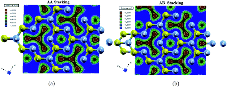 |
| | Fig. 5 Electronic charge density contour of C3N4 in (001) plane (a) AA-stacking (b) AB-stacking. | |
4. Conclusions
We have calculated the electronic band structure, density of state and electronic charge density of AA- and AB-stacking carbon nitride (C3N4) using all electron full potential linear augmented plane wave (FPLAPW) method based on DFT within the frame work of Wien2k code. The mBJ potential was preferred due to better band gap for both AA- and AB-stacking in comparison to LDA-CA, GGA-PBE and EV-GGA schemes. The calculated band structures and partial density of states (PDOS) for AA- and AB-stacking were calculated and discussed in details. The calculated effective mass ratio of electron, heavy hole and light hole show variation with bands curvature of AA- and AB-stacking, respectively. The calculated PDOS shows the variation in the states when one move from AA- to AB- stacking. The strong hybridization between C-2s/2p state and N-2s/2p state in AA- and AB-stacking results covalent nature of the bond. The valence electron charge density calculated for both stacking (AA and AB) in (001) plane along 2 × 2 × 1 directions elucidates covalent nature of C and N bond with 8.08% of ionicity.
Acknowledgements
The result was developed within the CENTEM project, reg. no. CZ.1.05/2.1.00/03.0088, co-funded by the ERDF as part of the Ministry of Education, Youth and Sports OP RDI programme. SA would like to thank CSIR-NPL for financial support.
References
- E. Kroke and M. Schwarz, Coord. Chem. Rev., 2004, 248, 493 CrossRef CAS PubMed.
- M. H. V. Huynh, M. A. Hiskey, J. G. Archuleta and E. L. Roemer, Angew. Chem., Int. Ed., 2004, 43, 5658 (Angew. Chem., Int. Ed., 2005, 44, 737) CrossRef CAS PubMed.
- L. C. Ming, P. Zinin, Y. Meng, X. R. Liu, S. M. Hong and Y. Xie, J. Appl. Phys., 2006, 99, 033520 CrossRef PubMed.
- D. M. Teter and R. J. Hemley, Science, 1996, 271, 53 CAS.
-
(a) A. Y. Liu and M. L. Cohen, Science, 1989, 245, 841 CAS;
(b) A. Y. Liu and M. L. Cohen, Phys. Rev. B: Condens. Matter Mater. Phys., 1990, 41, 10727 CrossRef CAS.
- Q. Lv, C. B. Cao, C. Li, J. T. Zhang, H. S. Zhu, X. Kong and X. F. Duan, J. Mater. Chem., 2003, 13, 1241 RSC.
- D. R. Miller, D. C. Swenson and E. G. Gillan, J. Am. Chem. Soc., 2004, 126, 5372 CrossRef CAS PubMed.
- T. Sekine, H. Kanda, Y. Bando, M. Yokohama and K. Hojou, J. Mater. Sci. Lett., 1990, 9, 1376 CrossRef CAS.
- L. Maya, D. R. Cole and E. W. Hagaman, J. Am. Ceram. Soc., 1991, 74, 1686 CrossRef CAS.
- M. Wixom, J. Am. Ceram. Soc., 1990, 73, 1973 CrossRef CAS.
- J. J. Cuomo, P. A. Leary, D. Yu, W. Reuter and M. Frisch, J. Vac. Sci. Technol., 1976, 16, 299 CrossRef.
- H. X. Han and B. J. Feldman, Solid State Commun., 1988, 65, 921 CrossRef CAS.
- C. Niu, Y. Z. Liu and C. M. Lieber, Science, 1993, 261, 334 CAS.
- D. Marton, K. J. Boyd, A. H. Al-Bayati, S. S. Todorov and J. W. RABlais, Phys. Rev. Lett., 1994, 73, 118 CrossRef CAS.
- K. M. Yu, M. L. Cohen, E. E. Haller, W. L. Hansen, A. Y. Lu and L. C. Wu, Phys. Rev. B: Condens. Matter Mater. Phys., 1994, 49, 5034 CrossRef CAS.
- J. P. Riviere, D. Texier, J. Delafond, M. Jaouen, E. L. Mathe and J. Chaumont, Mater. Lett., 1995, 22, 115 CrossRef CAS.
- Z. M. Ren, et al., Phys. Rev. B: Condens. Matter Mater. Phys., 1995, 51, 5274 CrossRef CAS.
- Y. Yang, K. A. Nelson and F. Adibi, J. Mater. Res., 1995, 10, 41 CrossRef CAS.
- H. R. Phillip and E. A. Taft, Phys. Rev., 1964, 136, A1445 CrossRef.
- P. Kroll and R. Hoffmann, J. Am. Chem. Soc., 1999, 121, 4696 CrossRef CAS.
- H. Yao and W. Y. Ching, Phys. Rev. B: Condens. Matter Mater. Phys., 1994, 50, 11231 CrossRef CAS.
- J. Ortegaand and O. F. Sankey, Phys. Rev. B: Condens. Matter Mater. Phys., 1995, 51, 2624 CrossRef.
- M. R. Wixom, J. Am. Ceram. Soc., 1996, 73, 1973 CrossRef.
- J. E. Lowther, Phys. Rev. B: Condens. Matter Mater. Phys., 1998, 57, 5724 CrossRef CAS.
- S.-D. Mo, L. Ouyang and W. Y. Ching, Phys. Rev. Lett., 1999, 83, 5046 CrossRef CAS.
- G.-M. Rignanese, J.-C. Charlier and X. Gonze, Phys. Rev. B: Condens. Matter Mater. Phys., 2002, 66, 205416 CrossRef.
- M. Marqués, J. Osorio, R. Ahuja, M. Flórez and J. M. Recio, Phys. Rev. B: Condens. Matter Mater. Phys., 2004, 70, 104114 CrossRef.
- Y. Zhang, H. Sun and C. Chen, Phys. Rev. B: Condens. Matter Mater. Phys., 2006, 73, 064109 CrossRef.
- J. He, L. Guo, X. Guo, R. Liu, Y. Tian, H. Wang and C. Gao, Appl. Phys. Lett., 2006, 88, 101906 CrossRef PubMed.
- J. Hu, W. Cheng, S. Huang, D. Wu and Z. Xie, Appl. Phys. Lett., 2006, 89, 261117 CrossRef PubMed.
- I. Alves, G. Demazeau, B. Tanguy and F. Weill, Solid State Commun., 1999, 109, 697 CrossRef CAS.
- M. Mattesini, S. F. Matar and J. Etourneau, J. Mater. Chem., 2000, 10, 709 RSC.
- E. Kroke, M. Schwarz, E. Horath-Bordon, P. Kroll, B. Noll and A. D. Norman, New J. Chem., 2002, 26, 508 RSC.
- J. Gracia and P. Kroll, J. Mater. Chem., 2009, 19, 3013 RSC.
- J. R. Holst and E. G. Gillan, J. Am. Chem. Soc., 2008, 130, 7373 CrossRef CAS PubMed.
- X. C. Wang, K. Maeda, A. Thomas, K. Takanabe, G. Xin, J. M. Carlsson, K. Domen and M. Antonietti, Nat. Mater., 2009, 8, 76 CrossRef CAS PubMed.
- M. Tahir, C. Cao, F. K. Butt, F. Idrees, N. Mahmood, I. Aslam, Z. Ali, M. Tanvir, M. Rizwan and T. Mahmood, J. Mater. Chem. A, 2013, 1, 13949 CAS.
- J. L. Corkill and M. L. Cohen, Phys. Rev. B: Condens. Matter Mater. Phys., 1993, 48, 17622 CrossRef CAS.
- H. Yao and W. Y. Ching, Phys. Rev. B: Condens. Matter Mater. Phys., 1994, 50, 11231 CrossRef CAS.
- J. Ortega and O. F. Sankey, Phys. Rev. B: Condens. Matter Mater. Phys., 1995, 51, 2624 CrossRef CAS.
- Y. Guo and W. A. Goddard, Chem. Phys. Lett., 1995, 237, 72 CrossRef CAS.
- B. G. Janesko, J. Chem. Phys., 2011, 134, 184105 CrossRef PubMed.
- B. M. Wong and J. G. Cordaro, J. Phys. Chem. C, 2011, 115, 18333 CAS.
- S. Gao, Comput. Phys. Commun., 2003, 153, 190 CrossRef CAS.
- K. Schwarz, J. Solid State Chem., 2003, 176, 319 CrossRef CAS.
- P. Balaha, K. Shewartz, G. K. H. Madsen, D. Kvsnicka and J. Luitz, WIEN2K, an Augmented plane wave + local orbitals program for calculating crystals properties,Karlheinz Schewartz, Techn. Universitat, Wien Austria, 2001, ISBN 3-9501031-1-2 Search PubMed.
- D. M. Ceperley and B. I. Alder, Phys. Rev. Lett., 1980, 45, 566 CrossRef CAS.
- J. P. Perdew, K. Burke and M. Ernzerhof, Phys. Rev. Lett., 1996, 77, 3865 CrossRef CAS.
- E. Engel and S. H. Vosko, Phys. Rev. B: Condens. Matter Mater. Phys., 1993, 47, 13164 CrossRef CAS.
- F. Tran and P. Blaha, Phys. Rev. Lett., 2009, 102, 226401 CrossRef.
- P. Dufek, P. Blaha and K. Schwarz, Phys. Rev. B: Condens. Matter Mater. Phys., 1994, 50, 7279 CrossRef CAS.
- Z. Charifi, H. Baaziz and A. H. Reshak, Phys. Status Solidi B, 2007, 244(9), 3154 CrossRef CAS.
- A. H. Reshak, Z. Charifi and H. Baaziz, Eur. Phys. J. B, 2007, 60, 463 CrossRef CAS.
- F. D. Murnaghan, Proc. Natl. Acad. Sci. U. S. A., 1944, 30, 244 CrossRef CAS.
- M. Zhou, Y.-H. Lu, Y.-Q. Cai, C. Zhang and Y.-P. Feng, Nanotechnology, 2011, 22, 385502 CrossRef PubMed.
- A. P. Hibbins, PHY3102/3305 Solid State Physics I – 2009/10.
- A. H. Reshak, X. Chen, S. Auluck and H. Kamarudin, Mater. Chem. Phys., 2012, 137, 346 CrossRef CAS PubMed.
- A. H. Reshak, X. Chen, S. Auluck and H. Kamarudin, J. Appl. Phys., 2012, 112, 053526 CrossRef PubMed.
- A. H. Reshak, I. V. Kityk, O. V. Parasyuk, A. O. Fedorchuk, Z. A. Alahmed, N. AlZayed, H. Kamarudin and S. Auluck, J. Mater. Sci., 2013, 48, 1342 CrossRef CAS.
- A. H. Reshak and S. A. Khan, Mater. Res. Bull., 2013, 48, 4555 CrossRef CAS PubMed.
- M. Benkraouda and N. Amrane, J. Alloys Compd., 2013, 546, 151 CrossRef CAS PubMed.
- S.-D. Guo and B.-G. Liu, J. Magn. Magn. Mater., 2012, 324, 2410 CrossRef CAS PubMed.
- H. Hakan Gürel, Ö. Akinci and H. Ünlü, Superlattices Microstruct., 2012, 51, 725 CrossRef PubMed.
- R. Hoffman, Rev. Mod. Phys., 1988, 60, 601 CrossRef.
- C. D. Gellatt, A. R. Willaims Jr and V. L. Moruzzi, Phys. Rev. B: Condens. Matter Mater. Phys., 1983, 27, 2005 CrossRef.
- Schlusseltechnologien Key Technologies, 41st IFF Springschool, 2010, p. A1.18 Search PubMed.
|
| This journal is © The Royal Society of Chemistry 2014 |
Click here to see how this site uses Cookies. View our privacy policy here.