Synthesis and characterization of nanoporous Bi3NbO7 films: application to photoelectrochemical water splitting

Jiangang Jiang , Meng Wang , Qingyun Chen *, Shaohua Shen , Mingtao Li and Liejin Guo
State Key Laboratory of Multiphase Flow in Power Engineering, The International Research Center of Renewable Energy, Xi'an Jiaotong University, Shaanxi 710049, P.R. China. E-mail: jjg2100@163.com; qychen@mail.xjtu.edu.cn

Received 29th November 2013 , Accepted 30th January 2014

First published on 31st January 2014


Abstract

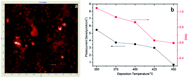
Nanostructured Bi3NbO7 films were successfully prepared via an ultrasonic spray pyrolysis method by using Bi(NO3)3·5H2O and Nb2O5 as precursors. The as-prepared films were systematically characterized by X-ray diffraction, Atomic Force Microscopy (AFM), field emission scanning electron microscopy (FESEM), UV-vis absorption spectra and X-ray photoelectron spectroscopy. The characterization results revealed that the nanostructured Bi3NbO7 possessed a cubic structure, nanoporous morphology and a visible light absorption with an optical band gap of about 2.8 eV. Moreover, electrochemical and photoelectrochemical measurements were carried out and a maximum photocurrent density of 2.8 μA cm−2 at the potential of 0.7 V vs. SCE was obtained for the Bi3NbO7 film deposited at 350 °C. The improvement of the film photoelectrochemical properties was contributed by novel nanoporous morphology that supply sufficient electrode–solution contact area. By addition of methanol into the solution, the photocurrent increased by 60%. The photoelectrochemical results reveal that the prepared films have the potential for hydrogen production via splitting water.


1. Introduction

Photoelectrochemical (PEC) water splitting for hydrogen production has been gaining intense attention because of its potential application in solar energy conversion and utilization.1,2 Many kinds of semiconductor materials, such as TiO2, BiVO4, Cd1−xZnxS, and ZnIn2S4,3–7 were introduced for the purpose of efficiently splitting water for hydrogen production. However, TiO2 absorbs only UV light because of its large band gap, while for the visible light response materials, like Cd1−xZnxS and ZnIn2S4, stability is poor in the PEC reaction due to photocorrosion.12 So they are not appropriate for efficient PEC water splitting. Niobates were studied by numerous researchers for their high photocatalytic activity and anticorrosion properties. For example, ANb2O6 (A = Ca, Sr, Ba)8 and MLaSrNb2NiO9 (M = Na, Cs, H)9 showed good photocatalytic activity due to their unique octahedral structure and d0 electronic configuration. Bi3NbO7 is a visible light semiconductor and bismuth is considered to be non-toxic and noncarcinogenic.10 However, the bismuth niobate as a photocatalyst for hydrogen production was rarely studied, especially Bi3NbO7 photoelectrode for PEC water splitting.

Niobates were conventionally synthesized by high temperature solid-state method, which required of harsh condition of high temperature (above 1000 °C).11–17 In addition, film based on PEC for hydrogen production from water splitting require a film electrode with large roughness factor to increase electrode–solution area. Recently, nanostructure (like nanorod, nanotube, nanoflower, mesoporous etc.) have been developed for their potential improvement PEC properties of semiconductor materials due to their high surface area and size dependent property.18–22 In this paper, nanoporous Bi3NbO7 thin films were prepared by ultrasonic spray pyrolysis method at low temperature. This novel film electrode showed extremely large roughness factor and then improved PEC properties of film electrodes.

Spray pyrolysis23 as a convenient, fast and economical technique was widely used to prepare powders and films. It is easy to control the stoichiometric ratio of the synthesized films by adjusting the composition of precursor solutions. Furthermore, this method is easy to scale up for large area film preparation. However, this method needs dissoluble salt as the precursor, which is a big challenge for niobates because of its poor dissolubility in water. In this paper, a novel method to dissolve the niobate at low temperature was introduced in detail and a novel nanoporous Bi3NbO7 film was prepared by spray pyrolysis method. The crystal structure, PEC and electrochemical properties were characterized. These Bi3NbO7 films were found to display effective PEC performance in water splitting.

2. Experiments

2.1. Preparation of films

All the chemicals used in the experiment were of analytical grade without further purification. Citric acid and ethylene glycol were used as the chelate and esterifiable reagents, respectively. Deionized water was used throughout the experiment.

There are three steps to prepare the Bi3NbO7 films by ultrasonic spray pyrolysis method and the preparation flowchart is shown in Fig. 1. The first step was to prepare the solution (A) containing Nb ions: Nb2O5 and NaOH were mixed with a stoichiometric ratio 1[thin space (1/6-em)]:[thin space (1/6-em)]4 and annealed for 4 h in a muffle furnace at 400 °C to form Na3NbO4 powder. Then Na3NbO4 powder was dissolved in the deionized water and filtrated. Acetic acid was added slowly into the above filtrate and the white floccules were formed which was made up of Nb(OH)5. The dried Nb(OH)5 was dissolved in the ethylene glycol(EG) using citric acid as chelate agent.24 Then deionized water was added into the mixture to form a 0.005 M [Nb5+] solution denoted as A. The chemical reactions occurred in the process are shown below

 
Nb2O5 + 6NaOH = 2Na3NbO4 + 3H2O(1)
 
6Na3NbO4 + 5H2O = 18Na+ + Nb6O198− + OH(2)
 
4Na+ + Nb6O198− + 8H+ + 4OH = Na4H4Nb6O19↓ + 4H2O(3)
 
Na4H4Nb6O19 + 15H+ + 11OH = 6Nb(OH)5↓ + 4Na+(4)


image file: c3ra47118g-f1.tif
Fig. 1 Flowchart of the preparation of Bi3NbO7 film.

The second step was to prepare the solution (B) with Bi ions: Bi(NO3)3·5H2O was dissolved in dilute nitric acid under stirring. Then certain amount ethylenediaminetetraacetic acid (EDTA)-ammonia solution was added to bismuth nitrate solution to make [Bi3+] 0.02 M and denoted the solution as B. The third step was to prepare the Bi–Nb precursory solution: the solutions (A) and (B) were mixed together in the volume ratio of 4[thin space (1/6-em)]:[thin space (1/6-em)]3. The Bi3NbO7 films were deposited on the In-doped SnO2 coated glass (ITO) substrate by ultrasonic spray pyrolysis method at temperatures of 350 °C, 375 °C, 400 °C, 425 °C and 450 °C and these films were denoted as 350 °C, 375 °C, 400 °C, 425 °C and 450 °C respectively. After the deposition, all the films were annealed at 500 °C for 2 h to remove the organic remains and improve their crystalline. In order to investigate film thickness effect on its property, the previous spray pyrolysis procedure was repeated 1, 2, 3, 4, 5 and 6 times at 350 °C and corresponding film was denoted as 1, 2, 3, 4, 5 and 6.

2.2. Film characterization

The structural properties of the prepared films were characterized by X-ray diffraction (PANalytical, using Cu Kα irradiation λ = 15.4184 nm) operated at 40 kV and 40 mA. The morphology of the films was observed using an Atomic Force Microscope (AFM, Solve Next) and field emission scanning electron microscopy (FESEM, JSM-6700F), and the film formation was examined by X-ray photo-electron spectroscope (XPS, AXIS-ULTRA). Optical absorption spectra were recorded using a double-beam UV4100 UV-vis-NIR spectrophotometer equipment.

2.3. PEC Measurements

Electrochemical and PEC measurements were carried out in a convenient three electrodes cell using a potentiostat (273A from Princeton Applied Research Company). The ITO/Bi3NbO7 films were cut into 1 cm × 1 cm squares as working electrode. A Pt plate was used as counter electrode and a saturated calomel electrode (SCE) as reference electrode. A 0.5 M Na2SO4 aqueous solution was employed as electrolyte solution. The light source was a Xe lamp (350 W) without any filters and its intensity was 150 mW cm−2 measured by an irradiatometer. For all the measurements, the irradiated area of working electrode was fixed at 0.785 cm2.

3. Results and discussion

3.1 Structure and morphology analysis

XRD was used to determine the crystal structure and phase composition of the samples. XRD patterns of Bi3NbO7 films deposited at temperature of 350 °C, 375 °C, 400 °C, 425 °C and 450 °C, respectively, are shown in Fig. 2. From Fig. 2, it can be seen that the diffraction peaks of Bi3NbO7 film deposited at 350 °C are ascribed to the Bi3NbO7 cubic structure (JCPDS 089–5564). The five peaks in the patterns are well indexed to (1 1 1), (2 0 0), (2 2 0), (3 1 1) and (2 2 2) facet in angle order. With increasing the deposition temperature, the diffraction peaks attributed to ITO appear. These peaks are marked by asterisk, which was resulted from the ITO substrate. With the increase of substrate temperatures, the mass of spray droplets arrived at substrate decreased gradually, contributing to the decreasing thickness of the Bi3NbO7 films. Therefore, the thickness of film became thinner as the substrate temperatures increased, and almost disappeared at 450 °C. Therefore, the XRD diffraction peaks of Bi3NbO7 film synthesized at high temperatures (450 °C) were not observed. Furthermore, no other impurity peak is found, which indicates that the prepared films consist of the single phase of cubic Bi3NbO7 under low deposition temperature.
image file: c3ra47118g-f2.tif
Fig. 2 The XRD patterns of Bi3NbO7 films and ITO at various temperatures (* is ITO peak).

Scanning electron microscopy (SEM) and Atomic force microscopy (AFM) images were collected for the Bi3NbO7 films prepared with different deposition temperature in order to understand the correlation of this parameter to the sample morphology. Fig. 3 shows the SEM and AFM images for the deposited films. Under low resolution SEM images, the spherical particles can be seen at the deposition temperatures of 350 °C, 375 °C, 400 °C, 425 °C and 450 °C. And the diameters of the spherical particles decreased with increasing deposition temperature, from 30 μm (350 °C) to 20 μm (425 °C). Furthermore, nanoporous structure was observed in all films with a typical porous size of about 40 nm at the deposition temperature of 350 °C. When the deposition temperature was elevated to 450 °C, the porosity was decreased and the porous size was decreased comparing to that deposited at lower temperature. This structure of spherical particles and nanoporous can increase contact area between film and electrolyte. As been widely accepted, photoelectrode requires a high surface area, and increasing the contact area between film and electrolyte will enhance its photocatalytic activity.25,26 Therefore, this structure of spherical particles and nanoporous structure may give a high photocurrent density and efficiency. Fig. 3(e) reveals that the thickness of film deposited at 350 °C is increased with repeating times increasing, which is consistent with our expected. The AFM image of Fig. 3(f) shows the nanoporous morphology clearly.


image file: c3ra47118g-f3.tif
Fig. 3 The SEM and AFM images: (a) film deposition temperature is 350 °C (b) film deposition temperature is 425 °C, (c) film deposition temperature is 350 °C, (d) film deposition temperature is 425 °C, (e) film cross section and the film was deposited at 350 °C with repeating 2, 3, 4, 5 times and (f) AFM image of film at deposition temperature of 350 °C.

3.2 Chemical states analysis

In order to determine the composition of film and elements state, XPS spectra of as-prepared samples were measured, as shown in Fig. 4 confirming the presence of Nb, Bi and O in the film. No other impurity elements are observed. Through XPS surface elemental analysis, the relative Bi/Nb atomic ratio of as prepared films is detected about 3.2, which is close to reactant mole ratio. Further analysis of high resolution spectrum of Bi and Nb element, valance state of Bi and Nb can be confirmed, +3 and +5 respectively. In summary (XRD and XPS analysis), the single and pure phase Bi3NbO7 was synthesized successfully.
image file: c3ra47118g-f4.tif
Fig. 4 XPS spectra of (a) Bi3NbO7 film prepared at 350 °C (b) high resolution of (b) Nb 3d spectra and (c) Bi 4f spectra.

According to SEM results, it is found that temperature plays a dominant role in formation this novel morphology Bi3NbO7 film. As experimental expressed, Bi3NbO7 precursor solution contained high portion of organic matter (EG, citric acid, EDTA). In the spray pyrolysis process, the precursor solution was nebulized to form spray droplets in the atomization chamber, and then the nebulized spray was transported to the heated substrate by a carrier gas (compressing N2). As illustration in Fig. 5, the size of droplet would decrease during droplets transfer from nozzle to substrate because of the high temperature of heated substrate. When the spray droplet arrived at heated ITO substrate, a solid spherical Bi3NbO7 particle with partial organic components was formed on the substrate because of water vaporized easily. It is obvious that the size of droplets arrived at substrate was controlled by substrate temperature, high substrate temperature leading to small solid spherical particle. After spray pyrolysis procedure finishing, the films were annealed at 500 °C to remove the organic residues and improve film crystalline. The organic residues gasification produced porous structure in the film. As we mentioned above, the organic residues in the droplets decreased with increasing substrate temperature. So the porosity level was lower and the pore size was smaller under higher substrate temperature. The surface morphology of sphere shaped and nanoporosity increased contact area between film and electrolyte and then improved the films PEC properties. In order to evaluate this film morphology development procedure, XPS technology was further used to investigate the difference of film before and after annealing. Fig. 6 shows the XPS wide spectra of Bi3NbO7 film. In this wide spectrum, Bi, Nb and O species were observed in both before and after annealing film. But C peak was only observed in the film before annealing, which indicated that organic residues were removed completely during annealing process.


image file: c3ra47118g-f5.tif
Fig. 5 Schematic illustration of the synthesize nanoporous Bi3NbO7 film at 350 °C and 425 °C.

image file: c3ra47118g-f6.tif
Fig. 6 XPS spectra of Bi3NbO7 film prepared at 350 °C.

The contact area between film and electrolyte can be expressed quantitatively by AFM technology. The film surface roughness by AFM technology was determined using root mean square (RMS) roughness.27

 
image file: c3ra47118g-t1.tif(5)
Where Zij is the image height at pixel (Xi,Yj), μ is the average height and Nx, Ny are the number of pixels in the X direction and Y direction in the AFM image, respectively. High RMS value means high contact area between film and electrolyte. On the generalized level, high surface roughness value always means larger specific surface area, while low surface roughness value suggests smaller specific surface area. As described in formula (5), the surface roughness of Bi3NbO7 films prepared with different substrate temperatures were evaluated according to the AFM technology, and represented in Table 1. The RMS values showed a steady decrease as the increase of the substrate temperatures, suggesting Bi3NbO7 films with larger specific surface areas can be acquired at lower substrate temperatures. UV-vis absorption abilities of Bi3NbO7 films synthesized at different temperatures and repeating times were further performed to investigate the effects of synthesis procedure on the optical absorption abilities. AS shown in the electronic supplementary information (ESM), Fig. S1 shows the optical absorption abilities of as-prepared Bi3NbO7 films. The optical absorption edges of Bi3NbO7 films were all located around 400 nm, indicating different synthesis parameters made limited contribution to the optical absorption abilities.

Table 1 The RMS value of as prepared films
Sample RMS (nm)
350 °C 1.048
375 °C 0.932
400 °C 0.865
425 °C 0.632
450 °C 0.598


3.3 Electrochemical and photoelectrochemical properties

The Mott–Schottky plots (C−2vs. SCE) were always used to estimate the semiconductor type (n or p)28 and the Mott–Schottky plots for selected sample (deposited at 350 °C with repeating spray procedure 4 times) is shown in Fig. 7. The measurement was carried out at a single frequency of 1 kHz, according to electrochemical impedance measurement over a wide frequency range that the imaginary part of impedance is purely capacitative. For the selected sample, as the applied potential increasing, there was a linear region on the plot. From the slope, it was found that the conduction type of the selected sample was n-type. The x intercept of impedance curve designated as the flat band potential. The flat band potential value of select sample is −0.15 V (vs. SCE).
image file: c3ra47118g-f7.tif
Fig. 7 Mott–schottky plots for Bi3NbO7 film prepared at 350 °C.

The PEC properties of photoelectrode highly depend on the generation and separation of photogenerated electron–hole pairs and the efficiency of charges transport. For a n-type semiconductor photoelectrode under irradiation, the photogenerated electrons move to the back contact substrate due to the band bending in the electrode–electrolyte interface, while the holes move to the semiconductor electrode surface and react with electrolyte.29,30 In the case of above described, an anodic current will be observed. The high anodic current always indicates the high efficient separation of photogenerated electron–hole pairs and low efficient recombination of electron–hole pairs.

For present experiment of spherical and nanoporous Bi3NbO7 film, there is lager photoanode–electrolyte interface and short holes transport length, thus holes can easily move to the electrode surface and efficiently react with electrolyte. Then the photogenerated electrons can be collected efficiently and form high photocurrent density. The photocurrent density responses of all the samples under linear bias potential are shown in Fig. 8. A considerable rise in the photocurrent response can be observed for all the electrodes under irradiation. As demonstrated in the Fig. 8(a), dark current can be neglected at potential bellow 1.0 V (vs. SCE) and the photocurrent increased steadily with increasing applied potential, which is caused by the rapid separation of photogenerated electron–hole pairs under applied bias. Further observation from Fig. 8(a), it is found that deposition temperature has a great influence on the photocurrent value. The film deposited at 350 °C gave maximum photocurrent density (2.80 μA cm−2 at the potential of 0.7 V vs. SCE). This is due to the high density spherical particles and nanoporosity for the film deposition at 350 °C, which lead to the lager electrode–electrolyte contact area, shorten holes transport length and then efficiently photogenerated electrons collected. Fig. 8(b) shows the photocurrent–potential curves of films electrodes prepared by repeating spray procedure with various times at 350 °C. It was found that the maximum photocurrent density (3.00 μA cm−2 at applied potential of 0.7 V vs. SCE) was achieved by the fourth film. Therefore, the optimized film electrode synthesis conditions was deposition temperature 350 °C with repeated deposition procedure of 4 times. In the case, the film thickness is about 693 nm (see SEM image Fig. 3(e)).


image file: c3ra47118g-f8.tif
Fig. 8 (a) photocurrent density of films deposited at various temperatures (b) photocurrent density of films deposited with repeating spray procedure various times under 350 °C and (c) photocurrent density of film in various electrolyte.

The effect of film thickness on photocurrent density can be understood in the following way. When the films were prepared by repeating spray procedure with 1–4 times, the thickness of film was very thin and pores throughout the film was maintained. Therefore, the depletion layer (existed interface of photoanode–electrolyte) width is comparable to film thickness. In this case, all photogenerated electron–hole pairs in the film can be separated efficiently within the depletion layer. Moreover, because photogenerated holes react with electrolyte nearby pores, pores throughout the film maintained will shorten photogenerated holes transport length. This suppresses photogenerated electron–hole recombination and then enhances the photocurrent density. On the contrary, when the films were prepared by repeating spray procedure with 5–6 times, the thickness of film was thick compared to depletion layer width and pores in the film may be sealed with nanoparticles because of repeating spray procedure. Thus, photogenerated electron–hole can't be separated efficiently and increased photogenerated holes transport length. Under this condition, the portion of photogenerated electron–hole recombination increased, which reduced photocurrent density. The solar energy to chemical energy conversion efficiency known as photoconversion efficiency (η) of the as-prepared Bi3NbO7 photoanode was further measured, as described in ESM. As illustrated in Fig. S2, the solar to hydrogen efficiency of Bi3NbO7 photoanode deposited with 3 times of repeating spray procedure at 350 °C was calculated to be 0.0016% at 0.7 V vs. SCE, which could be assigned to the restricted optical absorption ability (Fig. S1) of Bi3NbO7 photoanodes that only responding to light with ultraviolet frequencies. On the other hand, the fast recombination rate of the photo-induced carriers in Bi3NbO7 is believed another significant factor that decreased the PEC performance of Bi3NbO7 photoanodes.31

An enhancement of the photocurrent by the addition of organic compounds was reported for many semiconductor photoelectrodes.32–34 Investigation of the influence of organic compounds on the Bi3NbO7 electrode is meaningful for H2 production. Fig. 8(c) shows the photocurrent–potential of the optimized film 4 in the Na2SO4 electrolyte (A) without methanol and (B) with methanol (10 vol%). The photocurrent increased by 60% with the addition of methanol at a potential of 0.6 V vs. SCE. This result suggested that the charge recombination was predominant at low applied potential without methanol, and that the charge recombination was suppressed by the methanol addition owing to the hole-scavenging effect of methanol.35

It is worth mentioned that the photocurrent density of Bi3NbO7 film electrodes, we prepared here, is still low. However, we demonstrated in this paper that the crucial influence of interface area between electrode–electrolyte and photoelectrochemical property. As shown previously, SEM and AFM images had confirmed that large interface area film electrode can be synthesized by the method presented in this paper and the surface roughness and PEC performance of film was strongly influenced by deposition temperature. Fig. 9 shows photocurrent density and RMS value as a function of deposition temperature of films. The change of photocurrent density is consistent with that roughness factor (RMS value). This strong relationship between photocurrent density and roughness factor indicates that the photoelectrochemical performance of films had a high correlation with the specific surface area. It is accepted that high surface area of film provided more much active site, which promoted photogenerated holes consumption and enhanced photogenerated electrons harvest.


image file: c3ra47118g-f9.tif
Fig. 9 Photocurrent density and RMS value as a function of deposition temperature of films.

4. Conclusions

Nanostructured Bi3NbO7 thin film with cubic structure was deposited by ultrasonic spray pyrolysis method. XRD and XPS analysis confirmed the formation single phase and composition of Bi3NbO7 film. The formation mechanism of this novel morphology film was proposed. The deposition temperature and films thickness were optimized for a maximum photocurrent density and the results showed that the maximum photocurrent can be detected from the film deposited at the temperature of 350 °C and film prepared with repeating spray procedure 4 times. Moreover, the photocurrent was increased by 60% with the addition of methanol at a positive potential 0.6 V vs. SCE.

Acknowledgements

This study was supported by National Natural Science Foundation of China (Contracted no. 51121092, 51102194) and the National Basic Research Program of China (Contracted no. 2009CB220000).

Notes and references

  1. X. Chen, S. Shen, L. Guo and S. Mao, Chem. Rev., 2010, 110, 6503 CrossRef PubMed .
  2. M. Walter, E. Warren, J. McKone, S. Boettcher, Q. Mi, E. Santori and N. Lewis, Chem. Rev., 2010, 110, 6446 CrossRef PubMed .
  3. I. Cho, Z. Chen, A. Forman, D. Kim, P. Rao, T. Jaramillo and X. Zheng, Nano Lett., 2011, 11, 4978 CrossRef PubMed .
  4. J. Yan, Q. Ye and F. Zhou, RSC Adv., 2012, 2, 3978 RSC .
  5. Y. Liang, T. Tsubota, L. Mooij and R. Krol, J. Phys. Chem. C, 2011, 115, 17954 Search PubMed .
  6. C. Xing, Y. Zhang, W. Yan and L. Guo, Int. J. Hydrogen Energy, 2006, 31, 2018 CrossRef PubMed .
  7. S. Shen, L. Zhao, Z. Zhou and L. Guo, J. Phys. Chem. C, 2008, 112, 16148 Search PubMed .
  8. D. Fermin, E. Ponomarev and L. Peter, J. Electroanal. Chem., 1999, 473, 192 CrossRef .
  9. I. Cho, S. Bae, D. Kim and K. Hong, Int. J. Hydrogen Energy, 2010, 35, 12954 CrossRef PubMed .
  10. J. Fang, J. Ma, Y. Sun, Z. Liu and C. Ga, Solid State Sci., 2011, 13, 1649 CrossRef PubMed .
  11. W. Yao, C. Huang and J. Ye, Chem. Mater., 2010, 22, 1107 CrossRef .
  12. J. Gopalakrishnan, S. Uma, N. Vasanthacharya and G. Subbanna, J. Am. Chem. Soc., 1995, 117, 2353 CrossRef .
  13. W. Yao and J. Ye, Catal. Lett., 2006, 110, 139 CrossRef PubMed .
  14. J. Yin, Z. Zou and J. Ye, J. Phys. Chem. B, 2003, 107, 4936 CrossRef .
  15. Z. Zou, J. Ye and H. Arakawa, J. Phys. Chem. B, 2002, 106, 517 CrossRef .
  16. J. Yin, Z. Zou and J. Ye, J. Phys. Chem. B, 2004, 108, 12790 CrossRef .
  17. F. Osterloh, Chem. Mater., 2008, 20, 35 CrossRef .
  18. K. Lee, D. Kim, P. Roy, I. Paramasivam, B. Birajdar, E. Spiecker and P. Schmuki, J. Am. Chem. Soc., 2010, 132, 1478 CrossRef PubMed .
  19. A. Fujishima and K. Honda, Nature, 1972, 238, 37 CrossRef .
  20. J. Su, L. Guo, S. Yoriya and C. Grimes, Cryst. Growth Des., 2010, 10, 856 Search PubMed .
  21. M. Li, J. Jiang and L. Guo, Int. J. Hydrogen Energy, 2010, 35, 7036 CrossRef PubMed .
  22. M. Li, J. Su and L. Guo, Int. J. Hydrogen Energy, 2008, 33, 2891 CrossRef PubMed .
  23. M. Li, L. Zhao and L. Guo, Int. J. Hydrogen Energy, 2010, 35, 7127 CrossRef PubMed .
  24. G. Zhang, J. Yang, S. Zhang, Q. Xiong, B. Huang, J. Wang and W. Gong, J. Hazard. Mater., 2009, 172, 986 CrossRef PubMed .
  25. I. Oh, J. Kye and S. Hwang, Nano Lett., 2012, 12, 298 CrossRef PubMed .
  26. Y. Qiu, K. Yan, H. Deng and S. Yang, Nano Lett., 2012, 12, 407 CrossRef PubMed .
  27. S. Suwanboon, R. Tanattha and R. Tanakorn, J. Sci. Tech., 2008, 30, 65 Search PubMed .
  28. Y. Cong, H. Park, H. Dang, F. Fan, A. Bard and C. Mullins, Chem. Mater., 2012, 24, 579 CrossRef .
  29. Z. Xua and J. Yu, Nano Scale, 2011, 3, 3138 RSC .
  30. K. McDonald and K. Choi, Chem. Mater., 2011, 23, 4863 CrossRef .
  31. J. Hou, Z. Wang, S. Jiao and H. Zhu, CrystEngComm, 2012, 14, 5923 RSC .
  32. K. Sayama, A. Nomura, T. Arai, T. Sugita, R. Abe, M. Yanagida, T. Oi, Y. Iwasaki, Y. Abe and H. Sugihara, J. Phys. Chem. B, 2006, 110, 11352 CrossRef PubMed .
  33. H. Liu, R. Nakamura and Y. Nakato, J. Electrochem. Soc., 2005, 152, 856 CrossRef PubMed .
  34. C. Santato, M. Ulmann and J. Augustynski, J. Phys. Chem. B, 2001, 105, 936 CrossRef CAS .
  35. C. Santato, M. Odziemkowski, M. Ulmann and J. Augustynski, J. Am. Chem. Soc., 2001, 123, 10639 CrossRef CAS PubMed .

Footnote

Electronic supplementary information (ESI) available. See DOI: 10.1039/c3ra47118g

This journal is © The Royal Society of Chemistry 2014