DOI:
10.1039/C3RA46868B
(Paper)
RSC Adv., 2014,
4, 16464-16471
Investigation of in situ annealing on poly(3,4-ethylenedioxythiophene):poly(styrenesulfonate): towards all-solution-processed inverted polymer solar cells
Received
20th November 2013
, Accepted 24th January 2014
First published on 27th January 2014
Abstract
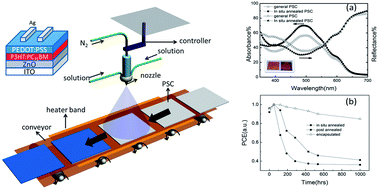
Efficient spray-coated inverted polymer solar cells (PSCs) based on a poly(3,4-ethylenedioxythiophene):poly(styrenesulfonate) (PEDOT:PSS) hole transport layer (HTL) are investigated by incorporating an in situ annealing treatment. Compared to conventional annealed devices, the in situ annealed PSCs exhibited a 25.5% and 47.7% enhancement in fill factor and power conversion efficiency (PCE) respectively, as well as about a two-fold improvement in the device lifetime. The performance enhancement was attributed to the improvement of the vertical phase separation of the PEDOT:PSS HTL and the reduction of the residual humidity of the HTL. This approach significantly enhances our understanding of the application of the PEDOT:PSS HTL in inverted PSCs, and illuminates the potential of spray coating for the sustainable commercial fabrication of PSCs with high PCEs.
1 Introduction
Polymer solar cells (PSCs) have attracted great attention as next-generation light harvesting devices, due to their light weight, mechanical flexibility, and tunable optical and electronic properties.1–4 Compared to conventional bi-layer structure devices, bulk-heterojunction (BHJ) PSCs exhibit the homogeneous contact of the donor (D)/acceptor (A) interface to facilitate a longer mean free path for excitons, which circumvents the long diffusion length and large Coulomb attraction of electron–hole pairs caused by the low dielectric constant (εr ≈ 2–4) of the organic semiconductor, and localizes the nature of the electronic state.5 In recent years, efforts on PSCs, including the development of novel organic materials, the optimization of device architectures and fabrication methods, have resulted in a power conversion efficiency (PCE) greater than 10% being reported.6–8 However, the downhill energy transfer of the charge carrier, and the aggregation and inhomogeneous mixing of the D/A blend may result in the trap states of excitons, leading to geminate and bimolecular recombination during the diffusion process.9 In this case, a buffer layer, acting as the hole transport layer (HTL) or electron transport layer (ETL), is indispensable to ensure that the charges can diffuse into the corresponding electrodes.10
Among the ETLs employed in PSCs, zinc oxide (ZnO) and titanium dioxide (TiO2) have been widely investigated,6,11 while poly(3,4-ethylenedioxythiophene):poly(styrenesulfonate) (PEDOT:PSS) is the most promising HTL of PSCs, due to its high work function, excellent conductivity and optical transparency.12,13 In addition, the aqueous dispersion of PEDOT/PSS makes it possible to realize high performance all-solution-processed PSCs.14 Despite the attraction of the PEDOT:PSS HTL in PSCs, the corrosive nature of PEDOT:PSS can compromise the device stability.15,16 The inverted structure in PSCs, a mainstay of research in the past few years, can effectively improve the device stability, since the electrode is protected by the ambient stable oxide.17 However, there are still several obstacles for the utilization of PEDOT:PSS as the HTL in inverted PSCs. Firstly, due to the different polarity of solvents between the organic film and the upper PEDOT:PSS HTL, the PEDOT:PSS HTL can not be easily deposited by the most widely used spin-coating method. Secondly, to obtain the high hole transport capability, the PEDOT:PSS HTL should be treated by post-thermal annealing (>100 °C).18,19 This would probably cause an interference of the active layers in the inverted PSCs, changing the aggregation and crystallization of the active layers, and leading to a short current density change.5,20 Additionally, the conventional annealing treatment breaks the continuity of the solution process, and redox reactions between the active layer and ambient oxygen/water during the long time annealing process is detrimental to the device's lifetime.21,22 The above issues hinder its potential in the sustainable commercial application of PSCs in large scale production. Hence, how to find a time-saving and energy-economical method for the deposition of a homogeneous PEDOT:PSS HTL without breaking the process continuity is still an unsolved fundamental question for the realization of all-solution-processed inverted PSCs with considerable stability.23–25
Emerging as a promising method, spray coating is independent of solvent polarity, since the sprayed droplets are transferred directly from the spray nozzle to the substrate.26–28 Furthermore, combining spray coating and an in situ annealing treatment could reduce the processing time and lower the annealing temperature.26 Therefore, it can not only ensure the homogeneous deposition of the PEDOT:PSS HTL, but also facilitate the spray coating to match the commercial fabrication of PSCs. In this work, uninterruptedle fabrication process of the PEDOT:PSS HTL for spray-coated inverted PSCs was introduced by in situ annealing.25 The influence of the in situ annealed PEDOT:PSS HTL on both inverted and conventional structure PSCs using a co-solvent system was investigated in detail. It will be seen that this approach significantly enhances our understanding of the application of PEDOT:PSS HTLs in inverted PSCs by combining spray coating and in situ annealing, and leads to an improvement of both the PCE and air stability.
2 Experimental
2.1 Fabrication section
The device fabrication apparatus is shown in Fig. 1. For the inverted structure PSCs, the device configuration is ITO/ZnO (40 nm)/poly(3-hexylthiophene) (P3HT):[6,6]-phenyl-C71-butyric acid methyl ester (PC71BM) (200 ± 15 nm)/PEDOT:PSS (30 nm)/Ag (100 nm). A heater band was used for the annealing process: post-annealing at 130 °C for 30 min and in situ annealing at various temperatures during the spray coating process. ITO-coated glass substrates with a sheet resistance of 10 Ω sq−1 were consecutively cleaned in ultrasonic baths containing detergent, acetone, deionized water and ethanol for 10 min each, and then dried by nitrogen blowing. Prior to film deposition, the substrate was treated by UV light for 10 min. The ZnO precursor was prepared by dissolving zinc acetate dihydrate (Zn(CH3COO)2·2H2O, Aldrich, 99.9%, 1 g) and ethanolamine (NH2CH2CH2OH, Aldrich, 99.5%, 0.28 g in 2-methoxyethanol (CH3OCH2CH2OH, Aldrich, 99.8%, 10 mL) under vigorous stirring for 12 h for the hydrolysis reaction in air. The 30 nm ZnO ETL was spin-cast from the precursor solution on top of the clean ITO–glass substrate, and then annealed at 200 °C for 1 h in air.6 Next, the active layer of the 1
:
1 mixture of P3HT (99.9%, Aldrich) and PC71BM (99.9%, Lumtec) was prepared in 1,2-dichlorobenzene (DCB) at a concentration of 4 mg mL−1, and then spray-coated at a rate of 0.30 mL min−1 at a height of 20 cm. The HTL solution composed of PEDOT:PSS (Baytron P AI4083))
:
deionized water (DIW)
:
isopropanol (IPA), with a ratio of 50
:
20
:
30 vol%, was spray-coated with the optimized parameters at a rate of 0.25 mL min−1 and at a height of 17 cm to the substrate. Throughout the whole spray coating process, the airbrush was powered by N2 gas at a high pressure of ∼60 psi to ensure a fine nebulization of the solution. The Ag cathode of about 100 nm was finally deposited at a rate of 10 Å s−1 under a pressure of 3 × 10⁻³ Pa under vacuum conditions.
 |
| | Fig. 1 Schematic diagram of the spray coating apparatus in this study. The devices were set on the transport tape, then the active layer P3HT:PC71BM was spray-coated at a rate of 0.30 mL min−1 at 20 cm height, followed by HTL spray coated at a rate of 0.25 ml min−1, at a height of 17 cm. The heater band under the transport tape was controlled to heat the substrate. All of the apparatus was stored in ambient conditions. | |
In contrast, the device configuration of conventional structure PSCs was ITO/PEDOT:PSS (30 nm)/P3HT:PC71BM (220 nm)/4,7-diphenyl-1,10-phenanthroline (Bphen) (5 nm)/Ag (100 nm). The PEDOT:PSS HTL solution and the P3HT:PC71BM active layer solution were spray-coated on the substrate with the above-mentioned parameters. The ultrathin cathode interfacial layer, Bphen (∼5 nm, 99%, Fluka), was thermally evaporated through OLED-V vacuum deposition equipment at a rate of 1 Å s−1 under a pressure of 3 × 10⁻⁴ Pa.29 Finally, the 100 nm Ag cathode was deposited under the same conditions.
2.2 Measurement method
Current density–voltage (J–V) curves in the dark and under illumination were measured with a Keithley 4200 programmable voltage–current source. A xenon lamp (CHF-XM35, Beijing Trusttech) with an illumination power of 100 mW cm−2 was used as an illumination source.30 All of the measurements were performed in air. The thicknesses of the vacuum deposited films were in situ monitored using a quartz crystal oscillator. The thicknesses of the film obtained from the solution process were measured with a Dektak 150 stylus profiler. The absorption and reflection spectra were measured with a Shimadzu UV1700 system. The surface morphologies of the PEDOT:PSS films were monitored by atomic force microscopy (AFM) (MFP-3D-BIO, Asylum Research). All of the measurements were performed in air under ambient conditions without device encapsulation.
3 Results and discussion
3.1 Optimizing the spray parameters
Fig. 1 shows a schematic of the apparatus for fabricating PSCs by continuous processing in this study. The film fabricated by spray coating can be affected by many factors including the spray coating deposition rate, substrate temperature and the solvent properties. The solvent experiences evaporation during the spray coating process, which is inversely proportional to the nebulization extent and the boiling point of the solution. The relatively dry film facilitates the crystallization or aggregation process of the hole transport unit, which would enhance the charge transport mobility to some extent.25 Therefore, the spray coating parameters should be scrupulously optimized before investigating the influence of in situ annealing on the PEDOT:PSS thin film.31
As shown in Fig. 2, with a suitable spray height about 17 cm, spray-coated films can avoid the aggregation caused by large-size wet drops (∼8 μm) with appropriate humidity.28 It is obvious through the microscopy images that the PEDOT:PSS domain aggregates in a relatively large size (about 16 μm) when the spray height is lower than 16 cm. In contrast, a higher height (over 20 cm) could result in a smooth film surface with many independent islands that limit the hole mobility of the HTL. Hence, a height of 18.5 cm between the nozzle and substrates is suitable for spraying the PEDOT:PSS solution at a rate of 0.3 mL min−1 to form a relatively smooth surface with fewer pin holes, the same as the surface of frosted glass.
 |
| | Fig. 2 Surface morphology of the PEDOT:PSS HTL under a ramped spray height. (a) and (d) are at spray heights of 20 and 21 cm, respectively. The height >20 cm could result in a relatively smooth film surface. (b) and (e) are at spray heights of 17 and 18 cm, respectively. The PEDOT:PSS domains aggregate in a relatively large size (∼8 μm) when the spray height is <16 cm. (c) and (f) are at 14 and 15 cm respectively. | |
The solvent properties directly determine the conductivity and chemical properties of the film.32 It is critical to modify the solvent properties in order to obtain the homogeneous PEDOT:PSS HTL. The hydrophilic PEDOT:PSS droplets deposited on the hydrophobic active layer tend to form a spherical cap shape rather than a thin wet layer, exhibiting a large contact angle. Adding a surfactant is one of several strategies to reduce the contact angle of the solution. Although the high surface tension of the solution could be significantly reduced, the surfactant may remain in the solid film to affect the electrical behavior of the device. Another strategy is the utilization of a co-solvent system. According to the Young equation,33 cos
θc = (γSV − γSL)/γ, where θc is the contact angle of the droplet, γ is its surface tension, and γSV and γSL represent the solid–vapor phase and the solid–liquid phase, respectively.
By introducing another solvent with a lower surface tension and a higher vapor pressure, the co-solvent could evaporate faster than the solo-solvent, leading to the solute breaking the boundary and forming the Marangoni flow. Isopropanol (IPA) is a good candidate as a solvent of PEDOT:PSS co-solvent systems, since it can not only improve the contact properties but also ensure the full coverage of the spray-coated film.34 However, the large cluster retraction can not be easily eliminated in such a co-solvent system by only reducing the surface tension.34 The low concentration of deionized water (DIW) in the co-solvent system is critical to limit the retraction of PEDOT:PSS and IPA. According to the previous work of Girotto et al.,28 we chose the co-solvent system IPA
:
DIW
:
(PEDOT:PSS) with ratio of 50
:
20
:
30 vol%. The PSCs based on the PEDOT:PSS HTL with and without the co-solvent system were fabricated, and the corresponding device performances are shown in Fig. 3a and Table 1. It can be observed that the fill factor (FF) of the device fabricated by using the co-solvent system increased significantly from 46.5% to 54.2%, which may be ascribed to the improvement of the contact properties between the active layer and the PEDOT:PSS HTL. Here, by introducing IPA of 50% volume content, the boiling point of the co-solvent system decreased from 100 to 80 °C, and the surface tension reduced from 2.5 m Nm−1 to about 0.8 m Nm−1.28 A series resistance (RS) of 2.0 Ω cm2 could also be obtained, compared to 11.96 Ω cm2 for the pure PEDOT:PSS dispersion.
 |
| | Fig. 3 Current density versus voltage (J–V) characteristics of the devices (ITO/ZnO(40 nm)/P3HT : PC71BM (200 ± 15 nm)/PEDOT:PSS (30 nm)/Ag (100 nm)): (a) comparison and (b) at various temperatures. | |
Table 1 Summary of the photovoltaic parameters of the device performance fabricated with different annealing treatments
| Temperature (°C) |
VOC (V) |
JSC (mA cm−2) |
FF (%) |
PCE (%) |
RS (ohm cm2) |
| Post-annealed 130 |
0.586 |
9.48 |
46.5 |
2.58 |
11.90 |
| In situ 50 |
0.557 |
8.19 |
52.4 |
2.39 |
4.89 |
| In situ 60 |
0.601 |
8.85 |
52.1 |
2.76 |
1.64 |
| In situ 70 |
0.566 |
10.8 |
54.7 |
3.33 |
1.71 |
| In situ 80 |
0.591 |
11.1 |
53.4 |
3.52 |
6.18 |
| In situ 90 |
0.584 |
9.54 |
52.9 |
2.95 |
5.85 |
| In situ 110 |
0.593 |
9.19 |
51.1 |
2.78 |
2.48 |
3.2 Influence of in situ annealing on the PEDOT:PSS HTL
3.2.1 Thermal mechanism of in situ annealing. To investigate the thermal mechanism of the in situ annealing process, we characterized the morphology of in situ annealed PEDOT:PSS solid film using AFM. The current density–voltage (J–V) curves revealing the device performance are shown in Fig. 3b. The morphologies of the PEDOT:PSS films show obvious discrepancies under different in situ annealing temperatures ranging from 50 to 110 °C, as depicted in Fig. 4a–d. In the PEDOT:PSS composite, PEDOT is hydrophobic and conductive,35 and the way in which PEDOT:PSS is formed directly determines the conductivity of the film. At 50 °C, the PEDOT:PSS film exhibits a smooth surface with a RMS of 1.0 nm, with more narrow strips and less phase separation of PEDOT:PSS, as shown in Fig. 4a. As the temperature increased to 70 °C, the inner PSS chains, which were used as a charge-balancing dopant during PEDOT:PSS polymerization, moved to the surface of the film with the evaporated solvent, and presented as narrower strips.36,37 In this case, more PSS chains gather at the surface, resulting in the formation of larger grains, enhancing the hole transporting capability in the PEDOT:PSS HTL. Hence, as shown in Fig. 4b, the device JSC was enhanced significantly, from 8.85 to 10.8 mA cm−2. We ascribed the JSC enhancement to the spontaneous formation of a highly enriched PSS layer on the top surface and the better 3-dimensional structure rearrangement in the PEDOT:PSS solid film, which represented the formation of a noticeable vertical phase separation between the PSS and PEDOT chains.38 The noticeable spontaneous formation of a highly enriched PSS layer on the top surface corresponds to better dc conductivity, as reported by Nardes et al.39 The rising trend in JSC did not stop until the in situ annealing temperature was higher than 80 °C. From 50 to 80 °C, the JSC improved by 35% from 8.19 to 11.1 mA cm−2, due to the optimized phase separation and suitable grain size. Hence, it provides a better conductive pathway for hole transporting from P3HT to the anode without being trapped or recombined in the HTL.13 The rising trend in JSC also made a contribution to the PCE improvement, from 2.39% at 50 °C to 3.52% at 80 °C.
 |
| | Fig. 4 AFM height images of the spray-coated PEDOT:PSS layer with in situ annealing temperatures of (a) 50 °C, (b) 70 °C, (c) 90 °C and (d) 110 °C. As a comparison to the in situ annealing, the post-annealed (130 °C, 30 min) PEDOT:PSS layer is shown in (e). | |
However, a higher in situ annealing temperature (>80 °C) could aggravate the evaporation rate of the solution, leading to a larger RMS of 2.2 nm. The rougher HTL film probably introduces some defects at the HTL/active layer interface, which would deteriorate the device FF and limit the PCE. The improved RMS of the film indicated that the contact area of the better-oriented PEDOT-rich grains to the active layer became larger, resulting in the increased conductivity by enhancing the conducting pathways for charge carriers.40 When the in situ annealing temperature was further increased above 90 °C, the larger grain size caused a rougher film surface (RMS = 6.0 nm), indicating that the PSS chains completely separated from the PEDOT segment.41,42 Decomposing the conductive pathway for hole transportation led to a decrease of both the JSC and FF, and also resulted in a decline of the PCE from 3.52% to 2.95%.
To further illuminate the effect of in situ annealing on the PEDOT:PSS HTL, we compared the morphology of the in situ annealed HTL with its post-annealed counterpart (130 °C, 30 min), and the result is shown in Fig. 4e. It can be seen that the morphology of in situ annealed PEDOT:PSS is similar to that of the long-time post-annealed solid film. Compared to the post-annealed device, the in situ annealed film exhibited a greatly improved FF, above 50% (as the dust in ambient air will inevitably affect the device during the spray coating process, the FF of these serial devices is still lower than the device fabricated in a nitrogen box, which is about 70%). The post-annealed PEDOT:PSS device exhibited a higher RS of 11.9 Ω cm2 and a larger RMS of 3.6 nm, which may be the major limitation of the device performance, as shown in Table 1. The conductivity of PEDOT:PSS was increased with the rise of the in situ annealing temperature, which is represented by the square resistance (RSq) in Fig. 5a. The highest performance was obtained at 80 °C in situ annealing, due to the contribution of the optimized phase separation, appropriate roughness and high conductivity of the PEDOT:PSS HTL.
 |
| | Fig. 5 (a) Parameters of the PEDOT:PSS HTL. Square resistance (RSq) decreased with the increase of the in situ temperature, which is opposite to the trend of RMS. (b) J–V characteristics of the devices with different drying times. Inset: EQE of the in situ annealed PSC at 80 °C, dried for 4 min. The drying time could determine the phase separation and morphology of PEDOT:PSS which affects the charge transport and conductivity properties of the HTL. The FF increased from 54% to 59% at the drying time of 4 min and the VOC improved from 0.56 to 0.61 V on raising the drying time from 0 to 6 min. | |
3.2.2 Drying time of in situ annealing. It is well known that the drying time and the amount of polar solvent in PEDOT:PSS films are crucial to its conductivity,38 as the phase separation and morphology changes of PEDOT:PSS films are observed with polar solvents and water evaporation. These will also affect the charge transportation and conductivity properties of the HTL.43–45 To further optimize the device performance, we fabricated a series of devices with a variety of drying times at the optimized in situ annealing temperature of 80 °C. The performance and detailed parameters of the devices are shown in Fig. 5b and Table 2, respectively.
Table 2 Detailed parameters of the in situ annealed PSCs with various drying times
| Drying time (min) |
VOC (V) |
JSC (mA cm−2) |
FF (%) |
PCE (%) |
RS (ohm cm2) |
RP (ohm cm2) |
| 0 |
0.563 |
10.0 |
54.0 |
3.05 |
2.11 |
253.5 |
| 2 |
0.573 |
10.4 |
56.6 |
3.37 |
3.78 |
289.1 |
| 4 |
0.592 |
10.9 |
59.0 |
3.81 |
0.79 |
317.0 |
| 6 |
0.607 |
10.6 |
58.4 |
3.74 |
1.16 |
301.4 |
| 8 |
0.603 |
9.6 |
55.5 |
3.23 |
1.69 |
289.4 |
| 10 |
0.582 |
9.7 |
53.3 |
3.01 |
4.22 |
330.4 |
It can be observed that when the drying time increased, the FF is significantly improved, increasing from 54% to 59% as the drying time is varied from 0 to 4 min. We attributed this improvement in FF to the lower interaction between the PEDOT core and excess PSS.46 If the solvent had completely evaporated during the process of droplet sprayed from the nozzle to the substrate, there would not be enough space for the dynamic transportation of both PEDOT and PSS, which would result in a limitation of the FF. Meanwhile, a suitable amount of residual solvent would enable the PSS to easily migrate in a thermodynamically favorable direction and pave the way for hole transportation, which is also consistent with the decrease in the series resistance. However, the longer solvent drying time leads to a wetter film, and if the film is too wet, it may cause the excess aggregation of PEDOT chains, which may be detrimental to the conductivity of the film and increase the film’s RMS, resulting in the decrease of both the JSC and FF. In addition to the change in JSC and FF, the VOC increased and then decreased with the rising drying time. The work function could be systematically tuned with the solvent drying time.47 When the solvent drying time was controlled at 4–6 min, the excess PSS was able to migrate to the top of the film, leading to the filled state density decreasing near the Fermi level. By increasing the work function of the PEDOT:PSS HTL, the VOC was enhanced from 0.56 to 0.61 V as the drying time was raised from 0 to 6 min. The variety in VOC also demonstrated better phase separation, and higher dc conductivity of the PEDOT:PSS solid film could be obtained by introducing in situ annealing.48
3.3 In situ annealed all-solution-processed inverted PSCs
Incorporating in situ annealing with a spray coating system, all-solution-processed PSCs based on the PEDOT:PSS HTL can be fabricated continuously and efficiently. Compared to the PSCs by the conventional fabrication process, in situ annealed devices (including an active layer and HTL) exhibit a much higher current density. Through absorption spectra measurements, we attributed this relatively high current density of the in situ annealed PSC to the better absorption and lower reflection of the active layer, as shown in Fig. 6a. In situ annealing-treated P3HT:PC71BM exhibits stronger absorption at 500 nm, which may result from the aggregation effect of PC71BM and phase separation between the donor and acceptor.49 As the solvent evaporates as the droplet reaches the substrate, the solute disperses into the wet film and then aggregates at a high rate, leading to increased crystallization of the solute and a rougher film surface compared to the film deposited by other deposition processes. Incident light would be more properly trapped in the film rather than vertical reflection or travelling through the device, which is consistent with the lower reflection of the in situ annealed P3HT
:
PCBM film from 400 nm to 600 nm. More light would be dispersed in these solid films. Another possible reason is the reduction in geminate recombination losses,50 as shown in the inset of Fig. 5b. The external quantum efficiency (EQE) of the in situ annealed inverted PSC reaches a high level of about 60% from 450 nm to 650 nm. In the P3HT
:
PC71BM system, nebulized droplets could limit the donor domain size under 20–30 nm in the solid film, which is beneficial for charge transportation and the dissociation of the CT-state into free charges.
 |
| | Fig. 6 UV-vis absorption and reflection spectra of the in situ annealed P3HT:PCBM film compared to the general post-annealed film. Inset: image of the in situ annealed P3HT:PCBM film (left) and the post-annealed film (right). (b) Plot of the degradation rates of the inverted structure PCE. The in situ annealed device exhibits a more stable device performance with a lifetime (T50) of about 400 h, compared to 200 h for the post-annealed device. If the in situ annealed device was protected by encapsulation, the lifetime could be significantly increased (T80 > 1000 h). | |
3.4 Lifetime study
To disclose the air stability of the in situ annealed PSCs, we undertook shelf life studies by leaving modules in the dark room and periodically measuring the IV curves under ambient conditions. Fig. 6b shows the plot of the degradation rates of the PCE devices. To examine the influence of humidity on the device performance, the devices were kept under ambient conditions (60% humidity) without any protection by encapsulation. It has been reported that the degradation of conventional structure devices with the PEDOT:PSS HTL is highly dependent on humidity.51,52 Nevertheless, our inverted PSCs fabricated by in situ annealing were not strongly affected by the humidity: the device PCE remained at a high level for the first 200 h in this study. This was mainly because the in situ annealing could not only curtail the thermal annealing process (<2 min) that prevents the long-time photochemical reaction with P3HT and oxygen, but also decreases the residual humidity in the HTL. The low annealing temperature of in situ annealing circumvents the thermal degradation of PEDOT:PSS, resulting in a device lifetime (T80) of about 180 h, even better than that of post-annealed device (about 100 h).16 The lifetime (T50) of the in situ annealed device is about 420 h, which is two-fold that of the post-annealed device.15 The decrease after 400 h is mainly due to the decay of VOC, which may be affected by the redox reaction in the active layer.53–55 If the devices were protected by encapsulation, or the fabrication process was carried out under conditions with less dust and lower humidity, the stability of the PSCs could be further improved; the lifetime of the in situ annealed device (T80) was more than 1000 h by UV curing encapsulation, as shown in Fig. 6b.
3.5 Commercial potential of in situ annealing
In addition to the lifetime improvement, in situ annealing also makes a contribution to the device fabrication efficiency. At present, although the R2R technology exhibits the greatest potential for the large scale fabrication of PSCs, in terms of the recrystallization of organic materials at high temperature, the PCEs of the devices is still limited.19,24 Although introducing a heater band in the R2R system could solve the annealing problem, long-time independent post-annealing breaks the continuity of the deposition process.56 In contrast, in situ annealing is a promising alternative technique, which could be combined with the mobility of spray coating without limiting the production efficiency and breaking the process continuity. In addition, the morphology of organic films is able to be further modified by optimizing the in situ annealing parameters. Moreover, taking the applicability into consideration, in situ annealing could not only reduce the time and cost for spray coating to scrutinize novel materials with low solubility (<3 mg mL−1), but also allow those materials with low decomposition temperatures to be applied in diversiform structures.
4 Conclusion
In conclusion, in situ annealing treatment was introduced to modify the spray-coated PEDOT:PSS HTL for solution-processed inverted PSCs. It was observed that through incorporating in situ annealing, the vertical phase separation and interconnection in the PEDOT:PSS HTL were improved. Compared to conventional annealed PSCs, the in situ annealed inverted PSCs exhibited a 25.5% and 47.7% enhancement in FF and PCE, respectively. In addition, the lifetime of such PSCs was also improved by a factor of 2 due to the decreased residual humidity in the in situ annealed PEDOT:PSS HTL. Our study demonstrates a feasible approach for cost-effective, continuous process, large scale and sustainable commercial application of all-solution-processed PSCs.
Acknowledgements
This work was supported by the National Science Foundation of China (NSFC) (grant no. 61177032), the Foundation for Innovative Research Groups of the NSFC (grant no.61021061), the Fundamental Research Funds for the Central Universities (grant no. ZYGX2010Z004), and SRF for ROCS, SEM (grant no. GGRYJJ08-05).
References
- X. Guo, N. Zhou, S. J. Lou, J. Smith, D. B. Tice, J. W. Hennek, R. P. Ortiz, J. T. L. Navarrete, S. Li, J. Strzalka, L. X. Chen, R. P. H. Chang, A. Facchetti and T. J. Marks, Nat. Photonics, 2013, 7, 825 CrossRef CAS.
- W. Zhou, Z.-G. Zhang, L. Ma, Y. Li and X. Zhan, Sol. Energy Mater. Sol. Cells, 2013, 112, 13 CrossRef CAS PubMed.
- Y. Liu, T. T. Larsen-Olsen, X. Zhao, B. Andreasen, R. R. Sondergaard, M. Helgesen, K. Norman, M. Jorgensen, F. C. Krebs and X. Zhan, Sol. Energy Mater. Sol. Cells, 2013, 112, 157 CrossRef CAS PubMed.
- J. Huang, Y. Qi, H. Wang and J. Yu, Appl. Phys. Lett., 2013, 102, 183302 CrossRef PubMed.
- Y. Liu, X. Wang, F. Wang, J. Zhou, G. Long, J. Tian, J. You, Y. Yang and Y. Chen, Adv. Energy Mater., 2011, 1, 771 CrossRef CAS PubMed.
- M. A. Green, K. Emery, Y. Hishikawa, W. Warta and E. D. Dunlop, Prog. Photovoltaics, 2012, 20, 12 Search PubMed.
- G. Li, C.-W. Chu, V. Shrotriya, J. Huang and Y. Yang, Appl. Phys. Lett., 2006, 88, 253503 CrossRef PubMed.
- T. M. Clarke and J. R. Durrant, Chem. Rev., 2010, 110, 6736 CrossRef CAS PubMed.
- E. R. Bitter, R. J. G. Santos and S. J. Karabunarliev, J. Chem. Phys., 2005, 122, 214719 CrossRef PubMed.
- N. Wang, J. Yu, Y. Zang, J. Huang and Y. Jiang, Sol. Energy Mater. Sol. Cells, 2010, 94, 263 CrossRef CAS PubMed.
- T. Stubhan, N. Li, N. A. Luechinger, S. C. Halim, G. J. Matt and C. J. Brabec, Adv. Energy Mater., 2012, 2, 1433 CrossRef CAS PubMed.
- W. Jonas, H. Sun, P. Claudia, H. C. Hesse and S.-M. Lukas, Sol. Energy Mater. Sol. Cells, 2010, 94, 2371 CrossRef PubMed.
- J. S. Yang, S. H. Oh, D. L. Kim, S. J. Kim and H. J. Kim, ACS Appl. Mater. Interfaces, 2012, 4, 5394 CAS.
- H. Kim, S. Nam, H. Lee, S. Woo, C.-S. Ha, M. Ree and Y. Kim, J. Phys. Chem. B, 2011, 115, 13502 CrossRef CAS PubMed.
- E. Vitoratos, S. Sakkopoulos, E. Dalas, N. Paliatsas, D. Karageorgopoulos, F. Petraki, S. Kennou and S. A. Choulis, Org. Electron., 2009, 10, 61 CrossRef CAS PubMed.
- E. Voroshazi, B. Verreet, T. Aernouts and P. Heremans, Sol. Energy Mater. Sol. Cells, 2011, 95, 1303 CrossRef CAS PubMed.
- Z. He, C. Zhong, X. Huang, W.-Y. Wong, H. Wu, L. Chen, S. Sun and Y. Cao, Adv. Mater., 2011, 23, 4636 CrossRef CAS PubMed.
- T. Aemouts, T. Aleksandrov, C. Girroto, J. Geoe and J. Poortmans, Appl. Phys. Lett., 2008, 92, 003306 Search PubMed.
- L.-M. Chen, Z. Hong, W. L. Kwan, C.-H. Lu, Y.-F. Lai, B. Lei, C.-P. Liu and Y. Yang, ACS Nano, 2010, 4, 4744 CrossRef CAS PubMed.
- N. Zhou, H. Lin, S. J. Lou, X. Yu, P. Guo, E. F. Manley, S. Loser, P. Hartnett, H. Huang, M. R. Wasielewski, L. X. Chen, R. P. H. Chang, A. Facchetti and T. J. Marks, Adv. Energy Mater., 2013, 4, 1098 Search PubMed.
- F. C. Krebs, Sol. Energy Mater. Sol. Cells, 2009, 93, 394 CrossRef CAS PubMed.
- M. Jorgensen, K. Norrman, S. A. Gevorgyan, T. Tromholt, B. Andreasen and F. C. Krebs, Adv. Mater., 2012, 24, 580 CrossRef PubMed.
- S. K. Hau, H.-L. Yip, K. Leong and A. K.-Y. Jen, Org. Electron., 2009, 10, 719 CrossRef CAS PubMed.
- F. C. Krebs, Sol. Energy Mater. Sol. Cells, 2009, 93, 484 CrossRef CAS PubMed.
- F. C. Krebs, Sol. Energy Mater. Sol. Cells, 2009, 93, 465 CrossRef CAS PubMed.
- Y. Zheng, R. Wu, W. Shi, Z. Guan and J. Yu, Sol. Energy Mater. Sol. Cells, 2013, 111, 200 CrossRef CAS PubMed.
- T. Aemouts, T. Aleksandrov, C. Girroto, J. Geoe and J. Poortmans, Appl. Phys. Lett., 2008, 92, 003306 Search PubMed.
- C. Girotto, D. Moia, B. P. Rand and P. Heremans, Adv. Funct. Mater., 2011, 21, 64 CrossRef CAS PubMed.
- J. Yu, N. Wang, Y. Zang and Y. Jiang, Sol. Energy Mater. Sol. Cells, 2011, 95, 664 CrossRef CAS PubMed.
- N. Wang, J. Yu, Y. Zheng, Z. Guan and Y. Jiang, J. Phys. Chem. C, 2012, 116, 5887 CAS.
- B. K. Yu, D. Vak, J. Jo, S. I. Na, S. S. Kim, M. K. Kim and D. Y. Kim, IEEE J. Sel. Top. Quantum Electron., 2010, 16, 1838 CrossRef CAS.
- W. Shi, J. Yu, W. Huang, X. Yu and Y. Zheng, Appl. Phys. Lett., 2013, 102, 111607 CrossRef PubMed.
- J. S. Rowlinson and B. Widom, Molecular Theory of Capillarity, Clarendon, Oxford, 1982 Search PubMed.
- C. Liu, E. Bonaccurso and H.-J. Butt, Phys. Chem. Chem. Phys., 2008, 10, 7150 RSC.
- D. R. Lide, in CRC Handbook of Chemistry and Physics, CRC press, 85th edn, 2004– 2005 Search PubMed.
- U. Lang, E. Muller, N. Naujoks and J. Dual, Adv. Funct. Mater., 2009, 19, 1215 CrossRef CAS PubMed.
- S. Timpanaro, M. Kemerink, F. J. Touwslager, M. M. D. Kok and S. Schrader, Chem. Phys. Lett., 2004, 394, 339 CrossRef CAS PubMed.
- J.-S. Yeo, J.-M. Yun, D.-Y. Kim, S. Park, S.-S. Kim, M.-H. Yoon, T.-W. Kim and S.-I. Na, ACS Appl. Mater. Interfaces, 2012, 4, 2551 CAS.
- A. M. Nardes, M. Kemerink, R. A. J. Janssen, J. A. M. Bastiaansen, N. M. M. Kiggen, B. M. W. Langeveld, A. J. J. M. van Breemen and M. M. de Kok, Adv. Mater., 2007, 19, 1196 CrossRef CAS PubMed.
- Y. H. Kim, S. Christoph, L. M. Michael, M. Christian, M.-M. Lars and L. Karl, Adv. Funct. Mater., 2011, 21, 1076 CrossRef CAS PubMed.
- J. Quyang, Q. Xu, C.-W. Chu, Y. Yang, G. Li and J. Shinar, J. Polym. Sci., Part A: Polym. Chem., 2004, 45, 8443 Search PubMed.
- J. Quyang, C.-W. Chu, F.-C. Chen, Q. Xu and Y. Yang, Adv. Funct. Mater., 2005, 15, 203 CrossRef PubMed.
- A. M. Narders, R. A. J. Janssen and M. A. Kemerin, Adv. Funct. Mater., 2008, 18, 865 CrossRef PubMed.
- S.-I. Na, G. Wang, S.-S. Kim, T.-W. Kim, S.-H. Oh, B.-K. Yu, T. Lee and D.-Y. Kim, J. Mater. Chem., 2009, 19, 9045 RSC.
- X. Crispin, F. L. E. Jakobsson, A. Crispin, P. C. M. Grim, P. Andersson, A. Volodin, C. Van Haesendonck, M. Van der Auweraer, W. R. Salaneck and M. Berggren, Chem. Mater., 2006, 18, 4354 CrossRef CAS.
- J. Huang, P. F. Miller, J. S. Wilson, A. J. de Mello, J. C. de Mello and D. D. C. Bradley, Adv. Funct. Mater., 2005, 15, 290 CrossRef CAS PubMed.
- T.-W. Lee and Y. Chung, Adv. Funct. Mater., 2008, 18, 2246 CrossRef CAS PubMed.
- H. Ma, H.-L. Yip, F. Huang and A. K.-Y. Jen, Adv. Funct. Mater., 2010, 20, 1371 CrossRef CAS PubMed.
- S.-L. Na, T.-S. Kim, S.-H. Oh, J. Kim, S.-S. Kim and D.-Y. Kim, Appl. Phys. Lett., 2010, 97, 223305 CrossRef PubMed.
- T. M. Clarke, A. M. Ballantyne, J. Nelson, D. D. C. Bradley and J. R. Durrant, Adv. Funct. Mater., 2008, 18, 4029 CrossRef CAS PubMed.
- E. Voroshazi, B. Verreet, A. Buri, R. Muller, D. Di Nuzzo and P. Heremans, Org. Electron., 2011, 12, 736 CrossRef CAS PubMed.
- K. Norrman, M. V. Madse, S. A. Gevorgyan and F. C. Krebs, J. Am. Chem. Soc., 2010, 132, 16883 CrossRef CAS PubMed.
- J. Schafferhans, A. Bamann, A. Wagenpfahl, C. Deibel and V. Dyakonov, Org. Electron., 2010, 11, 1693 CrossRef CAS PubMed.
- A. Aguirre, S. C. J. Meskers, R. A. J. Janssen and H.-J. Egelhaaf, Org. Electron., 2011, 12, 1657 CrossRef CAS PubMed.
- A. Seemann, T. Sauermann, C. Lungenschmied, O. Armbruster, S. Bauer, H.-J. Egelhaaf and J. Hauch, Sol. Energy, 2011, 85, 1238 CrossRef CAS PubMed.
- S. R. Dupont, M. Oliver, F. C. Krebs and R. H. Dauskardt, Sol. Energy Mater. Sol. Cells, 2012, 97, 171 CrossRef CAS PubMed.
|
| This journal is © The Royal Society of Chemistry 2014 |
Click here to see how this site uses Cookies. View our privacy policy here.