Tin sulfide (SnS) nanorods: structural, optical and lithium storage property study†
Alok M. Tripathi and
Sagar Mitra*
Electrochemical Energy laboratory, Indian Institute of Technology Bombay, Mumbai, 400076, India. E-mail: sagar.mitra@iitb.ac.in; Fax: +91-22-2576-4890; Tel: +91-22-2576-7890
First published on 20th December 2013
Abstract
Tin mono-sulfide (SnS) nanorods (NRs) have been successfully synthesized through a solvothermal process using hydrated tin(II) chloride and sodium sulfide as precursors and N,N-dimethyl formamide (DMF) as solvent. The Reitveld refined powder X-ray diffraction (PXRD), Raman and 119Sn solid-state NMR experiments have confirmed the presence of a SnS phase with Pnma space group and a SnS2 phase with P![[3 with combining macron]](https://www.rsc.org/images/entities/char_0033_0304.gif) m1 space group as a minor impurity. HRTEM and HRSEM studies have confirmed the nanoparticle shape as nanorods (NRs). The growth of the NRs has been explained from the observation that by increasing the solvothermal temperature, nanorods grow preferentially in the [100] direction. Optical properties of the SnS nanorods were measured and it was found that all NRs have an indirect band gap in the range of 1.10 eV to 1.2 eV. The electrochemical properties for lithium storage (half-cell configuration) have been tested against Li/Li+ using conventional polyvinylidene fluoride (PVDF) binder and an eco-friendly, low cost binder, carboxy methyl cellulose (CMC). After fifty cycles of charge–discharge, the CMC binder electrode shows a superior electrochemical charge storage property of 591 mA h g−1 compared with 385 mA h g−1 for the PVDF binder electrode, at 160 mA g−1 current rate. At a high current rate of 350 mA g−1, the SnS NRs with the CMC binder shows a discharge capacity of 565 mA h g−1 after 50 cycles, therefore exhibiting excellent properties for a lithium battery anode as it can maintain a high capacity and coulombic efficiency continuously for 50 cycles.
m1 space group as a minor impurity. HRTEM and HRSEM studies have confirmed the nanoparticle shape as nanorods (NRs). The growth of the NRs has been explained from the observation that by increasing the solvothermal temperature, nanorods grow preferentially in the [100] direction. Optical properties of the SnS nanorods were measured and it was found that all NRs have an indirect band gap in the range of 1.10 eV to 1.2 eV. The electrochemical properties for lithium storage (half-cell configuration) have been tested against Li/Li+ using conventional polyvinylidene fluoride (PVDF) binder and an eco-friendly, low cost binder, carboxy methyl cellulose (CMC). After fifty cycles of charge–discharge, the CMC binder electrode shows a superior electrochemical charge storage property of 591 mA h g−1 compared with 385 mA h g−1 for the PVDF binder electrode, at 160 mA g−1 current rate. At a high current rate of 350 mA g−1, the SnS NRs with the CMC binder shows a discharge capacity of 565 mA h g−1 after 50 cycles, therefore exhibiting excellent properties for a lithium battery anode as it can maintain a high capacity and coulombic efficiency continuously for 50 cycles.
1. Introduction
Energy materials with low-dimensional structures offer more benefits compared with other energy materials because of their high surface reactivity and extraordinary access to the material–material interface. In particular, one dimensional (1D) materials have shown excellent behaviour in their optical, electrical and magnetic properties in comparison with their bulk counterparts.1–6 In a similar way, earth-abundant IV–VI metal chalcogenides-based semiconductors are also known for their narrow band gap, and are of great interest in the fields of optics, electronics and optoelectronics.7–11The search for new negative electrode materials in lithium ion batteries began with metallic alloys, metal oxides, metal nitrides and metal phosphides etc.12–19 However, beyond basic binary lithium alloys, a large amount of attention has been given to the conversion of metal oxides, recently.16,19 The conversion of metal oxides consists of a metal which either can or cannot alloy with lithium. However, the former case where the metal can alloy with lithium in the first discharge cycle and will continue to show an alloying–dealloying reaction upon cycling is our current interest.
The search for an alloy–dealloy-based anode has recently led to investigations into areas that have been largely ignored, mainly non-traditional MX materials, where M is a metal and X can be S, P or N. There is a scarcity of current literature in this area, but the electrochemistry of such materials is quite rich and interesting. One such example is metal sulfide-based materials that have unique properties like abundance, high electrical conductivity, lower expense, and high catalytic activity, making them popular in the fields of micro and nano-electronics.20–25 Among them, tin sulfide in particular can be found in several phases like SnS, SnS2, Sn2S3, Sn3S4 and Sn4S5 and is attractive for lithium-ion storage applications.26–31 Most of the reports show the use of the SnS2 phase as it is an important mid-band gap semiconductor having a wide range of applications7,32,33 including promising electrochemical activity as a lithium battery anode.27–31 However, a tin(II) monosulfide (SnS) based nanomaterial as a lithium-ion battery anode with preferred electrochemical activity and stability is sporadic in the literature.34–39
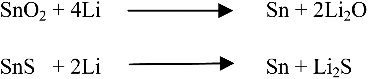
Recently, tin chalcogenides have shown better electrochemical properties against Li/Li+ and Na/Na+ electrodes because they can reversibly alloy and dealloy with lithium and sodium.34,40 Tin has a rich lithium electrochemistry because it can accommodate 4.4 moles of lithium per mole of tin atoms in the reduction process, making it superior to traditionally used graphite anodes. Synthesis of metallic tin is difficult because it has a high tendency to oxidize in any practical experimental conditions. Therefore, the most preferred compounds of tin are tin oxide (SnO2) or tin sulfide/tin disulfide (SnS/SnS2). Although the SnO2 and SnS have the same theoretical capacity (∼782 mA h g−1) against Li/Li+, SnS dominates over SnO2 because of less energy loss after the first cycle. The loss in energy in the first discharge cycle occurs due to the irreversible formation of Li2S or Li2O.19,27 Theoretically, this is clear from the possible chemical reactions shown in Scheme 1. The loss of lithium in the first discharge cycle of electrochemical lithiation to SnS is two times lower than that of SnO2, i.e. the loss of Li in the electrochemical reaction as an irreversible by-product (Li2O and Li2S) is two moles per mole of tin atoms in the SnO2 case compared with one mole per mole of SnS.
 | ||
| Scheme 1 Reaction of lithium with tin chalcogenide. | ||
This unique property arises because Sn can exist in the +II state as well as the +IV oxidation state in sulfides, while in oxides it exists mostly in the +IV state. Moreover, electrode materials used in battery applications must have better ionic diffusivity and electronic conductivity. The electronic conductivity of the material is governed by its band gap. The band gap of a material is also responsible for the interfacial electronic transfer in the electrode during lithiation and delithiation processes. Recently, the role of band gap engineering has been studied with germanium nanowires used as the anode in lithium ion batteries.41
In short, we would like to prepare a low dimensional phase of pure SnS and use it as an efficient lithium battery anode. We have successfully prepared NRs of a SnS phase, with a minor impurity phase of SnS2, using a solvothermal process. In most of the literature based on tin sulfide, the phase identification is doubtful or incomplete. Therefore, here we have made an effort to resolve the phase identification problem with the help of extensive experimental support. Impact of the solvothermal temperature on the NRs’ morphology and its impact on the optical band gap energy have also been studied here. As-prepared SnS NRs at 160 °C have been cycled against Li metal in a half cell configuration. The major concern in alloying-type reactions is the volume expansion, which leads to a loss in capacity and stability of the cell. For the stability concerns, the SnS compatibility has been tested with two different binders, CMC and PVDF, which have different elasticity. As a result, the SnS–CMC anode showed excellent electrochemical activity and stability for fifty charge–discharge cycles compared with the SnS–PVDF electrode.
2. Experimental section
2.1 Synthesis of SnS nanorods
NRs of SnS have been synthesized by mixing SnCl2·2H2O (Merck, India) and Na2S (Fisher Scientific) with a molar ratio of 1![[thin space (1/6-em)]](https://www.rsc.org/images/entities/char_2009.gif) :2 in 50 ml of N,N-dimethylformamide (DMF, Merck, India). The mixture was stored in a solvothermal bomb at a fixed temperature for 48 h. Temperatures of 140 °C, 160 °C, 180 °C and 200 °C were imposed for the solvothermal synthesis. The solvothermal bomb (100 ml) has a steel body with a thin Teflon liner and has dimensions of 5.5 cm × 4.3 cm × 3.4 mm (height × diameter × thickness). After completion of the reaction, the sample was washed with DI (deionized) water and acetone repeatedly. Drying of the washed sample was done under vacuum at 50 °C for 6 h and the as-prepared material was used for further characterization.
:2 in 50 ml of N,N-dimethylformamide (DMF, Merck, India). The mixture was stored in a solvothermal bomb at a fixed temperature for 48 h. Temperatures of 140 °C, 160 °C, 180 °C and 200 °C were imposed for the solvothermal synthesis. The solvothermal bomb (100 ml) has a steel body with a thin Teflon liner and has dimensions of 5.5 cm × 4.3 cm × 3.4 mm (height × diameter × thickness). After completion of the reaction, the sample was washed with DI (deionized) water and acetone repeatedly. Drying of the washed sample was done under vacuum at 50 °C for 6 h and the as-prepared material was used for further characterization.
2.2 Material characterization
Dried powder of the SnS (nanrods) was first characterized in a Rigaku Ultima IV diffractometer with scan step of 0.02° in the two theta (2θ) range of 05–70°. FullProf was used to do the Reitveld refinement of the powder diffraction data, in order to obtain qualitative crystallographic information and quantitative phase composition of the synthesized material.42 Raman spectroscopy was used to study the vibrational modes of the Sn–S bond with a Ramnor HG-2S Spectrometer, HORIBA Jobin Yvon, France, with an attached Quanta Laser system. Vacuum dried powder samples were used to obtain the Raman spectra with a laser of 514.4 nm wavelength and power of 10 mW. The acquisition time was 120 s and 20× magnification was used. Solid-state 119Sn-NMR spectra were recorded at room temperature (24–25 °C) with a Mercury Plus 300 MHz NMR Spectrometer, Varian, USA, fitted with a magic angle spin (MAS) facility, at an operating frequency of 200 MHz. The pulse width was 4 μs and the spinning frequency was 3 kHz with a zirconia rotor used in the present case. The delay time in successive pulses was 30 s and the number of scans was 1780. The reference used for the 119Sn-NMR spectroscopy was tetraphenyl tin(IV) having a reference shift at −128.15 ppm and the spectra was processed by GSim software.43 High resolution imaging of electron diffraction on the SnS sample (nanorods) was performed at 200 kV with FEG-TEM JEOL F-2100 and JEOL JSM-7600F models. X-ray photoelectron spectra were obtained with an XPS MULTILAB from Thermo VG Scientific, using Mg Kα X-rays and 100 W power with a vacuum level of <1.5 × 10⁻⁷ Pa in a calibration chamber. The diffuse reflectance test of the material was performed with a PerkinElmer Lambda 900 UV/Vis/NIR in the scan range of 250 nm to 2000 nm with a data acquisition interval of 1 nm and slit width of 2 nm.2.3 Electrochemical characterization
For electrochemical characterization, the anodes were prepared by mixing 70 wt% of the active material with 20 wt% carbon (super C-65, Timical, Switzerland) and 10 wt% PVDF/CMC binders in NMP (N-methyl-2-pyrrollidone)/water solvent, respectively. A thin film of the electrode material was cast on a Cu-foil by making a slurry of all the constituents in the appropriate solvents. All electrode films were dried in a vacuum oven at 120 °C for 4 h for the PVDF binder film and 80 °C for 24 h for the CMC binder, prior to use. The dried film was cut into a circular disc to fabricate the cell in a Swagelok-type cell assembly. The active mass of material for both binders on the circular disc was approximately 0.34 mg cm−2. Lithium metal was used as the counter and reference electrode. The electrolyte LP-30 (Merck, Germany) was used to soak a Whatman GF/D borosilicate glass fiber and used as a separator. Electrochemical testing including cyclic voltammetry and charge–discharge measurements were carried out with a Biologic VMP3 instrument and an Arbin battery tester (BT-2000 model), respectively, in a potential window of 0.01–1.2 V at 20 °C.3. Results and discussion
The solvothermal method is a simple one-step synthesis process, which is attractive to most researchers attempting to prepare 1D and 2D inorganic materials.44,45 Synthesis of the current material was performed with a high boiling point solvent like N,N-dimethylformamide (DMF). The possible reaction for SnS preparation is shown in Scheme 2. | ||
| Scheme 2 Chemical reaction scheme of SnS nanoparticle synthesis. | ||
At the end of the reaction, a black-brown precipitate was obtained, which was characterized further by the powder X-ray diffraction (PXRD) technique. The PXRD of the pristine material shows a perfect crystalline phase, which can be indexed to the orthorhombic system. Reitveld analysis of the diffraction pattern shows the presence of an orthorhombic SnS phase with Pnma space group and SnS2 as an impurity phase with Pm1 space group. Fig. 1(a) shows the fitted and experimental patterns for the powder X-ray diffraction with Bragg positions for both the phases. To obtain the amount of impurity, the X-ray diffraction pattern is further analyzed quantitatively, as shown in Fig. 1(a).
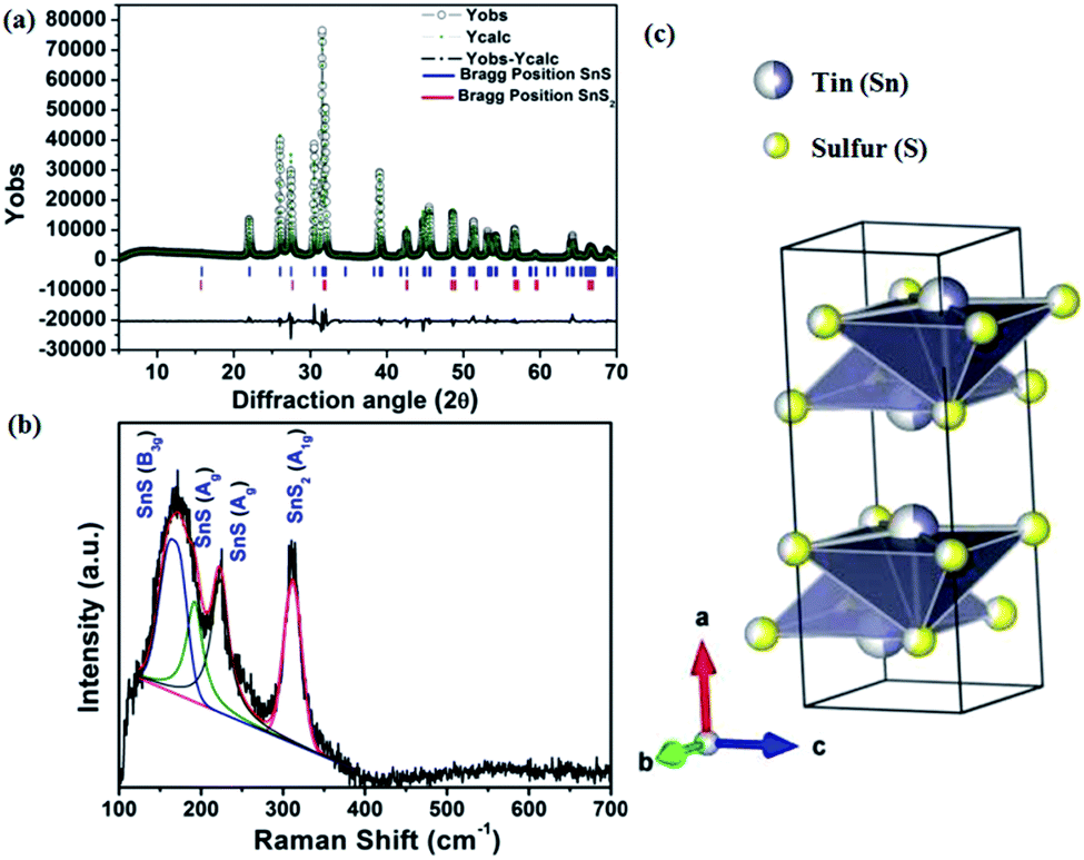 | ||
| Fig. 1 (a) Powder X-ray diffraction pattern of SnS (nanorod) and its Reitveld refinement (Rp = 10.2%, Rwp = 11.8%, Rexp = 2.38), (b) Raman spectrum of the SnS phase and (c) a visualization of the crystallographic arrangement of the SnS phase. | ||
The impurity of the SnS2 has been estimated using the Reitveld refinement of the powder XRD pattern and found to be ∼8%. The lattice parameters of orthorhombic SnS are found to be a = 11.19, b = 3.98, c = 4.20 and α = β = γ = 90°. The crystallographic arrangement of orthorhombic tin sulfide shows a layered arrangement of the SnS layers as shown in Fig. 1(c). This may be due to the inert lone pair effect of the tin that changes the normal NaCl structure and results in a separation of layers. To check for the presence of other phases in the as-synthesized SnS material, vibrational spectroscopy has been used in the present case. Raman spectroscopy is a typical technique used to identify the various allotropes of tin sulfide (like SnS, SnS2 and Sn2S3 etc.) by their distinct Raman shifts.46,47 Here, in the Raman spectrum shown in Fig. 1(b), the presence of four major shifts are observed after deconvolution of the original spectrum, and the positions are found to be at 311.77 cm−1, 222.69 cm−1, 191.89 cm−1 and 164.058 cm−1, corresponding to the A1g mode of SnS2, and the Ag, Ag and B3g modes of SnS, respectively.46,47 The peaks at 222.69 cm−1, 191.89 cm−1and 164.058 cm−1 confirm the presence of the SnS phase and the peak at 311.77 cm−1 confirms the presence of SnS2 as an impurity phase. Furthermore, the 119Sn solid-state CP-MASS NMR spectrum shown in Fig. 2(a) indicates a similar trend and shows that two phases co-exist in the sample, i.e. SnS and SnS2. The peak at a chemical shift of −128.25 ppm corresponds to tetraphenyl tin (Ph4Sn), which was used as a reference to perform the 119Sn solid-state NMR. The peaks at −735.25 ppm and −769.1 ppm are the chemical shifts corresponding to the SnS2 phase and the remaining peaks correspond to chemical shifts due to the SnS phase.48
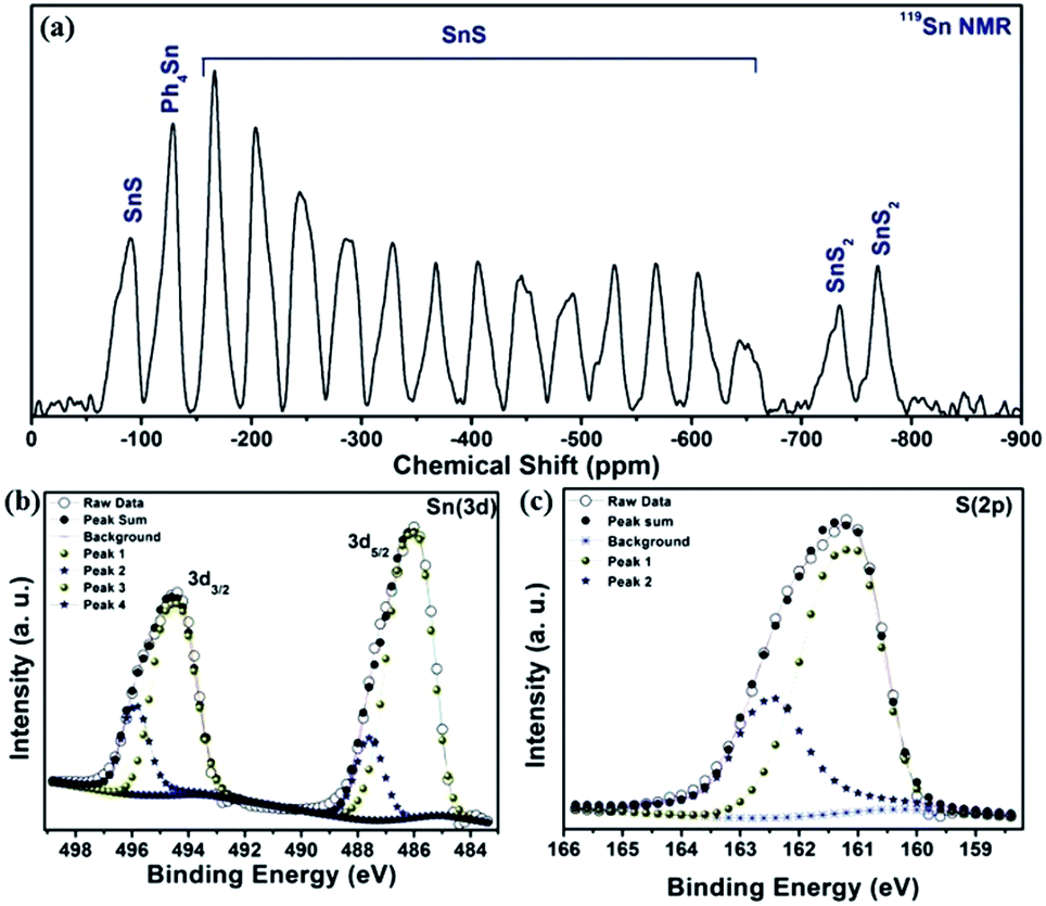 | ||
| Fig. 2 (a) 119Sn solid-state CP-MASS NMR spectrum of SnS NRs, (b) X-ray photoelectron spectra (XPS) for Sn (3d) and (c) for S (2p) of SnS NRs. | ||
The phases, elements and their oxidation states have been confirmed by an X-ray photoelectron spectroscopy (XPS) study, recorded here with Mg Kα. The survey scan of the sample is shown in Fig. S. I. 1 (in the ESI†), and indicates the presence of S (2s), S (2p), Sn (3d5/2), Sn (3d3/2), Sn (3p3/2) and Sn (3p1/2) energy states and a peak for Sn (3d) plasmon loss at 225.25 eV, 161.4 eV, 485.97 eV, 494.4 eV, 716.2 eV, 758.5 eV and 510.5 eV, respectively. High resolution XPS scans for tin and sulfur, shown in Fig. 2(b) and (c), reveal the presence of two valence states for the tin and sulfur atoms. After deconvolution of the XPS spectra for the binding energy peak of tin (3d energy state), as shown in Fig. 2(b), the binding energy peak positions are estimated to be at 485.92 eV and 487.58 eV (3d5/2), and 494.38 eV and 495.82 eV (3d3/2) energy states, respectively. The binding energy peaks at 485.92 eV (3d5/2) and 494.38 eV (3d3/2) again confirm the presence of Sn2+, while the binding energy peaks at 487.58 eV (3d5/2) and 495.82 eV (3d3/2) confirm the presence of Sn4+. Similarly, binding energy peaks corresponding to the sulfur (2p) energy state are at 162.42 eV and 161.06 eV. The peak at 162.42 eV indicates that the sulfur is attached to Sn4+, while the peak at 161.06 eV indicates attachment of the sulfur to Sn2+. Here, XPS analysis conclusively confirms the presence of SnS (as major) and SnS2 (impurity) phases in the material.
As mentioned previously, the morphology of the nanomaterial has a crucial impact on the properties of the material. So, the morphology as a function of reaction time has been studied by FEG-TEM and FEG-SEM experiments. The FEG-SEM micrographs are shown in Fig. 3(a) and (b) and Fig. S. I. 2 (in the ESI†). They show that well-distributed single crystalline NRs of SnS are formed during the solvothermal synthesis with a high aspect ratio. High resolution FEG-TEM images, as shown in Fig. 3(c), allow us to identify the lattice fringes for [111] and [210] planes with the inter-atomic d-spacing of 2.95 Å and 3.19 Å, respectively.
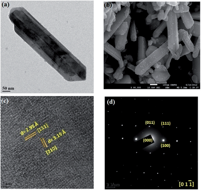 | ||
| Fig. 3 Electron microscopy patterns of SnS NRs synthesized at 160 °C: (a) FEG-TEM image of single SnS NRs, (b) FEG-SEM image, (c) high resolution lattice fringe and (d) SAED pattern from zonal axis [0 1 −1]. | ||
A Selected Area Electron Diffraction (SAED) measurement of the SnS nanorods (as shown in Fig. 3(a)) was taken and is shown in Fig. 3(d). The SAED pattern in Fig. 3(d) qualifies the single crystalline nature of NRs with dots for the [011], [100] and [111] planes. The zonal axis of this dotted pattern was found to be [0 1 −1].
3.1 Growth mechanism of NRs and the effect of solvothermal temperature
The tin atom in SnS is in the +II oxidation state and has an inert lone pair in its 5s orbital, which plays a crucial role in deciding the nature of the crystal growth. The lone pair of the 5s orbital is chemically inactive, but remains sterically active and plays an important role in the distortion of the normal rock salt structure due to its steric effect.49,50The lone pair forces the crystal to grow in an elongated [100] direction51 with successive layers between two SnS molecules along the a-axis, as shown in Fig. 1(c). In our case, solvothermal conditions lead to the growth of various kinds of NRs, as shown in the possible growth mechanism schematics in Fig. 4. This growth may be attributed to the inert lone pair effect of Sn(II) to direct growth in the a-axis direction.
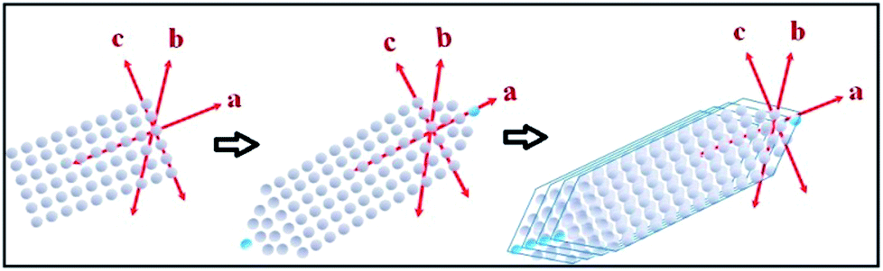 | ||
| Fig. 4 Schematics showing possible crystal growth mechanisms of SnS nanorods. | ||
Similarly, the solvothermal temperature has an impact on crystal growth in the b-axis direction and results in different aspect ratios of the facets in the NRs. The proposed growth mechanism has been assumed to be followed by initial nucleation of the SnS monoatomic layers in the a- and c-axis directions, i.e. the [a–c] plane. Soon after, atoms are added in the a-axis direction in such a way as to form tapering ends, which minimize the lattice face surface energy.51 The first step growth occurs in the [101] direction with an energy minimization process of the facets in the same direction, as shown in Fig. 4. Furthermore, growth of the next layers always occurs in the same [101] direction on top of the first layer, which leads to an increase in the b-axis direction. After some time, the growth of layers terminated much earlier than was required, leading to the generation of a ‘kink’ in the terminal position of the nanorod, as shown in the FEG-TEM image in Fig. 6(a). These growth patterns are mostly affected by the surface energy of the facets and by varying the synthesis temperature, one could expect to exert a possible effect on the crystal growth direction.
Furthermore, four solvothermal temperatures (from 140 °C to 200 °C) have been applied to study the changes in the NRs’ facet morphology. To study the comparative growth with change in solvothermal temperature, their corresponding PXRD data has been compared in Fig. 5, which shows prominent changes in the relative peak intensities of the (111) plane and (400) plane. As we can observe in Fig. 5, the peak intensities corresponding to the (400) and (202) planes increase with respect to the peak intensities of the (111) and (020) planes, respectively, as a function of solvothermal temperature. Similarly, the peak intensities corresponding to the coaxial planes, e.g. the (102) and (103) planes, also increase with increasing solvothermal temperature. Changes in peak intensity clearly reflect the preferential crystal growth which results in changes in the dimensions of the facets in SnS NRs. The face width of NRs in the (a–c) plane, in the b-direction, has reduced with increasing solvothermal temperature. The b-axis width is higher in the nanorods synthesized at 140 °C, while the rods become more symmetric in nature with an increase in temperature to 160 °C, as shown in the TEM images in Fig. 6(a) and (b) and the schematics of the SnS NRs in Fig. 5. Upon further increasing the solvothermal temperature from 160 °C to 180 °C, the (a–c) plane face width in the b-direction has started decreasing with the relative elongation in the (a–c) plane and the facet width has decreased to almost zero at 200 °C, as shown in Fig. 6(c) and (d). This morphological change also shows the impact in absorption band edge of the material during optical property testing.
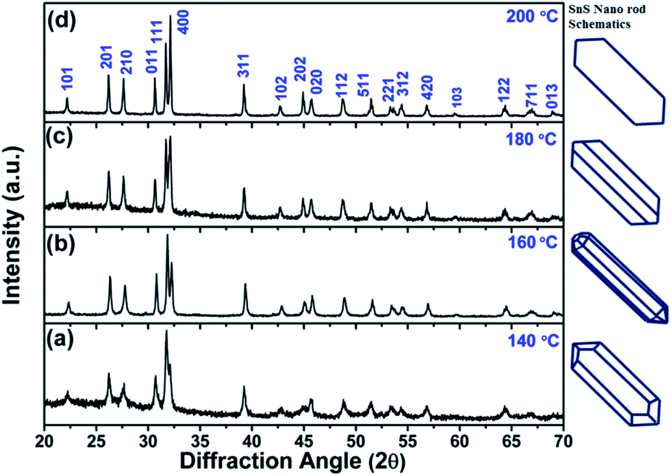 | ||
| Fig. 5 Powder X-ray diffraction patterns of SnS nanorods synthesized at (a) 140 °C, (b) 160 °C, (c) 180 °C and (d) 200 °C. | ||
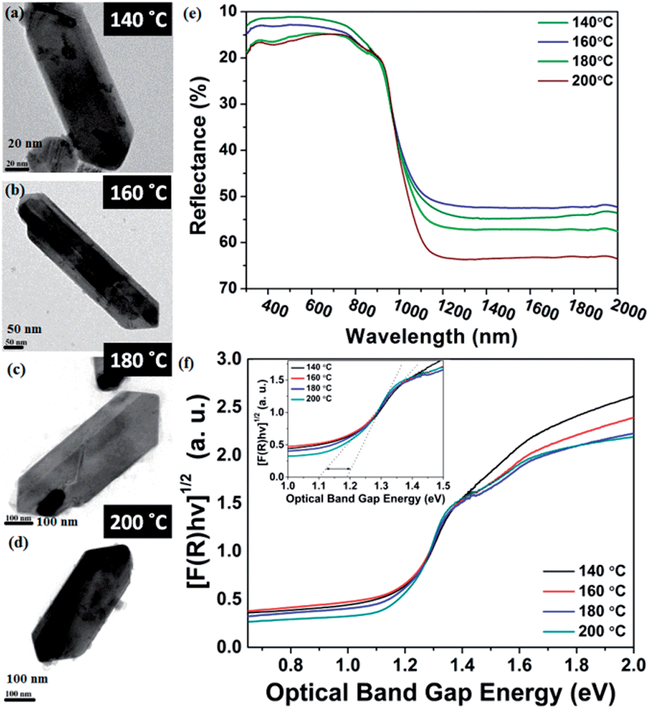 | ||
| Fig. 6 Optical property and FEG-TEM images of SnS NRs synthesized at (a) 140 ˚C, (b) 160 ˚C, (c) 180 ˚C and (d) 200 ˚C. (e) Reflectance vs. wavelength plot. (f) Band gap measurement with help of (αhν)1/2 vs. Eg plot (Tauc’s plot) | ||
3.2 Optical properties
SnS is a IV–VI semiconductor and its optical properties are of interest because of its several optoelectronic applications, such as holographic recording, near-infrared detector, solar absorber and the Hall effect.52–56 A material’s optical properties depend on the optical band edge, which can vary with changes in shape, size, strain, doping and surface modifications.53The impact of the nanosize of the facets on the physical properties of SnS has been studied by diffuse reflectance spectroscopy. It is always expected that nanomaterials have different atomic arrangements from their bulk counterparts, resulting in a different confinement level of the electrons, which results in variations in their optical properties.57,58 In the case of nanorods, the electron confinement is possible when either the diameter of the rod, the length of the rod, or both, have sizes below or on the order of their Bohr's radii.
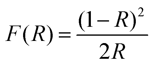
The diffuse reflectance spectra in Fig. 6 clearly show that all the SnS NRs have an absorption edge in the range of visible light. The notable point in Fig. 6(e) is that the ending of the absorption edge around 1000 nm varies for different SnS NRs prepared at different temperatures. To calculate the optical band gap, a Tauc plot has been generated and shown in Fig. 6(f) for the indirect band edge. The reflectance (R) value has been converted to the equivalent absorption extinction coefficient value F(R) by using the Kubelka–Munk transformation and is shown in the equation below.59,60
The variation of the band edge with changes of the nanorod facets clearly shows the dependence of the facet width on the solvothermal temperature. The NRs with the higher facet width (synthesized at 140 °C) have a band gap ∼1.1 eV, while those with a diminished facet width (synthesized at 200 °C) show an increase of the band edge to ∼1.2 eV, which is visible in the inset image of Fig. 6(f).
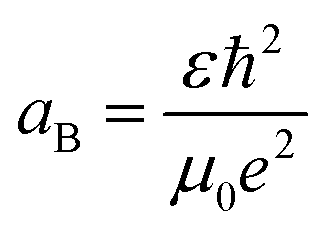
Furthermore, the Bohr's radius (aB) of the tin sulfide (SnS) has been calculated to be 7.24 nm, using the relationship shown in the equation,
3.3 Study of lithium storage
The charge–discharge behaviour of the SnS NRs has been tested with standard PVDF and CMC binders at a current rate of 160 mA g−1 in between the potential window of 0.01 V to 1.2 V against Li/Li+ at 20 °C. The discharge capacity of the PVDF binder electrode is found to be 385 mA h g−1 after the 50th discharge cycle, which is near to the theoretical capacity of the graphite electrode (375 mA h g−1). The loss in the case of the PVDF binder electrode is more prominent after the 20th discharge cycle. Therefore, it is expected that the binder has an impact on capacity loss. Therefore, the electrode is then prepared with an interactive CMC binder, which has less elasticity than the PVDF and is mechanically much more compatible to alloy-based anodes.60The capacity loss with the CMC binder has been reduced quite significantly and the discharge capacity after the 50th cycle is found to be 591 mA h g−1, much higher than the theoretical capacity of graphite, as shown in Fig. 7(a). Therefore, CMC can be a better, greener and more eco-friendly binder for low cost electrode fabrication. To get more possible information on the cathodic and anodic reactions, a half-cell of Swagelok-type assembly was used for cyclic voltammetry experiments. In the first cycle of the cyclic voltammogram, as shown in Fig. 7(b), with CMC binder, a minor peak at ∼1.4 V is observed, which suggests the intercalation of Li in the SnS layers spacing, as shown in the structure of SnS in Fig. 1(c).61 Another intense peak during the reduction process at a potential of 1.12 V indicates the conversion of SnS to Sn and Li2S with the reaction of sulfur with lithium ions21,29 as shown in eqn (1) and (2).
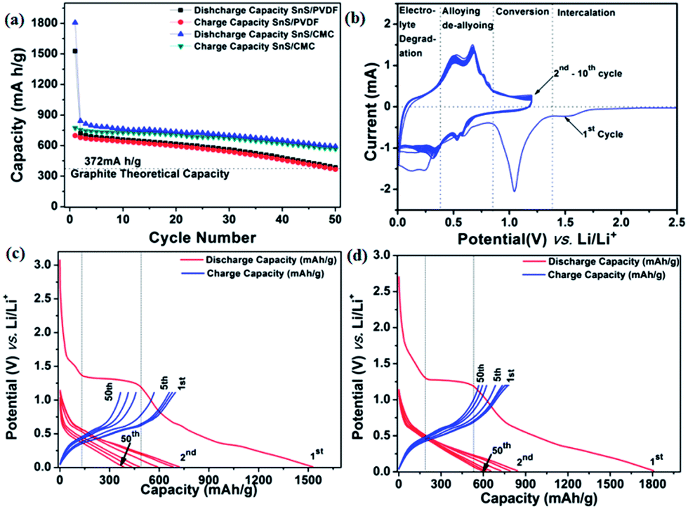 | ||
| Fig. 7 Electrochemical performance of SnS NRs. (a) Capacity vs. cycle number charge–discharge curve of SnS with PVDF and CMC binders, (b) cyclic voltammogram of SnS NRs with CMC binder, (c) potential vs. cycle number charge–discharge curve of SnS with PVDF binder and (d) potential vs. cycle number charge–discharge curve of SnS with CMC binder in potential window of 0.01V–1.2 V, against Li/Li+ at 20˚C. The current rate of 160 mA h g-1 has been used for the entire test. | ||
Upon further discharge, the reduction peak at a more negative potential of 0.6 V shows alloying of the Li with the Sn, as shown in eqn (3), which is shifted to 0.53 V and 0.57 V after the first cycle.36,39,42 This shift in alloying peak position after the first cycle is due to the formation of a solid electrolyte interface (SEI). Furthermore, the reduction peak at 0.25 V corresponds to the electrolyte degradation and SEI formation during electrochemical reduction.
| SnS + 2Li → Sn + Li2S | (1) |
| SnS2 + 4Li → Sn + 2Li2S | (2) |
| Sn + xLi → LixSn (x ≥ 4.4) | (3) |
On the reverse scan (oxidation process), oxidation occurred at 0.50 V and 0.66 V vs. Li/Li+ indicating a two-step dealloying reaction of the lithium from tin.36,39,42 From the second cycle onwards, the same peaks are showing almost constant peak current at 0.53 V and 0.57 V during reduction and corresponding peaks at 0.5 V and 0.66 V during oxidation at a scan rate of 0.1 mV s−1. This consistency in peak current shows the stability of the material in a Li-electrochemical environment and its practical compatibility in battery applications.
If we carefully observe the initial cycle performances of both electrodes, the differences in cycling arises during the first cycle. The first discharge capacity of the CMC binder electrode was found to be 1807.4 mA h g−1, while, with the PVDF binder electrode, the discharge capacity was found to be 1528 mA h g−1. Although both electrodes with different binders allow the lithium intercalation process at a potential of 1.4 V, as shown by a plateau in the discharge process in Fig. 7(c) and (d), they also contribute almost equal capacity to the first discharge cycle. The second cycle discharge capacity for the CMC binder electrode is 753.76 mA h g−1 and for the PVDF binder electrode is 721.38 mA h g−1. This trend shows that the binder property has a great effect on the primary reaction of active electrode materials with lithium. In this sequence, the CMC binder supports a more facile way to react lithium with electroactive material than PVDF. In the initial charge–discharge cycles, the coulombic efficiency of the PVDF-based electrode is higher than the CMC electrode and found to be 45.68% and 42.87%, respectively. However, upon further cycling, the coulombic efficiency of the CMC-based electrode is showing an increasing trend, as shown in Fig. S. I. 3(a) (ESI†), which may be another reason for better capacity retention in the present case. This further concludes that the CMC binder is a better binder for maintaining large volume expansion/contraction during charge–discharge processes in a tin–chalcogenide system.
To check the compatibility of the SnS–CMC electrode with high rates, the same electrode material was cycled at a rate of 350 mA g−1 for 50 cycles. The results showed that the first discharge capacity of 1379.8 mA h g−1 with a coulombic efficiency of approximately 44.13% is achieved with the SnS–CMC electrode. The second discharge capacity is found to be 702.06 mA h g−1 and after the 50th cycle, the capacity is found to be 564.72 mA h g−1, which is similar to that at a low current rate like 160 mA g−1. The only difference observed is that the coulombic efficiency is reduced to 85.99% at 350 mA g−1, while at 160 mA g−1, it is 95.96% (Fig. S.I. 3(b) in the ESI†). The improvement in coulombic efficiency in the cases of low and high current is interesting and drives us in another interesting direction. After collecting all the experimental evidence and explanations to the above fact, we will discuss this further in another report.
To check the compatibility of the SnS–CMC electrode with rate fluctuations, a cell was run at a sequential current rate of 100 mA h g−1, 300 mA h g−1, 500 mA h g−1, 700 mA h g−1 and 100 mA h g−1 for 5 cycles at each current rate and the results are shown in Fig. 8. The first discharge capacity is found to be 1449.9 mA h g−1 at the current rate of 100 mA g−1 with a coulombic efficiency of 42%. At end of the 5th cycle, the discharge capacity is found to be 640 mA h g−1 with an increased coulombic efficiency of 94.5%. After the next 5 cycles, the discharge capacities were found to be 537 mA h g−1 (current rate of 300 mA h g−1), 480 mA h g−1 (current rate of 500 mA g−1) and finally 256 mA h g−1 (at a current rate of 700 mA h g−1). Thereafter, the current rate was lowered to 100 mA h g−1 and the electrode regained its capacity of 600 mA h g−1. This regain in capacity, which is higher than the theoretical capacity of graphite, after large current perturbations shows that the material is a possible option for high rate compatible materials.
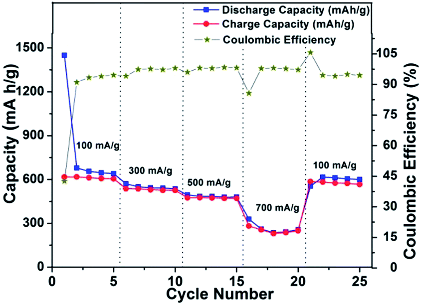 | ||
| Fig. 8 Power plot with coulombic efficiency for SnS nanorods–CMC electrode in a potential window of 0.01–1.2 V vs. Li/Li+ at 20 °C. | ||
In addition, to provide confirmation of the structural stability and the role of the binder in battery performance, ex situ TEM has been performed after 50 cycles of charge–discharge. It is observed that the shape of the rod is destroyed after 50 charge–discharge cycles, having been converted to small nanoparticles homogeneously distributed in the binder matrix, as shown in Fig. 9. A similar trend has been also observed for other alloy-based anodes (SnO2 nanorod,62,63 Si nanorod,64 SnSb alloy,65 SnNi anodes66) and in conversion anodes (CoO2,67 CuO68) used in lithium-ion batteries. Therefore, during the lithiation process, lithium intercalation occurs first, forming an alloy with the tin sulphide rods and causing a swell in volume.63,65 Upon subsequent de-intercalation, the 1D structure is destroyed, resulting in nanoparticles.
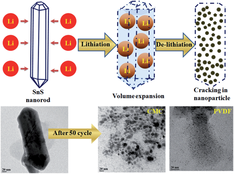 | ||
| Fig. 9 Schematics and TEM images of SnS nanorods before and after charge–discharge cycling. | ||
The breakdown of rod shape and formation of small nanoparticles in the initial cycles of charge–discharge play an important role in battery cycling. As the TEM images show in Fig. 9, the size of the nanoparticles are bigger in the case of the CMC binder in comparison with the PVDF binder. This conclusively reveals the fact that the volume expansion and particle holding capacity of the CMC binder-based electrode is higher than that of the PVDF binder electrode. It has also been experimentally proven that the CMC binder has more stiffness compared with the PVDF binder because CMC is very poor at absorbing the electrolyte used in batteries in comparison with PVDF and hence leads to less expansion and degradation of the binder.69 In our case, the bigger size of fractured particles after 50 cycles in the case of CMC compared with PVDF shows that CMC is holding its elastic property for a longer cycle life, which results in better holding of the active material and carbon matrix together and manages mechanical stress during cycling in the electrode. In other words, PVDF is known to absorb the electrolyte and the binder will swell and become less effective in holding the mechanical stress, resulting in smaller particle size after 50 cycles. In our group, we are constantly working in this direction to find out the underlying property that is responsible for this electrode quality improvement.
4. Conclusion
In summary, this work is based on using the solvothermal method to prepare highly crystalline SnS NRs with distinct facets. In this paper, we have attempted to understand the phase information using different physical measurements and draw a conclusion that the prepared sample is a mixture of SnS (major) and SnS2 (minor). Most of the previous reports in this field have not discussed the phase purity and reported the materials mostly as SnS2, but not SnS. It has been observed that the solvothermal temperature has an immense role in changing the crystal facets of the nanorods, which leads to changes in the optical properties. The nanorod morphology has been found suitable as an energy efficient anode material in lithium ion battery applications. The electrochemical performance with two different binders of PVDF and CMC has been tested. The compatibility of the material is quite pronounced with the CMC binder compared with PVDF binder for electrochemical energy storage.Acknowledgements
This manuscript is based upon work supported in part under the US-India Partnership to Advance Clean Energy-Research (PACE-R) for the Solar Energy Research Institute for India and the United States (SERIIUS), funded jointly by the U.S. Department of Energy (Office of Science, Office of Basic Energy Sciences, and Energy Efficiency and Renewable Energy, Solar Energy Technology Program, under Subcontract DE-AC36-08GO28308 to the National Renewable Energy Laboratory, Golden, Colorado) and the Government of India, through the Department of Science and Technology under Subcontract IUSSTF/JCERDC-SERIIUS/2012 dated 22nd Nov. 2012. The authors are indebted to SAIF, IIT-B for their assistance in Raman, HR-TEM and FEG-SEM analysis and thankful to Prof. A. Roychoudhury for XRD analysis and Dr Nalini G. Sundaram for useful discussions.References
- Y. Li, X. Y. Yang, Y. Feng, Z. Y. Yuan and B. L. Su, Crit. Rev. Solid State Mater. Sci., 2012, 37, 1–74 CrossRef.
- M. R. K. Ali, B. Snyder and M. A. El-Sayed, Langmuir, 2012, 28, 9807–9815 CrossRef CAS PubMed.
- D. B. Tice, D. J. Weinberg, N. Mathew, R. P. H. Chang and E. A. Weiss, J. Phys. Chem. C, 2013, 117, 13289–13296 CAS.
- M. Z. Ahmad, A. Z. Sadek, K. Latham, J. Kita, R. Moss and W. Woldarski, Sens. Actuators, B, 2013, 187, 295–300 CrossRef CAS PubMed.
- A. Dev, S. K. Panda, S. Kar, S. Chakrabarti and S. Chaudhuri, J. Phys. Chem. B, 2006, 110, 14266–14272 CrossRef CAS PubMed.
- B. Tang, G. Wang, L. Zhuo, J. Ge and L. Cui, Inorg. Chem., 2006, 45, 5196–5200 CrossRef CAS PubMed.
- H. S. Song, S. L. Li, L. Gao, Y. Xu, K. Ueno, J. Tang, Y. B. Cheng and K. Tsukagoshi, Nanoscale, 2013, 5, 9666–9670 RSC.
- Z. Deng, D. Cao, J. He, S. Lin, S. M. Lindsay and Y. Liu, ACS Nano, 2012, 6, 6197–6207 CrossRef CAS PubMed.
- P. D. Antuzen, J. J. Buckley and R. L. Brutchey, Nanoscale, 2011, 3, 2399–2411 RSC.
- S. E. Habas, H. A. S. Platt, M. F. A. M. Van Hest and D. S. Ginley, Chem. Rev., 2010, 110, 6571–6594 CrossRef CAS PubMed.
- L. A. Falkovsky, Phys.-Usp., 2008, 51, 887–897 CrossRef CAS PubMed.
- A. D. W. Todd, P. P. Ferguson, M. D. Fleischauer and J. R. Dhan, Int. J. Energy Res., 2010, 34, 535–555 CrossRef.
- F. Gillot, J. Oro-Sole and M. R. Palacin, J. Mater. Chem., 2011, 21, 9997–10002 RSC.
- J. Cabana, Z. Stoeva, J. J. Titman, D. H. Gregory and M. R. Palacine, Chem. Mater., 2008, 20, 1676–1678 CrossRef CAS.
- P. Poizot, S. Laruelle, S. Grugeon, L. Dupont and J. M. Tarascon, Nature, 2000, 407, 496–499 CrossRef CAS PubMed.
- P. S. Veluri and S. Mitra, RSC Adv., 2013, 3, 15132–15138 RSC.
- M. S. Chandrasekar and S. Mitra, Electrochim. Acta, 2013, 92, 47–54 CrossRef CAS PubMed.
- Y. Lu, J. P. Tu, J. Y. Xiang, X. L. Wang, J. Zhang, Y. J. Mai and S. X. Mao, J. Phys. Chem. C, 2011, 115, 23760–23767 CAS.
- M. V. Reddy, G. V. Subba and B. V. R. Chowdari, Chem. Rev., 2013, 113, 5364–5457 CrossRef CAS PubMed.
- E. Khon, K. Lambright, R. S. Khnayzer, P. Moroz, D. Perera, E. Butaeva, S. Lambright, F. N. Catellano and M. Zamkov, Nano Lett., 2013, 13, 2016–2023 CrossRef CAS PubMed.
- D. R. Cummins, H. B. Russell, J. B. Jasinki, M. Menon and M. K. Sunkara, Nano Lett., 2013, 13, 2423–2430 CrossRef CAS PubMed.
- Q. Li and R. M. Penner, Nano Lett., 2005, 5, 1720–1725 CrossRef CAS PubMed.
- Y. Yu, Y. Li, L. Liu, L. Su, Y. Zhang and L. Cao, Sci. Rep., 2013, 3, 1–6 Search PubMed.
- C. H. Lai, M. Y. Lu and L. J. Chen, J. Mater. Chem., 2012, 22, 19–30 RSC.
- Y. Du, Z. Yin, J. Zhu, X. Huang, X. J. Wu, Z. Zeng, Q. Yan and H. Zhang, Nat. Commun., 2012, 3, 1177 CrossRef PubMed.
- T. Jiang and G. A. Ozin, J. Mater. Chem., 1998, 8, 1099–1108 RSC.
- T. Momma, N. Shiraishi, A. Yoshizawa, T. Osaka, A. Gedanken, J. Zhu and L. Sominski, J. Power Sources, 2001, 97–98, 198–200 CrossRef CAS.
- J. W. Seo, J. T. Jang, S. W. Park, C. Kim, B. Park and J. Cheon, Adv. Mater., 2008, 20, 4269–4273 CrossRef CAS.
- Z. Jiang, C. Wang, G. Du, Y. J. Zhong and J. Z. Jiang, J. Mater. Chem., 2012, 22, 9494–9496 RSC.
- Y. Zou and Y. Wang, ACS Nano, 2011, 5, 8108–8114 CrossRef CAS PubMed.
- P. Wu, N. Du, H. Zhang, J. Liu, L. Chang, L. Wang, Y. Deren and J. Z. Jiang, Nanoscale, 2012, 4, 4002–4006 RSC.
- M. J. Powell, E. A. Marseglia and W. Y. Liang, J. Phys. C: Solid State Phys., 1978, 11, 895–904 CrossRef CAS.
- S. G. Patil and R. H. Tredgold, J. Phys. D: Appl. Phys., 1971, 4, 718–722 CAS.
- S. H. Choi and Y. C. Kang, Small, 2014, 3, 474–478 CrossRef PubMed.
- K. Aso, A. Hayashi and M. Tatsumisago, Cryst. Growth Des., 2011, 11, 3900–3904 CAS.
- D. D. Vaughn, O. L. Hentz, S. Chen, D. Wang and R. E. Schaak, Chem. Commun., 2012, 48, 5608–5610 RSC.
- J. Lu, C. Nan, L. Li, Q. Peng and Y. Li, Nano Res., 2013, 6, 55–64 CrossRef CAS PubMed.
- J. Cai, L. Zesheng and P. K. Shen, ACS Appl. Mater. Interfaces, 2012, 4, 4093–4098 CAS.
- J. G. Kang, J. G. Park and D. W. Kim, Electrochem. Commun., 2010, 12, 307–310 CrossRef CAS PubMed.
- L. Wu, X. Hu, J. Qian, F. Pei, F. Wu, R. Mao, X. Ai, H. Yang and Y. Cao, J. Mater. Chem. A, 2013, 1, 7181–7184 CAS.
- Y. Liu, X. H. Liu, B. M. Nguyen, J. Yoo, J. P. Sullivan, S. T. Picraux, J. Y. Huang and S. A. Dayeh, Nano Lett., 2013, 13, 4876–4883 CrossRef CAS PubMed.
- J. Rodriguez-Carvajal, Phys. B, 1993, 192, 55–69 CrossRef CAS.
- V. E. Zorin, GSim – visualisation and processing tool for NMR experiments and simulations, http://gsim.sourceforge.net.
- A. V. Murugan, T. Muraliganth and A. Manthiram, Electrochem. Commun., 2008, 10, 903–906 CrossRef PubMed.
- H. G. Choi, Y. H. Jung and K. Kim, J. Am. Ceram. Soc., 2005, 88, 1684–1686 CrossRef CAS.
- H. R. Chandrasekhar, R. G. Humphreys, U. Zwick and M. Cardona, Phys. Rev. B: Solid State, 1977, 15, 2177–2183 CrossRef CAS.
- D. G. Mead and J. C. Irwin, Solid State Commun., 1976, 20, 885–887 CrossRef CAS.
- M. Cruz, J. Morales, J. P. Espinos and J. Sanz, J. Solid State Chem., 2003, 175, 359–365 CrossRef CAS.
- A. J. Biacchi, D. D. Vaughn and R. E. Schaak, J. Am. Chem. Soc., 2013, 135, 11634–11644 CrossRef CAS PubMed.
- A. Walsh and G. W. Watson, J. Phys. Chem. B, 2005, 109, 18868–18875 CrossRef CAS PubMed.
- G. Z. Wulff, Kristallogr. Mineral., 1901, 34, 449–530 CAS.
- W. Albers, C. Haas, H. J. Vink and J. D. Wasscher, J. Appl. Phys., 1961, 32, 2220–2225 CrossRef CAS PubMed.
- G. A. Tritsaris, B. D. Malone and E. Kaxiras, J. Appl. Phys., 2013, 113, 233507 CrossRef PubMed.
- M. M. Nassary, J. Alloys Compd., 2005, 398, 21–25 CrossRef CAS PubMed.
- L. A. Burton and A. Walsh, Appl. Phys. Lett., 2013, 102, 132111 CrossRef PubMed.
- C. Haas and M. G. Corbey, J. Phys. Chem. Solids, 1961, 20, 197–203 CrossRef CAS.
- A. L. Efros and M. Rosen, Annu. Rev. Mater. Sci., 2000, 30, 475–521 CrossRef CAS.
- C. Burda, X. Chen, R. Narayanan and M. A. El-Sayed, Chem. Rev., 2005, 105, 1025–1102 CrossRef CAS PubMed.
- W. E. Vargas, J. Opt. A: Pure Appl. Opt., 2002, 4, 452–456 CrossRef.
- W. J. Zhang, J. Power Sources, 2011, 196, 13–24 CrossRef CAS PubMed.
- F. Robert, P. E. Lippens, J. O. Fourcade, J. C. Jumas and M. J. Morcrette, J. Power Sources, 2005, 146, 492–495 CrossRef CAS PubMed.
- Y. Wang and J. Y. Lee, J. Phys. Chem. B, 2004, 108, 17832–17837 CrossRef CAS.
- J. Y. Huang, L. Zhong, C. M. Wang, J. P. Sullivan, A. Subramanian, H. Fan, L. Qi, A. Kushima and J. Li, Science, 2010, 330, 1515–1519 CrossRef CAS PubMed.
- R. Ruffo, S. S. Hong, C. K. Chan, R. A. Huggins and Y. Cui, J. Phys. Chem. C, 2009, 113, 11390–11398 CAS.
- J. O. Besenhard, J. Yang and M. Winter, J. Power Sources, 1997, 68, 87–90 CrossRef CAS.
- H. Mukaibo, T. Momma and T. Osaka, J. Power Sources, 2005, 146, 457–463 CrossRef CAS PubMed.
- P. Poizot, S. Laruelle, S. Grugeon, L. Dupont and J. M. Tarscon, Nature, 2000, 407, 496–499 CrossRef CAS PubMed.
- J. Wang, Y. C. K. C. Wiegart and J. Wang, Chem. Commun., 2013, 49, 6480–6482 RSC.
- I. Kovalenko, B. Zdyrko, A. Magasinski, B. Hertzberg, Z. Milicev, R. Burtovyy, I. Luzinov and G. Yushin, Science, 2011, 334, 75–79 CrossRef CAS PubMed.
Footnote |
| † Electronic supplementary information (ESI) available: Survey scan of X-ray photoelectron spectroscopy, TEM image of SnS synthesised at 160 °C, coulombic efficiency plot and charge–discharge curve at 350 mA g−1 current rate. See DOI: 10.1039/c3ra46308g |
| This journal is © The Royal Society of Chemistry 2014 |