C. Jiangab,
R. R. Luntac,
P. M. Duxburya and
P. P. Zhang*ac
aDepartment of Physics and Astronomy, Michigan State University, East Lansing, MI 48824, USA. E-mail: zhang@pa.msu.edu
bDepartment of Chemistry, Michigan State University, East Lansing, MI 48824, USA
cChemical Engineering and Materials Science, Michigan State University, East Lansing, MI 48824, USA
First published on 27th November 2013
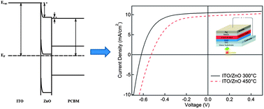
ZnO is a versatile cathode buffer layer for organic photovoltaics (OPV) due to its appealing optical and electronic properties. Using the sol–gel method, we find that the processing temperature of ZnO cathode buffer layers significantly influences the device performance of inverted polymer OPVs composed of blended films of poly(3-hexylthiophene) (P3HT) and [6,6]-phenyl-C61-butyric acid methyl ester (PCBM). In particular, ZnO processed at relatively low temperatures results in better device performance than those processed at higher temperatures despite the improved crystallinity and electron mobility of the latter. We attribute this finding to the tuning of the ZnO work function with the annealing temperature, which determines the interface energetics at the cathode and thus influences the open circuit voltage, series resistance and fill factor.
Interfacial buffer layers therefore play a critical role in adjusting the contact properties between active layers and electrodes. For instance, in the presence of non-ohmic contacts in bulk heterojunction (BHJ) devices, injection barriers may give rise to a reduction of the internal electric field and a decrease in Voc,13,14 while interfacial buffer layers can be readily utilized to optimize these contacts.15–17 Additionally, interfacial buffer layers may contribute to enhancement of the charge collection and reduction of the interfacial contact resistance and charge recombination, leading to smaller series resistance (Rseries), larger shunt resistance (Rshunt), and hence improved performance.3,6,7,18,19
Among the n-type buffers used in inverted structures,3,20–24 ZnO offers the advantages of high conductivity, excellent optical transparency and environmental stability.17,25,26 Various preparation methods have been utilized to fabricate high-quality ZnO films in planar and nanowire configurations for solar cell applications.27–34 Among them, spin coating with the sol–gel method is considered to be cost effective and compatible with solution processing of organic solar cells. The sol–gel method also allows for ZnO-based nanostructuring,35,36 elemental doping,19,37 and surface modification,7,38 to improve the ZnO functionality. Here we focus on inverted OPVs with the planar ZnO cathode buffer layer fabricated by the sol–gel method from zinc acetate decomposition. Several parameters can be tuned in the sol–gel process to improve the ZnO thin film morphology, as well as its optical and electrical properties. However there have been conflicting reports of this optimization in the literature.18,39 Moreover, optimal annealing temperatures reported in the literature range widely from 150 to 450 °C,4,18,33,34,39–46 although it is recognized that low temperature annealing is more compatible with the processing of plastic organic solar cells. Therefore, thorough investigation of the characteristics of ZnO buffer layers is necessary.
In this article, we report the effects of ZnO processing temperature on the photovoltaic properties of inverted solar cells with the structure of ITO/ZnO/P3HT:PCBM/MoO3/Ag. We find that the formation of the ZnO cathode buffer layer at 300 °C results in the best device performance with an average power conversion efficiency of ∼4% despite the improvement in thin film crystallinity and electron mobility for samples annealed at even higher temperatures. We attribute this phenomenon to the tuning of the ZnO work function, monitored with Kelvin Probe force microscopy, which determines the interface energetics and leads to an improved ohmic contact at the low-temperature processed ITO/ZnO cathode. With the enhanced charge collection and electronic coupling at the contact, the open circuit voltage (Voc), sheet resistance (Rs) and filled factors (FF) are all improved.
ZnO film preparation was followed by spin-coating a poly(3-hexylthiophene) (P3HT) and PCBM blend (1:
0.8 in weight) in chlorobenzene (27 mg ml−1 in total) at 800 RPM for 30 s. P3HT and PCBM were purchased from Rieke Metal and American Dye Sources Inc., respectively. The samples were then heated to 105 °C at a rate of ∼20 °C min−1 and annealed at this temperature for 20 min, followed by cooling at a rate of ∼10 °C min−1 to room temperature. The entire process was carried out in a glove box where the oxygen and water impurity levels are below 0.1 ppm.
The resulting samples were transferred to a vacuum deposition chamber (Angstrom Engineering), where 10 nm MoO3 and 100 nm Ag were thermally deposited with shadow masks under a deposition pressure of ∼3.5 × 10⁻⁶ Torr. Solar cell efficiencies were characterized in air using a Keithley 2420 source-meter and a Newport solar simulator under 0.98 ± 0.01 kW m−2 illumination measured with an NREL calibrated mc-Si detector with KG5 filter. The mismatch factor of the solar simulator to the P3HT:PCBM based inverted cells was determined to be 1.07 ± 0.02 from the external quantum efficiency measurements.
ZnO buffer layer | Jsc (mA cm−2) | Voc (V) | FF | PCE (%) |
---|---|---|---|---|
0L at 300 °C | 9.7 ± 0.2 | 0.33 ± 0.01 | 0.43 ± 0.01 | 1.4 ± 0.1 |
1L at 300 °C | 10.5 ± 0.8 | 0.62 ± 0.01 | 0.60 ± 0.02 | 3.9 ± 0.3 |
2L at 300 °C | 10.4 ± 1.0 | 0.61 ± 0.02 | 0.58 ± 0.04 | 3.7 ± 0.6 |
3L at 300 °C | 10.2 ± 1.1 | 0.61 ± 0.02 | 0.59 ± 0.06 | 3.8 ± 0.8 |
0L at 450 °C | 9.6 ± 0.2 | 0.32 ± 0.01 | 0.41 ± 0.01 | 1.3 ± 0.1 |
1L at 450 °C | 9.7 ± 1.0 | 0.53 ± 0.04 | 0.52 ± 0.03 | 2.7 ± 0.5 |
2L at 450 °C | 9.7 ± 0.3 | 0.53 ± 0.03 | 0.52 ± 0.01 | 2.7 ± 0.2 |
3L at 450 °C | 9.6 ± 0.4 | 0.51 ± 0.04 | 0.51 ± 0.02 | 2.5 ± 0.3 |
ITO at 450 °C/1L at 300 °C | 10.1 ± 0.7 | 0.60 ± 0.02 | 0.58 ± 0.03 | 3.6 ± 0.3 |
It is well known that the optical and electrical properties of the ITO substrate can be sensitive to high temperature annealing. Accordingly, to eliminate the impact of ITO at higher annealing temperatures we performed control experiments with zinc acetate spun on pre-annealed (450 °C) and pristine ITO substrates, followed by 300 °C annealing of both to create ZnO thin films. The J–V curves of the two devices are plotted in Fig. 1(c), which show nearly identical performance, suggesting that any changes in the optical and electronic properties of ITO from the higher temperature annealing do not play a significant role here, distinct from an earlier report.46
To further distinguish the contributions of the interface quality and the ZnO thin film conductivity, we fabricated inverted devices with the ZnO buffer layer of various thickness via multiple spin-coatings followed by thermal annealing at each step. As presented in Fig. 2 and Table 1, devices without ZnO buffer layer show diminished performance, likely due to enhanced recombination at the cathode which decreases the shunt resistance, leading to reduced Voc and FF. Additionally, devices with the ZnO buffer layer processed at 300 °C consistently outperform those processed at 450 °C at each corresponding buffer layer thickness, where the different ZnO film thicknesses under a given annealing condition show similar performance in Voc and FF. This limited thickness dependence suggests that interface properties at the cathode are markedly influenced by the ZnO processing temperature and the resistance of the ZnO thin film plays a lesser role in determining the performance of the inverted devices.
![]() | ||
Fig. 2 J–V characteristics for devices based on 0 layer, 1 layer, 2 layers and 3 layers of ZnO buffer prepared at 300 and 450 °C, respectively. |
The optical transmittance of ITO/ZnO substrates is depicted in Fig. 3(a) where the low-temperature annealed substrate yields a higher transmittance than the high-temperature annealed one in the visible range. However, such a difference mainly originates from the ITO substrate, as illustrated by the similar transmittance between the bare ITO and the ITO/ZnO substrates annealed at 450 °C, respectively. This observation implies a limited impact of the ZnO optical properties on the OPV device performance as the films are very thin.
It has been well established that higher annealing temperatures lead to improved thin film crystallinity and enhanced electron mobility.41,47,51 As presented in the XRD data of ZnO thin films in Fig. 3(b), samples annealed at 300 °C show amorphous structures, whereas a pronounced ZnO (002) peak is observed in thin films processed at 450 °C. One may expect to obtain better electron transport, reduced Rseries and therefore enhanced fill factors in devices with high-temperature processed ZnO films. However, the devices processed at 300 °C show better performance, including fill factor which suggests that there are other dominant factors compensating the crystallinity and mobility effect. It is worth noting that annealing the ZnO buffer layer below 300 °C results in significantly reduced device performance, which likely stems from the incorporation of residue zinc acetate in the ZnO film as indicated by the thermogravimetric analysis (TGA) of zinc acetate (inset of Fig. 3(b)).
We have also investigated the roughness and homogeneity of ZnO thin films with AFM. Fig. 4(a) and (b) are AFM images of the single layer ZnO film prepared at 300 °C and 450 °C, respectively. The film prepared at 450 °C is rougher with a root-mean-square (rms) roughness of 2.2 nm as compared to the film prepared at 300 °C (rms of 1.7 nm), which might result in a higher leakage current (smaller Rshunt) and enhanced recombination between injected holes and photo-generated electrons at the cathode. However, this difference in roughness is unlikely to be the driving force for the performance difference we observed between various annealing conditions since the OPV device performance is not strongly dependent on the ZnO film thickness, as suggested in Fig. 2, even though the multiple layer coating is expected to improve the compactness of the ZnO film and thus reduces the leakage paths.
KPFM is a useful tool to measure the work function of electrodes and the interface energetics in solar cells.5,52,53 It is worth noting that oxygen molecules adsorbed on ZnO grain boundaries can trap free electrons and cause a depletion layer near the surface.54–56 Accordingly, the interface energetics between ZnO and photoactive materials and the resultant transport properties (in dark) in solar cell devices can be impacted. We found that light soaking using the solar illuminator is effective at removing these surface states, after which the dark current and the photocurrent merge together in the forward bias. The work functions obtained at such conditions are summarized in Table 2.
ZnO preparation temperature | ITO | ITO/ZnO | ITO/ZnO/PCBM |
---|---|---|---|
300 °C | 4.77 | 4.36 | 4.34 |
450 °C | 4.76 | 4.53 | 4.38 |
The energy level alignments between ITO, ZnO and PCBM from KPFM are shown in Fig. 5 where the depletion widths and band bending are inferred. One can see that the ZnO work function has been tuned by thermal treatment where the Fermi level in the 300 °C annealed film is positioned in closer proximity to the conduction band edge, as compared to the one annealed at 450 °C. This implies that the former sample is more heavily n-doped by native defects, including Zn interstitials and oxygen vacancies, that have been partially annihilated by annealing at higher temperatures due to the improved thin film crystallinity.51,57 Consequently, the width of the Schottky barrier formed at the ITO/ZnO interface may be significantly reduced in the 300 °C annealed sample, as shown in Fig. 5.
In addition, we find that the Fermi level of the ITO/ZnO cathode is pinned at the negative integer charge transfer state (EICT−) of PCBM for both samples within the experimental error. As shown in Fig. 5(a), in the 300 °C case, a neutral contact is formed at the ZnO/PCBM interface due to the alignment of energy levels between the cathode and PCBM. While for the ZnO film annealed at 450 °C, although its work function falls well within the transport gap of PCBM so that one may expect the vacuum level alignment at the interface,12 our results suggest that the Fermi level is still pinned at the EICT− of PCBM, leading to the formation of an interface dipole. Here we propose two possibilities to reconcile the discrepancy. First, the charge transfer behavior between ZnO and PCBM may be disturbed by the existence of interface gap states.11 Second, if the PCBM film is unintentionally doped by impurities, the imbalance in work functions upon contact with the ITO/ZnO cathode (450 °C) can be compensated by the electron flow from PCBM to the cathode.52,53
Finally, we discuss how the interface energetics affect the solar cell device performance. As presented in Table 1, the devices made of the 300 °C annealed ZnO cathode buffer display a higher FF, a larger PCE and an optimal Voc as obtained in the P3HT:PCBM systems with ohmic contacts.16,58 On the contrary, Voc, FF, and PCE are reduced by about 15%, 13%, and 31%, respectively in the devices composed of the 450 °C annealed ZnO film. Our studies suggest that there are several factors contributing to the enhanced performance in devices composed of the ZnO buffer layer processed at 300 °C. (1) Charge collection at the ITO/ZnO interface may be improved by electron tunneling through the Schottky barrier of reduced width; (2) the Fermi level of the ITO/ZnO cathode lines up with the EICT− of PCBM which enhances the electronic coupling at the interface and minimizes the Voc loss. In contrast, the extraction barrier at the ZnO (450 °C)/PCBM interface may result in a significant charge accumulation and the consequent recombination loss at the interface; (3) these two effects also contribute to the low contact resistance, thereby a smaller Rseries and a larger FF in the 300 °C case.
This journal is © The Royal Society of Chemistry 2014 |