Enhanced luminescence and charge separation in polythiophene-grafted, gold nanoparticle-decorated, 1-D ZnO nanorods

Sundaramurthy Jayaramanad, P. Suresh Kumarb, D. Mangalarajbc, D. Rajarathnama, Seeram Ramakrishnad and M. P. Srinivasan*a
aNational University of Singapore, Block E5, 4 engineering drive 4, 117576, Singapore. E-mail: chesmp@nus.edu.sg
bThin Film and Nanomaterials Laboratory, Department of Physics, Bharathiar University, Coimbatore 641 046, India
cDepartment of Nanoscience and Technology, Bharathiar University, Coimbatore 641046, India
dDepartment of Mechanical Engineering, National University of Singapore, Block E3, 2 Engineering Drive 3, 117576, Singapore

Received 20th October 2013 , Accepted 3rd February 2014

First published on 14th February 2014


Abstract

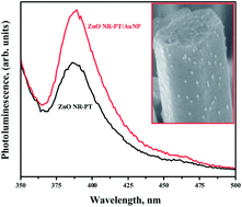
In this work, we demonstrate a facile method for fabricating hybrid organic/inorganic structures of vertically oriented 1-dimensional (1-D) ZnO nanorods (NR) coupled with regio-regular poly(3-(2-methoxyethoxy) ethoxymethyl) thiophene-2,5-diyl (PMEEMT). The NRs were synthesized by two-step solution processes and exhibited a hexagonal wurtzite structure with a lattice spacing of 0.248 nm. Cross-section analysis of field-emission scanning electron microscopy (FESEM) analysis confirmed the NRs were vertically oriented and densely packed with diameter of about 250 nm. The hybrid structures were formed by encapsulating the ZnO NRs with polythiophenes, thereby creating a direct heterojunction interface. These interfaces allowed easy electron transport along the NR avoiding loss of mobility due to grain boundary scattering; further, the large aspect ratio and surface area of NR increased the effective interface between polythiophene and the nanorods contributing to efficient charge separation. In addition, decoration of the ZnO hybrid structures by gold nanoparticles (AuNPs) induced enhanced luminescence properties. These functionalized organic/inorganic hybrid structures can pave the way for applications in photovoltaics and sensing.


Introduction

Organic/inorganic hybrid structures are promising systems for a variety of electronic applications due to the efficient intra-molecular energy and electron transfer between organic and inorganic moieties. Organic molecule-based devices based on conjugated polymers are still limited in their performance because of the weak absorption in the visible long wavelength, poor charge transport and low stability.1 In order to overcome some of these issues, bulk hetero-junction devices of p-type conjugated polymers in combination with n-type polymers or with n-type inorganic semiconductor metal oxides have been considered.2,3 The coupling can help to construct the devices with superior photovoltaic, electronic, magnetic, and optical properties.4 These hybrid structures have the advantage of easy solution processing, low-cost large area devices, large optical extinction coefficients, and enhanced carrier mobilities provided by the constituents namely, conjugated polymers and semiconductor metal oxides.5,6

Among metal-oxides, zinc oxide (ZnO) is considered as a promising n-type semiconductor because of its high electron mobility (100 cm2 V−1 s−1),7 band gap of 3.31 eV, feasibility of synthesizing at low temperature8 and exhibition of different morphologies such as nanoparticles, nanoribbons, nanorods and nanowires.9 Similarly, among conjugated polymers, polythiophene has been employed as a p-type semiconducting material because of its high charge carrier mobility (0.1 cm2 V−1 s−1), stability and easy solution processing.10,11 In bulk heterojunction devices, the morphology is an important criterion to enhance the interfacial area between the p–n junctions where the photo-generated excitons are dissociated into charge carriers which enables holes and electrons to be transported and collected.12 So, an ideal hybrid device is one in which donor and acceptor materials are arranged in a densely packed vertical array and the vertical alignment of these materials ensures a non-tortuous path for charge transport.13–15 Hence, the band alignment and surface chemistry across the polymer–inorganic interface are critically important. Briseno et al. successfully grafted the oligo- and polythiophenes on ZnO nanowires creating p–n junction solar cells with an efficiency of 0.036%.16 Olson et al. fabricated ZnO nanofibers using low temperature hydrothermal treatment and obtained 0.53% efficiency for spin coated poly(3-hexylthiophene) (P3HT) on mesoporous nanofibers.17 Zhang et al. demonstrated that the side-on attachment of polythiophene derivatives to ZnO nanowires promotes a co-axial polymer backbone-nanowire arrangement favouring high hole mobility.13 Xiaohui et al. reported the morphology of the hybrid structures with oriented zinc oxide pillars which played an important role in collecting the photogenerated electrons and acted as a conducting path to the electrode.15

In addition, AuNP-semiconductor hybrid nanomaterials have become an active frontier of research because of their remarkable optical, electrical, and catalytic properties.18 Au/ZnO nanocomposites with unique physical and chemical properties have been applied to dye-sensitized solar cells, field emission, luminescence, photocatalysis and biosensing.19,20 Chen et al. observed an increase in the efficiency of the gold-coated ZnO nanorod dye-sensitized solar cells from 0.7% to 1.2%.21 Haldar et al. showed the efficient fluorescence resonance energy transfer from Rhodamine 6G dye to Au@ZnO core shell nanoparticles.22 Chen et al. showed the potential of the ZnO/Au nanoarrays as a convenient and robust SERS-active substrate for food safety monitoring.23 The above and other examples in literature clearly convey the importance of creating effective direct interface between organic and inorganic moieties to improve the efficient charge separation. Hence, we adopted a simple way of fabricating hybrid organic/inorganic structures of vertically oriented 1-D ZnO NRs with surface encapsulated and grafted with a molecular thin layer of alkoxy regio-regular polythiophenes, thereby creating a direct heterojunction interface. We expect these synthesized ZnO NRs will allow easy electron transport along the NR avoiding loss of mobility due to grain boundary scattering. The large aspect ratio of NR can increase the effective infiltration of polythiophene molecules and contribute to efficient charge separation. Further, we expect the immobilization of AuNPs on ZnO hybrid structures to induce higher luminescence properties.

Experimental details

Materials

Zinc acetate dehydrate (Merck), hexamethylenetetramine (Merck), aqueous ammonia (synthesis grade) (Merck), regio-regular poly(3-(2-methoxyethoxy) ethoxymethyl) thiophene-2,5-diyl (PMEEMT) (Sigma-Aldrich) and gold(III) chloride trihydrate (Sigma-Aldrich) were used as received. Chloroform, methanol and acetone of HPLC grade were purchased from Tedia and were used as received. Silicon wafers from Engage Electronics Pte Ltd., Singapore were 0.6 mm thick, P-doped, polished on one side and with a natural oxide layer. Indium-tin oxide (ITO) coated glass slides with sheet resistance of 20 Ω cm, were purchased from Anhui Bengbu Huayi Conductive Film Glass Co., Ltd (China, PR).

Substrate preparation

Silicon wafers and glass slides were treated with a 7/3 (v/v) mixture of concentrated sulphuric acid and 30% hydrogen peroxide at 70 °C for 45 min. (Caution: “Piranha” solution reacts violently with many organic materials and should be handled with extreme care). The substrates were then rinsed with deionized water and methanol, and then finally blown dry with nitrogen. ITO substrates were treated with a 5[thin space (1/6-em)]:[thin space (1/6-em)]1[thin space (1/6-em)]:[thin space (1/6-em)]1 (v/v) solution of deionized water, 40% ammonia solution and 30% hydrogen peroxide at 80 °C for 1 h. The substrates were then rinsed with deionized water and acetone several times and blown dry with nitrogen.

Synthesis of ZnO seed layer and nanorods

Initially, zinc acetate dihydrate was dissolved in 40% aqueous ammonia to form a zinc ammonia complex solution to act as a zinc cation precursor. Distilled water at 80 °C was used as an anionic precursor. The successive ionic layer adsorption and reaction (SILAR) growth process has been adopted for the seed layer growth. This approach involves several deposition cycles of alternate immersion of the substrate in cationic and anionic solutions followed by a final rinse in distilled water at room temperature.24 The detailed reaction mechanism for the formation of ZnO seed layer is shown below.
 
[Zn(NH3)4]2+ + H2O → Zn2+ + NH4+ + OH (1)
 
Zn2+ + 2OH → Zn(OH)2 (2)
 
Zn(OH)2 → ZnO(solid) + H2O (3)

Firstly, the substrate was immersed in the cationic precursor solution resulting in the adsorption of the zinc ammonia complex ([Zn(NH3)4]2+) as a thin layer on the surface. Subsequent immersion in distilled water at 80 °C resulted in the conversion of adsorbed zinc ammonia complex into zinc hydroxide (Zn(OH)2) (eqn (1) & (2)). The Zn(OH)2 layer was rinsed in distilled water to remove loosely bound molecules. A time period of 20 and 80 s were maintained for each immersion step of cationic and anionic solutions and followed by a waiting time of 15 s. A uniform ZnO seed layer was obtained after 20 deposition cycles. The ZnO seed layer exhibited higher stability and reproducibility of films compared with spin coating.

ZnO NRs were grown from seed layers by chemical bath deposition. Equivalent amounts of 2 mM zinc acetate dihydrate and 2 mM hexamethylene tetraamine in aqueous solution were prepared and adjusted to pH 7. The as-prepared ZnO seed layer substrates were immersed vertically in the reaction solution at 85 °C for 8 h. The substrates were carefully rinsed in water and acetone several times before storing.

Self-assembly of PMEEMT and incorporation of AuNPs on ZnO NRs

ZnO NRs were immersed in a 2 mM solution of PMEEMT in chloroform for 12 h. Then the ZnO NRs were rinsed several times in chloroform and sonicated in chloroform for 3 min to remove unbound PMEEMT.

Gold nanoparticles (AuNP) were prepared by a standard method reported in the literature.25 Specifically, 1 mM of gold(III) chloride trihydrate was prepared in 30 ml of deionized water which was refluxed at 100 °C and stirred at 600 rpm for 10 min. 3 ml of 38.8 mM sodium citrate in deionized water was added to the refluxing solution. Stirring was continued for the next 45 min. The colour of the mixture evolved gradually from gray to purple and finally to wine red, indicating the formation of AuNPs. The synthesized AuNPs were deposited by an ex situ method i.e. immersing the PMEEMT-modified ZnO NRs into the AuNP solution for 4 h. Subsequently, the unbounded nanoparticles were removed by washing with deionized water. The films were dried in nitrogen and stored.

Device fabrication and photocurrent measurements

In a typical device structure, the PMEEMT and ZnO NR were used as p- and n-type materials, respectively. These p–n junctions of PMEEMT/ZnO hybrid structures were fabricated as shown in Fig. 8a. 50 nm thick Au electrodes were deposited on the top of ZnO/PMEEMT structure through a shadow mask. The photocurrent measurements were performed and compared in dark and under AM1.5 irradiation (100 mW cm−2), using a XES-151 S solar simulator (San-Ei, Japan).

Characterization

The crystallographic information of the as-prepared ZnO samples was investigated by X-ray diffraction (Shimadzu XRD-6000 with Cu Kα1 radiation (k = 1.5406 Å) from 20 to 80° at a scanning speed of 3° min−1). The surface morphology of the ZnO samples, energy-dispersive X-ray spectroscopic analysis (EDX) and the distribution of nanoparticles on the PMEEMT/ZnO NRs were studied by field emission scanning electron microscopy (JSM6700F, JEOL USA Inc.). The ZnO samples and AuNPs were imaged by transmission electron microscopy (JEM-2010, JEOL USA Inc.). The electron beam accelerating voltage of the microscope was set at 200 kV. The ZnO samples were scraped from the substrate and re-dispersed in ethanol, and a drop of the solution was deposited on copper grids coated with carbon film. Similarly, a drop of the AuNPs solution was deposited on to a copper grid and imaged. Photoluminescence (PL) spectroscopy was performed to study the optical properties of the ZnO nanostructures using a luminescence spectrometer (Photon Technologies Ltd) with a xenon lamp (150 W) as the excitation source. XPS measurements were made on a Kratos Analytical AXIS HSi spectrometer with a monochromatized Al Kα X-ray source (1486.71 eV photons) at a constant dwell time of 100 ms and pass energy of 40 eV. All binding energies (BEs) were referenced to the C 1s hydrocarbon peak at 284.6 eV. Transmission mode Fourier-transform infrared (FTIR) spectra were obtained from Bio-Rad (FTIR model-400) spectrophotometer with a deuterated triglycine sulphate (DTGS) detector by accumulating 256 scans at a resolution of 6 cm−1. The functionalized ZnO NRs were scraped from the substrate pelletized with potassium bromide (KBr).

Results and discussion

Structural and morphology analysis of ZnO seed layer and ZnO NRs

In general, ZnO crystal has positive polar Zn-rich and negative polar O-rich crystal faces. The nucleation and growth of ZnO nanostructures are greatly influenced by the degree of supersaturation of Zn(OH)2 in the interfacial zone and the adsorption of intermediate species on the surface. Fig. 1 shows the XRD pattern of ZnO seed layer and NRs deposited on silicon substrates. ZnO nanostructures showed preferential growth along the [002] orientation at 34.64° along the c-axis which effectively lowered the nucleation energy barrier and heterogeneous nucleation. The NRs possessed wurtzite structure and the diffraction peaks can be indexed to a hexagonal structure with cell constants of a = 3.242 Å and b = 5.193 Å (JCPDS card no. 36-1451). In addition to the (002) peak, (100), (101), (102), (110), (103), (112), and (201) peaks corresponding to the hexagonal ZnO phase were observed in both seed layer and NRs. The relative intensity of the ZnO NRs at the (002) peak was significantly higher, confirming the growth of ZnO NRs preferentially in the one dimensional c-axis. The average crystallite sizes of seed layer and NRs were calculated as 45 nm and 56 nm, respectively, using the Debye–Scherrer's equation,
 
image file: c3ra45953e-t1.tif(4)
where D is the crystallite size, λ is the wavelength (1.546 Å for Cu Kα), β is the full-width half-maximum (FWHM) of main intensity peak after subtraction of the instrumental broadening, and θ is the diffraction angle.

image file: c3ra45953e-f1.tif
Fig. 1 (a) XRD patterns of ZnO seed layer and NRs fabricated on Si substrate.

Fig. 2 shows the FESEM images of the ZnO seed layer and NRs deposited on silicon substrates. The seed layers were formed uniformly on the substrate surface with a thickness of 200 nm for the optimized number of SILAR cycles (20). The ZnO seed layer consisted of ZnO nuclei forming spindle-like crystal structures (Fig. 2a) with diameter ranging from 150 nm to 200 nm. These structures acted as nucleation sites for the subsequent growth of ZnO rods.


image file: c3ra45953e-f2.tif
Fig. 2 FESEM images of as-grown ZnO (a) seed layer and (b) NRs, (c) cross-sectional view of ZnO NRs, (d) TEM image, (e) EDX analysis and (f) PL spectra of as-grown ZnO NR on Si substrate.

As-grown ZnO nanorods exhibited uniformly hexagonal shapes with dense packing along the vertical direction (Fig. 2b) with dimensions of 250 nm (diameter) and 1.7 μm (length) (Fig. 2c). TEM analysis also confirmed the diameter and length (Fig. 2d). The high resolution TEM image (inset Fig. 2d) shows the lattice spacing of ZnO NR as 0.248 nm corresponding to the c-axis orientation. The energy-dispersive X-ray spectroscopy (EDX) analysis confirmed the presence of elemental Zn and oxygen species (Fig. 2e). Only Zn and O signals in the sample were detected. The peak at 0.53 keV was from oxygen and the peaks at 0.995 and 8.7 keV were due to Zn. The PL spectra (Fig. 2f) showed an edge emission at 384 nm (3.23 eV) and a weak visible emission (defect emission) at 464 nm (2.67 eV). The inset image (Fig. 2f) shows the PL spectra of seed layer showing similar emission peaks. The edge emission originated due to the recombination of electrons from the conduction band and the holes from the valence band. The visible emission mainly originated from defect states such as Zn interstitials and oxygen vacancies on the surface.26,27

Surface modification and decoration of PMEEMT and AuNPs

After 12 h immersion of ZnO NRs in PMEEMT solution, the physical color change from white to red was observed in NRs confirming the presence of PMEEMT on the surface which is bound to the ZnO NR surface by chelation.28 Usually, multidentate bonding due to chelation occurs by electrostatic interactions, covalent binding or both. The chelation of the PMEEMT on ZnO occurs covalently due to the electron contribution from both species. A similar approach had been used by Lai et al. to synthesize ZnO/polythiophene-based conjugated polymer nanocomposites by chelating the Zn(II) ion in the ZnO nanoparticle to the alkyl ethoxy side chain of the polythiophene.29

Fig. 3 shows the cross-sectional FESEM and TEM images of AuNPs decorated on ZnO NR surfaces. After surface modification with PMEEMT, the NRs were immersed in AuNP solution for 4 h. The tendency of the sulphur from thiophenes to encapsulate the gold has been exploited to incorporate the AuNPs with PMEEMT on the NR surface.30 Both the FESEM and TEM images showed evidence of the uniform nanoparticle distribution along the NR surface. Fig. 3b (inset) shows that the size of the AuNPs obtained by sodium citrate reduction was about 15 nm. The stability of AuNP on the NR surface was confirmed by the continued presence of the nanoparticles after a 2 min sonication in water.


image file: c3ra45953e-f3.tif
Fig. 3 (a) Cross-sectional FESEM and (b) TEM images of AuNPs incorporated on PMEEMT coated ZnO NR surface. Inset image shows the top view of functionalized NRs.

XPS and FTIR analysis

XPS analysis had been performed to analyze the chemical composition of ZnO NRs before and after surface modification of PMEEMT with AuNPs. Fig. 4 shows the XPS analysis of bare ZnO NRs. All the binding energies have been calibrated by taking the carbon peak as reference at 284.6 eV. The deconvoluted C 1s peak showed the presence of residual carbonyl impurities at 286 eV and 288.2 eV (Fig. 4a). The binding energy of Zn 2p3/2 and Zn 2p5/2 at 1022.5 eV and 1045.3 eV peaks confirmed the association of Zn with oxygen in the completely oxidized state whereas a small peak at 1023.5 eV was due to the presence of zinc hydroxide species (Fig. 4b).31 O 1s XPS peak consisted of three components (Fig. 4c). The peak located at 530.2 eV corresponds to O–Zn binding originating from the ZnO lattice, the higher energy peak around 531.7 eV is attributed to OH i.e. ZnO(OH)/oxygen defect states on the ZnO NR surface and the peak at 532.6 eV corresponds to carbonyl/hydrated species, indicating the presence of oxygen deficient sites and hydrated oxides.32 The peak ratio of Zn to O was found to be 1.2, which is slightly higher than the stoichiometric ratio suggesting the presence of excess oxygen in the films.
image file: c3ra45953e-f4.tif
Fig. 4 XPS spectra (a) C 1s, (b) Zn 2p and (c) O 1s regions of as-synthesized ZnO NRs.

After surface modification of NRs with PMEEMT and AuNPs, the carbon peak showed the presence of additional –C–S– and –C–O–C– peaks at 285.1 eV and 286.4 eV, confirming the presence of PMEEMT on ZnO NR surface (Fig. 5a). The –C–O–C–/–C–S– peaks ratio was 3.5, which is lower than the stoichiometric ratio of 4 and may be attributed to the presence of impurities. In addition, carbonyl impurities were also observed at 288.2 eV due to the citrate ions in the AuNP solution. Peaks corresponding to Zn 2p3/2 and Zn 2p5/2 were observed at 1022.5 eV and 1045.3 eV, respectively, confirming the association of Zn with oxygen. A small peak at 1023.5 eV corresponding to hydrated state was also observed (Fig. 5b). O 1s exhibited four peaks after PMEEMT functionalization (Fig. 5c). The lower binding energy at 530.2 eV corresponds to O–Zn binding; the peak at 531.7 eV is attributed to the surface oxygen and chelation of PMEEMT on the NR surface. The binding energy at 532.75 eV corresponds to –C–O–C– bonds present in the PMEEMT molecule and some carbonyl impurities.33 The higher binding energy observed at 535.2 eV corresponds to the residual hydrated and carbonyl species in the AuNP solution. The presence of sulphur on the NR was confirmed by S 2p3/2 and S 2p1/2 peaks at 163.6 eV and 164.8 eV, respectively, thereby indicating encapsulation by PMEEMT (Fig. 5d).34 The Au 4f7/2 and Au 4f5/2 peaks at 84 eV and 88 eV were not fully resolved due to the overlapping of Zn 3d peaks.35,36 However, Fig. 5e shows the Au 4d3/2 and Au 4d5/2 peaks at 335 ev and 352 eV, respectively, confirming the presence of AuNPs.


image file: c3ra45953e-f5.tif
Fig. 5 XPS spectra of (a) C 1s, (b) Zn 2p, (c) O 1s, (d) S 2p and (e) Au 4f regions on ZnO NRs modified PMEEMT with AuNP incorporation.

Fig. 6 shows the FTIR spectra of bare and functionalized ZnO NRs. The bare ZnO NR spectra showed the presence of strong O–Zn band at 452.7 cm−1.37 In addition, a broad band at 3425.5 cm−1 corresponding to –OH bands from the aqueous solution and residual zinc carboxylate bands were observed which might have been incorporated during growth. A weak band for carbonyl species were observed at 1580.3 cm−1.


image file: c3ra45953e-f6.tif
Fig. 6 FTIR spectra of (a) bare ZnO NRs and (b) ZnO NRs functionalized with PMEEMT and decorated with AuNPs.

Table 1 summarises the peak positions of ZnO NRs before and after PMEEMT functionalization with AuNPs. The presence of PMEEMT bands suggested the successful functionalization of ZnO NRs.38 The stretching vibration of –OH band at 3425.5 cm−1, along with the carbonyl bands, were enhanced after incorporation of AuNPs. The enhancement may have been due to the residual impurities such as water from the AuNP solution.

Table 1 FT-IR spectral peaks of ZnO NRs functionalized with PMEEMT and decorated with AuNPs
Functional groups Wavenumber, cm−1
CH2 out-of-plane deformations + C–S–C deformation 739.1
C–S (symmetric stretching) 811.8
C–O–C (bending modes) 1029.3
1110.8
C[double bond, length as m-dash]C (thiophene ring deformations) 1431.8
1632.9
–CH2 (symmetric stretching) (asymmetric stretching) 2858.6
2922.8


Luminescence and IV behavior of ZnO hybrid structures

Fig. 7 shows the PL spectra of ZnO NRs functionalized with PMEEMT and incorporated with AuNPs. The PMEEMT modified ZnO NRs exhibited a PL emission peak at 389 nm with a small red shift confirming the surface functionalization.29 This intense peak originated from direct band gap emission of ZnO NR. The PL emission showed greater quenching in the PMEEMT/ZnO hybrid structure than in bare ZnO NR (Fig. 2f), indicating a high efficiency of charge separation. The AuNPs incorporated ZnO NRs exhibited an enhanced UV emission at about 389 nm. The higher Fermi energy level of AuNP promoted the electron transfer from Au to ZnO, thereby increasing the electron density in the conduction band of ZnO. Simultaneously, the surface plasmon resonance of Au was stimulated by defect emission of ZnO (Fig. 7(inset)), which induced the electrons in Au to the excited state. These excited electrons subsequently tunnelled into the conduction band of ZnO NRs. The increased electron density in the conduction band led to increase in the hole–electron recombination rate enhancing the UV emission for AuNP incorporated ZnO NRs.39–41
image file: c3ra45953e-f7.tif
Fig. 7 PL spectra of ZnO NRs functionalized with (a) PMEEMT and (b) with AuNPs incorporated. Inset shows the defect level emission of functionalized ZnO NRs and with AuNPs.

Fig. 8 shows the IV characteristic of p–n structure consisting of PMEEMT/ZnO as active materials in dark and under illumination. The photocurrent generated by PMEEMT/ZnO was higher by about 4.2 times under illumination than in the dark. Das et al. observed a similar enhancement in the photocurrent on polythiophene modified ZnO NPs upon exposure to light.6 The improved surface wettability and infiltration of PMEEMT on ZnO NRs have increased the photocurrent significantly. The energy band diagram (Fig. 8c) shows the mechanism of charge separation in the hybrid structure. Upon light exposure, the electron–hole pair has been created at the ZnO/PMEEMT interface, where the electron transfer takes place from the lowest unoccupied molecular orbital (LUMO) level of PMEEMT to the conduction band (CB) of ZnO and further transferred to ITO where the work function is well below the CB of ZnO. The large interfacial area between the electron donor (PMEEMT) and electron acceptor (ZnO) enhanced the excitation separation.42 As discussed earlier, luminescence quenching in these hybrid structures provide additional evidence of the charge separation.


image file: c3ra45953e-f8.tif
Fig. 8 (a) Typical PMEEMT/ZnO hybrid structure, (b) current–voltage (IV) measurement of PMEEMT/ZnO hybrid structure under dark and AM1.5 irradiation and (c) energy band diagram of ZnO/PMEEMT/AuNP hybrid structure.

Conclusions

Fabrication of organic/inorganic hybrid nanostructures by encapsulating the PMEEMT on ZnO NRs was demonstrated. The structures showed a quenching in the luminescence due to increase in charge separation. 1-D ZnO structures channelized the charge separation along the NRs, thereby enhancing photocurrent upon illumination. The AuNPs decorated hybrid structures showed an increase in electron density in the conduction band of the ZnO. This work highlights the promise for fabricating solution processed stable organic/inorganic hybrid structures for applications in solar cells and chemical sensors.

Acknowledgements

The authors thank the National University of Singapore for providing financial support for this project and a research scholarship for Sundaramurthy Jayaraman.

References

  1. K. M. Coakley and M. D. McGehee, Chem. Mater., 2004, 16, 4533–4542 CrossRef CAS.
  2. D. C. Olson, Y.-J. Lee, M. S. White, N. Kopidakis, S. E. Shaheen, D. S. Ginley, J. A. Voigt and J. W. P. Hsu, J. Phys. Chem. C, 2007, 111, 16640–16645 CAS.
  3. W. J. E. Beek, M. M. Wienk and R. A. J. Janssen, Adv. Funct. Mater., 2006, 16, 1112–1116 CrossRef CAS.
  4. T. Jiu, H. Liu, H. Gan, Y. Li, S. Xiao, H. Li, Y. Liu, F. Lu, L. Jiang and D. Zhu, Synth. Met., 2005, 148, 313–319 CrossRef CAS PubMed.
  5. S. Gaynes, H. Neugebauer and N. S. Sariciftci, Chem. Rev., 2007, 107, 1324–1338 CrossRef PubMed.
  6. N. C. Das and P. E. Sokol, Renewable Energy, 2010, 35, 2683–2688 CrossRef CAS PubMed.
  7. J. Ajuria, I. Etxebarria, E. Azaceta, R. Tena-Zaera, N. Fernandez-Montcada, E. Palomares and R. Pacios, Phys. Chem. Chem. Phys., 2011, 13, 20871–20876 RSC.
  8. P. Suresh Kumar, J. Sundaramurthy, D. Mangalaraj, D. Nataraj, D. Rajarathnam and M. P. Srinivasan, J. Colloid Interface Sci., 2011, 363, 51–58 CAS.
  9. K. X. Yao and H. C. Zeng, Langmuir, 2008, 24, 14234–14244 CrossRef CAS PubMed.
  10. R. D. McCullough, Adv. Mater., 1998, 10, 93–116 CrossRef CAS.
  11. H. Sirringhaus, P. J. Brown, R. H. Friend, M. M. Nielsen, K. Bechgaard, B. M. W. Langeveld-Voss, A. J. H. Spiering, R. A. J. Janssen, E. W. Meijer, P. Herwig and D. M. de Leeuw, Nature, 1999, 401, 685–688 CrossRef CAS PubMed.
  12. W. Chen, Y. Chen, F. Li, L. Chen, K. Yuan, K. Yao and P. Wang, Sol. Energy Mater. Sol. Cells, 2012, 96, 266–275 CrossRef CAS PubMed.
  13. S. Zhang, C. I. Pelligra, G. Keskar, J. Jiang, P. W. Majewski, A. D. Taylor, S. Ismail-Beigi, L. D. Pfefferle and C. O. Osuji, Adv. Mater., 2012, 24, 82–87 CrossRef CAS PubMed.
  14. J. E. Slota, X. He and W. T. S. Huck, Nano Today, 2010, 5, 231–242 CrossRef CAS PubMed.
  15. J. Xiaohui, F. Wei, V. Kittichungchit, H. Tetsuro, F. Akihiko and O. Masanori, Nanotechnology, 2008, 19, 435706 CrossRef PubMed.
  16. A. L. Briseno, T. W. Holcombe, A. I. Boukai, E. C. Garnett, S. W. Shelton, J. J. M. Frechet and P. Yang, Nano Lett., 2009, 10, 334–340 CrossRef PubMed.
  17. D. C. Olson, S. E. Shaheen, R. T. Collins and D. S. Ginley, J. Phys. Chem. C, 2007, 111, 16670–16678 CAS.
  18. P. Li, Z. Wei, T. Wu, Q. Peng and Y. Li, J. Am. Chem. Soc., 2011, 133, 5660–5663 CrossRef CAS PubMed.
  19. J.-J. Wu and C.-H. Tseng, Appl. Catal., B, 2006, 66, 51–57 CrossRef CAS PubMed.
  20. Y. Wei, Y. Li, X. Liu, Y. Xian, G. Shi and L. Jin, Biosens. Bioelectron., 2010, 26, 275–278 CrossRef CAS PubMed.
  21. Z. H. Chen, Y. B. Tang, C. P. Liu, Y. H. Leung, G. D. Yuan, L. M. Chen, Y. Q. Wang, I. Bello, J. A. Zapien, W. J. Zhang, C. S. Lee and S. T. Lee, J. Phys. Chem. C, 2009, 113, 13433–13437 CAS.
  22. K. K. Haldar, T. Sen and A. Patra, J. Phys. Chem. C, 2008, 112, 11650–11656 CAS.
  23. L. Chen, L. Luo, Z. Chen, M. Zhang, J. A. Zapien, C. S. Lee and S. T. Lee, J. Phys. Chem. C, 2009, 114, 93–100 Search PubMed.
  24. P. S. Kumar, J. Sundaramurthy, X. Zhang, D. Mangalaraj, V. Thavasi and S. Ramakrishna, J. Alloys Compd., 2013, 553, 375–382 CrossRef CAS PubMed.
  25. S. Jayaraman, L. T. Yu and M. P. Srinivasan, Nanoscale, 2013, 5, 2974–2982 RSC.
  26. C. S. Rout and C. N. R. Rao, Nanotechnology, 2008, 19, 285203 CrossRef PubMed.
  27. P. Jiang, J. J. Zhou, H. F. Fang, C. Y. Wang, Z. L. Wang and S. S. Xie, Adv. Funct. Mater., 2007, 17, 1303–1310 CrossRef CAS.
  28. U. Choppali and B. P. Gorman, J. Am. Ceram. Soc., 2007, 90, 433–442 CrossRef CAS.
  29. C.-H. Lai, W.-F. Lee, I. C. Wu, C.-C. Kang, D.-Y. Chen, L.-J. Chen and P.-T. Chou, J. Mater. Chem., 2009, 19, 7284–7289 RSC.
  30. C.-H. Lai, I. C. Wu, C.-C. Kang, J.-F. Lee, M.-L. Ho and P.-T. Chou, Chem. Commun., 2009, 1996–1998 RSC.
  31. S. Sepulveda-Guzman, B. Reeja-Jayan, E. de la Rosa, A. Torres-Castro, V. Gonzalez-Gonzalez and M. Jose-Yacaman, Mater. Chem. Phys., 2009, 115, 172–178 CrossRef CAS PubMed.
  32. E. De La Rosa, S. Sepulveda-Guzman, B. Reeja-Jayan, A. Torres, P. Salas, N. Elizondo and M. J. Yacaman, J. Phys. Chem. C, 2007, 111, 8489–8495 CAS.
  33. B. Zhang, T. Kong, W. Xu, R. Su, Y. Gao and G. Cheng, Langmuir, 2010, 26, 4514–4522 CrossRef CAS PubMed.
  34. T. R. Dillingham, D. M. Cornelison and S. W. Townsend, Surf. Sci. Spectra, 1996, 4, 142–149 CrossRef CAS.
  35. J. Noh, E. Ito, K. Nakajima, J. Kim, H. Lee and M. Hara, J. Phys. Chem. B, 2002, 106, 7139–7141 CrossRef CAS.
  36. B. Donkova, P. Vasileva, D. Nihtianova, N. Velichkova, P. Stefanov and D. Mehandjiev, J. Mater. Sci., 2011, 46, 7134–7143 CrossRef CAS.
  37. G. Xiong, U. Pal, J. G. Serrano, K. B. Ucer and R. T. Williams, Phys. Status Solidi C, 2006, 3, 3577–3581 CrossRef CAS.
  38. A. Szkurlat, B. Palys, J. Mieczkowski and M. Skompska, Electrochim. Acta, 2003, 48, 3665–3676 CrossRef CAS.
  39. X. Wang, X. Kong, Y. Yu and H. Zhang, J. Phys. Chem. C, 2007, 111, 3836–3841 CAS.
  40. B. Chen, H. Zhang, N. Du, D. Li, X. Ma and D. Yang, Mater. Res. Bull., 2009, 44, 889–892 CrossRef CAS PubMed.
  41. D. Shao, H. Sun, M. Yu, J. Lian and S. Sawyer, Nano Lett., 2012, 12, 5840–5844 CrossRef CAS PubMed.
  42. T. C. Monson, M. T. Lloyd, D. C. Olson, Y.-J. Lee and J. W. P. Hsu, Adv. Mater., 2008, 20, 4755–4759 CrossRef CAS.

This journal is © The Royal Society of Chemistry 2014