Aqueous zinc ammine complex for solution-processed ZnO semiconductors in thin film transistors

Si Yun Park a, Sunyoung Kima, Jeeyoung Yooa, Keon-Hee Lima, Eungkyu Leea, Kyongjun Kima, Joohee Kima and Youn Sang Kim*ab
aProgram in Nano Science and Technology, Graduate School of Convergence Science and Technology, Seoul National University, Seoul 151-744, Republic of Korea. E-mail: younskim@snu.ac.kr; Tel: +82-31-888-9143
bAdvanced Institutes of Convergence Technology, 864-1 Iui-dong, Yeongtong-gu, Suwon-si, Gyeonggi-do 443-270, Republic of Korea

Received 9th December 2013 , Accepted 31st January 2014

First published on 3rd February 2014


Abstract

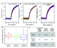
We fabricated zinc oxide (ZnO) TFTs using a zinc ammine complex with various zinc oxide sources such as ZnO, intrinsic Zn(OH)2, and precipitated Zn(OH)2. From the analyses of the reaction mechanism, surface morphology, crystal structure, and oxygen vacancy in the ZnO films, we confirmed the same intermediate in ZnO semiconductor films irrespective of the type of zinc oxide source in the zinc ammine complex precursor. The results showed the analogous value of the average field effect mobility, on/off current ratio, and turn-on voltage in all solution-processed ZnO TFTs. In conclusion, we confirmed that directly dissolving pristine ZnO into ammonia water is the most efficient method for preparing the ZnO semiconductor precursor, the zinc ammine complex, for low-temperature, solution-processed, and high performance ZnO TFTs.


Metal oxide semiconductors, such as indium (In), gallium (Ga), and zinc (Zn) oxides, are emerging as a strong substance for next generation display technology due to their unique properties, such as transparency, high electron mobility, and processability. Their distinctive electrical properties are caused by the conduction band minimum (CBM), which works as an electron pathway due to the s-orbital overlap when the principle quantum number is higher than 4.1 Since Nomura et al. successfully demonstrated the high performance n-type indium–gallium–zinc oxide (IGZO) thin film transistors (TFTs), the recent processes for metal oxide TFTs, such as vacuum sputtering, could ensure a high quality performance, good reproducibility, and reliability.2 While the sputtered IGZO TFTs have been built in commercialized organic light emitting diode (OLED) TVs, the vacuum process still has a challenging problem in the next generation display fabrication in terms of continuous processes, such as roll-to-roll processing. Consequently, solution-processed metal oxide semiconductors have been the focus of the effort to identify a low-cost continuous process. Moreover, they have shown a good potential for high performance and low-temperature process for flexible display devices.3–6

In general, the sol–gel method, which uses zinc acetate as precursors, is the most common method for solution-processed ZnO semiconductors; however, this method needs a high annealing temperature process causes serious restrictions in flexible device applications that use common plastic substrates.7 To overcome this limitation, Keszler et al. reported that ammine hydroxo zinc complex is a new precursor for the low temperature annealing process.8 In the fabrication of ZnO semiconductors, this precursor has several advantages: low temperature process, high electrical performance, and solution process. Other methods form preparing a zinc ammine complex using zinc hydroxide or zinc oxide powder as precursors for ZnO semiconductors were also reported.9–13 Although there are several approaches for using zinc ammine complex for ZnO semiconductors, no reports directly compare the performance of the ZnO semiconductors fabricated by different zinc oxide sources.

Herein, we respectively characterized the TFT performance of ZnO semiconductors fabricated by the zinc ammine complex made from three different zinc oxide sources. We also analysed the intermediate structure, oxygen vacancy, and crystal structure for ZnO semiconductors made from each of the zinc oxide sources using various instruments. In our comprehensive study, we found all the similar electrical properties in all ZnO TFTs fabricated by the three different zinc oxide sources, which were previously reported, and proved that the best way to prepare a zinc ammine complex for solution-processed ZnO semiconductor is the simple dissolution of pristine ZnO powder in ammonia water.

We prepared the zinc ammine complex for ZnO films with three zinc oxide sources. The first zinc oxide source was pristine ZnO powder (Sigma Aldrich, 99.999%). The second source was intrinsic Zn(OH)2 (Junsei, 98%). The third source was precipitated Zn(OH)2, according to the previously reported method by Keszler et al.8 All the zinc ammine complexes for a ZnO semiconductor were prepared by the dissolution of those three zinc oxide sources. Moreover, all the precursors were refrigerated for one day. Refrigerating the ZnO precursors enhances the solubility of the zinc oxide sources.14 The concentration of all the zinc ammine complexes were fixed at 90 mM for the comprehensive comparison of ZnO semiconductor performance under the same process conditions (see the ESI, Fig. S1). All prepared solutions were filtered through a hydrophilic 0.45 μm PTFE syringe filter and spin-coated with 3000 rpm for 30 s on substrates. After deposition, the ZnO films were annealed immediately on preheated hot plate at 300 °C for 1 h. Using these ZnO films, we fabricated the ZnO TFTs with bottom gate and top contact geometries to demonstrate the electrical performance of ZnO semiconductor films. Details about the experiments for ZnO TFTs fabrication were introduced in the ESI.

The amphoteric property of ZnO and the weak acidity of the Zn cation provide a wide range of solubility.14,15 Keszler et al. first reported the dissolution of Zn salts in ammonia water for a ZnO semiconductor precursor. Despite the good performance and process advantages, time-consuming and cumbersome processes for complex precipitation steps cause considerable deviations when preparing the precursor, which may induce large electrical performance variation in ZnO TFTs. To avoid the complicated precipitation reaction, Anthopoulos et al. and Moon et al. reported intrinsic zinc hydroxide as the zinc oxide source for a zinc ammine complex.9,10 However, as high purity zinc hydroxide products are not commercially available, the low purity of zinc hydroxide may degrade the ZnO semiconductor performance. Consequently, zinc hydroxide still has fundamental limitations, such as the complexity of the reaction or the unknown impurity of commercial products. Hence, directly dissolving ZnO powder in to ammonia water stands out as a promising zinc oxide source for a zinc ammine complex due to its one-step fabrication process and high purity level.12,13 However, there are no comprehensive studies for the structural and electrical properties of ZnO semiconductor films regarding the type of zinc oxide sources.

Scheme 1 shows the chemical reaction of a zinc ammine complex from different zinc oxide sources. Both zinc oxide and zinc hydroxide were transformed into a zinc ammine complex by aqueous ammonium ion. However, due to the high pH value (pH 11) of ammonia water, the zinc ammine complex was turned into an ammine–hydroxo zinc complex.16 In the previous papers, zinc intermediates were given various names, such as ammine–hydroxo zinc complex, sol precursor, or ZnO precursor solution. These unclear expressions created confusion about the intermediate. We referred to the zinc ammine complex as an intermediate for escaping confusion. The intermediate is important for low-temperature thermodynamics and the rapid kinetic of transformation to ZnO semiconductors.17,18 We investigated 1H-NMR (see the ESI, Fig. S2) spectra of various zinc ammine complexes and analysed them using deuterium dioxide to confirm the intermediate. The 1H-NMR data were obtained in ppm (δ) from the internal standard and chemical shift (multiplicity coupling constant in Hz, integration). The zinc ammine complex made from three zinc oxide sources showed only one peak as a singlet, as follows: ZnO powder δ = 1.16 (s, 4H); intrinsic Zn(OH)2 δ = 1.15 (s, 4H); precipitated Zn(OH)2 δ = 1.17 (s, 4H). We could speculate that the detected peaks around 1.16 ppm show the zinc ammine complex proton. From the analysis of the chemical reaction steps and the 1H-NMR spectra, we could conclude that the same intermediate was fabricated irrespective of zinc oxide sources for the zinc ammine complex. Although the zinc ammine complex for ZnO was prepared from different zinc oxide sources, it had the same ZnO intermediate in the chemical reaction. With these results, we could expect that the ZnO semiconductors fabricated from the zinc ammine complex show a similar performance irrespective of the different zinc oxide sources.


image file: c3ra47437b-s1.tif
Scheme 1 Reaction mechanism of ZnO made from a zinc ammine complex prepared with various zinc oxide sources: ZnO powder, intrinsic Zn(OH)2, precipitated Zn(OH)2.

To prove our speculation, we fabricated bottom gate top contact type ZnO TFTs. In Fig. 1, devices 1, 2, and 3 represent TFTs including the ZnO film fabricated with the zinc ammine complex prepared with ZnO powder, intrinsic Zn(OH)2, and precipitated Zn(OH)2, respectively. Fig. 1a–c shows the transfer curves of the ZnO TFTs that were fabricated with three zinc oxide sources, respectively. The field effect mobility was derived from the transfer curve at the saturation region. Device 1, 2, and 3 exhibited the average field effect mobility of 2.9 cm2 V−1 s, 2.5 cm2 V−1 s, and 2.6 cm2 V−1 s, respectively. The output curves of all the ZnO TFTs show n-type behaviour irrespective of zinc oxide source (see the ESI, Fig. S3). The other electrical properties of the ZnO TFTs prepared using three zinc oxide sources are shown in Fig. 1e. Considering the histogram data of the ZnO TFTs (see the ESI, Fig. S4), these results reveal that similar electrical properties were obtained. In addition, Fig. S5 shows that the hysteresis of the current between the forward and backward gate voltage sweep was negligible. A bias stress test (40 V, 6000 s) was also carried out and the curves of ΔVth vs. the bias time are shown in Fig. S6. All data show the analogous electrical properties.


image file: c3ra47437b-f1.tif
Fig. 1 (a)–(c) Transfer curves of ZnO TFTs made from a zinc ammine complex prepared with ZnO powder, intrinsic Zn(OH)2 and precipitated Zn(OH)2, respectively. (d) Average filed effect mobility of various ZnO TFTs. (e) Table of the electrical properties of various ZnO TFTs.

These results confirmed that the same chemical intermediates were brought out irrespective of the three different zinc oxide sources and the analogous electrical properties of the all ZnO TFTs were acquired. In this study, the three approaches used for fabricating a zinc ammine complex had the same chemical intermediates and showed a similar performance. The large deviation of mobility of device 3 was caused by the limitation of the precipitation method. In precipitated Zn(OH)2 for device 3, during the complex reaction process, each process could cause contamination resulting in considerable deviation in the step-by-step process. The complex and time-consuming processes for synthesis, precipitation, and removing residuals of precipitated Zn(OH)2, also made it difficult to maintain the uniformity of the process. The complexity may be the limitation of a zinc ammine complex made with precipitated Zn(OH)2. Fig. 2a–c shows the AFM images of the ZnO thin films in devices 1, 2 and 3. The root mean square (RMS) roughness of the ZnO thin film in devices 1, 2, and 3 were 0.387 nm, 0.326 nm, and 0.439 nm, respectively. As the change of the surface morphology in the ZnO films were too small, any strong correlating was not detected with the field effect mobility.19 In addition to surface morphology, the crystallinity of ZnO semiconductor also affects the electron transport in the active layer. With regard to binary oxides such as ZnO, they are easily transformed into a polycrystalline structure during a low temperature annealing process. The electron transport mechanism of polycrystalline semiconductors is dominant to the grain boundary effect. Since the hopping of electrons is hindered by the grain boundary, which acts as an energy barrier, the grain boundary scattering limits the carrier transport and reduces electron mobility.20 Fig. 2d–f show the high resolution transmission electron microscope (HRTEM) images of the crystal structure and grain boundary. The nano-crystalline structure of the ZnO semiconductors was observed and thickness of ZnO films was 8 nm, irrespective of zinc oxide source. Fig. S7 shows the fast Fourier transform selected area electron diffraction (FFT-SAED) patterns of each of the ZnO films. We could not observe any remarkable differences, such as lattice distortions or migrations in the all ZnO films based on different zinc oxide sources for the zinc ammine complex. Faint scattering was induced by the amorphous dielectric layer. These results revealed that the crystal structures, boundary, and morphology of ZnO films were similar irrespective of the type of zinc oxide sources.


image file: c3ra47437b-f2.tif
Fig. 2 AFM and cross-sectional HRTEM images of various ZnO films made from a zinc ammine complex prepared with various zinc oxide sources (ZnO powder, intrinsic Zn(OH)2, and precipitated Zn(OH)2) on the SiO2 substrate at the annealing temperature of 300 °C. (a)–(c) AFM image of various ZnO films. (d)–(f) HRTEM image of various ZnO films.

Also, the analysis of chemical composition, such as oxygen vacancy and zinc oxide bonding, has been conducted to investigate the conduction mechanism of ZnO semiconductors.21 In ZnO semiconductors, oxygen vacancies could be the major source of the free electron carriers; that is, oxygen vacancy affects the field effect mobility. For this reason, we carried out X-ray photoelectron spectroscopy (XPS) and analysed O 1s spectra in XPS. As shown in Fig. 3a–c, the experimental O 1s peak of each device was coherently fitted by three Gaussian components, centered at 529.9 eV (OA), 530.8 eV (OB), and 531.8 eV (OC), respectively. The peak at 529.9 eV could be assigned to an oxygen ion in the ZnO lattices (OA), and the peak at 530.8 eV denoted the oxygen vacancies in the ZnO lattices (OB). The peak at 531.8 eV (OC) could be assigned to the oxygen in hydroxide (–OH), which includes the absorbed oxygen on the surface of the ZnO films as –CO3, H2O, and O2.22 In general, a good ZnO semiconductor shows a proper ratio between oxygen deficiency and metal oxide lattice (or ZnO bonding). Although the obvious ratio between oxygen vacancy and metal oxide lattice is somewhat controversial, the variation of ratio gives a enough information of the uniformity of ZnO semiconductor quality.23 In our analyses, the ratio of integrated area oxygen vacancy and total area in the various ZnO semiconductor films was analogous (Fig. 3d).24


image file: c3ra47437b-f3.tif
Fig. 3 The O 1s XPS spectrum of various ZnO films made from a zinc ammine complex prepared with various zinc oxide sources, (a) ZnO, (b) intrinsic Zn(OH)2, (c) precipitated Zn(OH)2. (d) The ratio of integrated area oxygen vacancy and total area in the various ZnO semiconductor films.

We speculated that the same chemical intermediate was formed irrespective of the type of zinc oxide sources and the ZnO semiconductor made from the same chemical intermediate showed the analogous ratio of oxygen vacancy. Consequently, no difference was found in the performance of the solution-processed ZnO TFTs using the zinc ammine complex based on various zinc oxide sources. To avoid a time-consuming process, a large deviation of mobility, or the limitation of impurity, it is optimal to fabricate a zinc ammine complex for solution-processed ZnO TFTs by directly dissolving pure ZnO into ammonia water.

In summary, we fabricated the solution-processed ZnO TFTs using zinc ammine complexes, which were prepared using ZnO powder, intrinsic Zn(OH)2, and precipitated Zn(OH)2. From the analysis of the reaction mechanism in the zinc ammine complex, we deduced that the same chemical intermediate (zinc ammine complex) was made from three different zinc oxide sources. In the study of 1H-NMR, surface morphology by AFM, crystal structure by HRTEM, and oxygen vacancy by XPS in the ZnO films, we confirmed the same intermediate and ZnO semiconductor film fabrication irrespective of the type of zinc oxide source for the zinc ammine complex. Consequently, they induced the analogous values of the average field effect mobility, on/off current ratio, and turn-on voltage in all ZnO TFTs. Although zinc ammine complexes for ZnO semiconductors were prepared using three different zinc oxide sources, the chemical intermediate and electrical performance were the same. These solution-processed ZnO films from zinc ammine complexes have various advantages such as low temperature process, high electron mobility, and non-toxic aqueous solution. In conclusion, we confirmed that the direct dissolution of pristine ZnO into ammonia water is the most efficient method for the fabrication of a zinc ammine complexes for low-temperature, solution-processed, and high performance ZnO semiconductors in TFTs.

Acknowledgements

This work was supported by Basic Research Program (2011-0018113) and Center for Advanced Soft Electronics (2011-0031635) funded by NRF of Korea government. Also, we thank for the academy-industry collaboration program of LG Display.

Notes and references

  1. T. Kamiya, K. Nomura and H. Hosono, J. Disp. Technol., 2009, 5, 273–288 CrossRef CAS.
  2. K. Nomura, H. Ohta, A. Takagi, T. Kamiya, M. Hirano and H. Hosono, Nature, 2004, 432, 488–492 CrossRef CAS PubMed.
  3. K. Kim, S. Park, J. B. Seon, K. H. Lim, K. Char, K. Shin and Y. S. Kim, Adv. Funct. Mater., 2011, 21, 3546–3553 CrossRef CAS.
  4. D. M. Han, K. W. Ko, C. H. Han and Y. S. Kim, J. Mater. Chem. A, 2013, 1, 8529–8533 CAS.
  5. D. H. Lee, Y. J. Chang, G. S. Herman and C. H. Chang, Adv. Mater., 2007, 19, 843–847 CrossRef CAS.
  6. Y. J. Chang, D. H. Lee, G. S. Herman and C. H. Chang, Electrochem. Solid-State Lett., 2007, 10, H135–H138 CrossRef CAS PubMed.
  7. V. Zardetto, T. M. Brown, A. Reale and A. Di Carlo, J. Polym. Sci., Part B: Polym. Phys., 2011, 49, 638–648 CrossRef CAS.
  8. S. T. Meyers, J. T. Anderson, C. M. Hung, J. Thompson, J. F. Wager and D. A. Keszler, J. Am. Chem. Soc., 2008, 130, 17603–17609 CrossRef CAS PubMed.
  9. Y. H. Lin, H. Faber, K. Zhao, Q. Wang, A. Amassian, M. McLachlan and T. D. Anthopoulos, Adv. Mater., 2013, 25, 4340–4346 CrossRef CAS PubMed.
  10. K. Song, J. Noh, T. Jun, Y. Jung, H. Y. Kang and J. Moon, Adv. Mater., 2010, 22, 4308–4312 CrossRef CAS PubMed.
  11. R. Theissmann, S. Bubel, M. Sanlialp, C. Busch, G. Schierning and R. Schmechel, Thin Solid Films, 2011, 519, 5623–5628 CrossRef CAS PubMed.
  12. S. Y. Park, B. J. Kim, K. Kim, M. S. Kang, K. H. Lim, T. Il Lee, J. M. Myoung, H. K. Baik, J. H. Cho and Y. S. Kim, Adv. Mater., 2012, 24, 834–838 CrossRef CAS PubMed.
  13. S. H. Yu, B. J. Kim, M. S. Kang, S. H. Kim, J. H. Han, J. Y. Lee and J. H. Cho, ACS. Appl. Mater. Interfaces, 2013, 5, 9765–9769 CAS.
  14. J. J. Richardson and F. F. Lange, Cryst. Growth Des., 2009, 9, 2570–2575 CAS.
  15. R. M. Pasquarelli, C. J. Curtis, A. Miedaner, M. F. A. M. van Hest, R. P. O'Hayre and D. S. Ginley, Inorg. Chem., 2010, 49, 5424–5431 CrossRef CAS PubMed.
  16. B. Zhao, C. L. Wang, Y. W. Chen and H. L. Chen, Mater. Chem. Phys., 2010, 121, 1–5 CrossRef CAS PubMed.
  17. Y. Ka, E. Lee, S. Y. Park, J. Seo, D. G. Kwon, H. H. Lee, Y. Park, Y. S. Kim and C. Kim, Org. Electron., 2013, 14, 100–104 CrossRef CAS PubMed.
  18. K. Seong, K. Kim, S. Y. Park and Y. S. Kim, Chem. Commun., 2013, 49, 2783–2785 RSC.
  19. G. Adamopoulos, A. Bashir, S. Thomas, W. P. Gillin, S. Georgakopoulos, M. Shkunov, M. A. Baklar, N. Stingelin, R. C. Maher, L. F. Cohen, D. D. C. Bradley and T. D. Anthopoulos, Adv. Mater., 2010, 22, 4764–4769 CrossRef CAS PubMed.
  20. K. Ellmer, J. Phys.: D Appl. Phys., 2001, 34, 3097–3108 CrossRef CAS.
  21. K. H. Lim, K. Kim, S. Kim, S. Y. Park, H. Kim and Y. S. Kim, Adv. Mater., 2013, 25, 2994–3000 CrossRef CAS PubMed.
  22. P. T. Hsieh, Y. C. Chen, K. S. Kao and C. M. Wang, Appl. Phys. A: Mater. Sci. Process., 2008, 90, 317–321 CrossRef CAS.
  23. S. Jeong, Y. G. Ha, J. Moon, A. Facchetti and T. J. Marks, Adv. Mater., 2010, 22, 1346–1350 CrossRef CAS PubMed.
  24. K. Kim, S. Y. Park, K. H. Lim, C. Shin, J. M. Myoung and Y. S. Kim, J. Mater. Chem., 2012, 22, 23120–23128 RSC.

Footnotes

Electronic supplementary information (ESI) available: Solubility test, H-NMR, output characteristics, histogram, hysteresis, bias test, SAED patterns of HRTEM. See DOI: 10.1039/c3ra47437b
Equally contributed to this work.

This journal is © The Royal Society of Chemistry 2014