Tin oxide with a p–n heterojunction ensures both UV and visible light photocatalytic activity†
Arun Kumar
Sinha
a,
P. K.
Manna
b,
Mukul
Pradhan
a,
Chanchal
Mondal
a,
S. M.
Yusuf
b and
Tarasankar
Pal
*a
aDepartment of Chemistry, Indian Institute of Technology, Kharagpur, 721302, India. E-mail: tpal@chem.iitkgp.ernet.in
bSolid State Physics Division, Bhabha Atomic Research Centre, Mumbai, 400 085, India
First published on 11th October 2013
Abstract
Tuning of the tin oxide (SnO/SnO2) heterojunction (TOHJ) has been made possible by heating the as-prepared p-type SnO semiconductor in air in a controlled fashion. Thus a better photocatalytic activity for dye degradation under UV, visible as well as solar light irradiation was achieved. Multiple reflection of light and the TOHJ of SnO plates facilitate the photocatalysis reactions.
Semiconductors from metal oxides and sulfides have sufficient band-gap energies for promoting or catalyzing a wide range of photochemical reactions of environmental interest. Ga2O3, TiO2, ZnO, Fe3O4, etc.1 show photocatalytic degradation of dye molecules under irradiation by UV light. The solar spectrum contains ∼43% visible light and only ∼5% UV light. Thus most of the oxide materials make use of only an insignificant portion of the solar spectrum for traditional photocatalysis reactions. Many modifications of traditional photocatalysts have been reported for making them active under visible light. In all cases, a visible light absorbing material is attached to the traditional photocatalyst and then the electron–hole pair becomes separated.2–5 Lee et al. have designed a junction between p-type CaFe2O4 and n-type PbBi2Nb1.9W0.1O9, resulting in a highly active material for photocatalysis.6 Not only is a heterojunction between the p- and n-type semiconductors necessary, but also a junction between the two different phases of the same material is required for improved photocatalytic activity of a material, e.g. TiO2 with an anatase/rutile phase,7 Ga2O3 with an α/β phase,8etc.
We have discovered unusual photocatalytic activity of the as-prepared SnO under UV light as well as sunlight. This prompted us to examine the as-prepared tin oxide material and we found a thin SnO2 layer on the SnO, which was a natural tin oxide heterojunction (TOHJ) created spontaneously on the SnO plates. Furthermore, controlled heating in air in successive stages ensured the tuning of the SnO2 layer on SnO. The as-obtained materials were then tested individually for photocatalytic dye degradation. To the best of our knowledge, we, for the first time, report the photocatalytic activity of a SnO2-jacketed SnO material under irradiation by UV light as well as by visible light (Scheme 1).
 | ||
| Scheme 1 Schematic diagram for MB degradation on the tin oxide nanoplate, i.e. on the TOHJ surface, under sunlight irradiation. | ||
Pure SnCl2·2H2O powder reacted with NaOH solution to produce a blue black SnO material in gram quantity. The detailed reaction process is given in the ESI (ESI 1).† The optical properties of the SnO material were critically investigated. A broad absorption spectrum with peaks positioned at 253 nm and 500 nm was observed from the blue black SnO sample, which is shown in Fig. 1a. The theoretical expression for the determination of the band gap of a semiconductor material is given by the following equation:
| αEp = K(Ep − Eg)1/2 |
 | ||
| Fig. 1 UV-visible absorption spectra of SnO (a) and SnO2 (b) from diffuse reflectance spectroscopy and the corresponding band gap values of SnO (c) and SnO2 (d). | ||
Under ambient temperature, an ultra thin layer of SnO2 formed creating a TOHJ on the surface of SnO, which increased upon heat treatment. The SnO to SnO2 transformation was authenticated by DRS (diffuse reflectance spectroscopy) (ESI 2†).
The n-type SnO2 formed a stable and tunable heterojunction on the as-prepared p-type SnO semiconductor by heat treatment in steps, which was revealed from Rietveld refined analysis. The powder XRD and refined (using the FullProf program)10 X-ray diffraction patterns of the as-prepared and annealed (at different temperatures) SnO samples are shown in the ESI (ESI 3a and b).†
The as-prepared sample was found to be crystalline SnO with a layered tetragonal litharge-type structure with the space group P4/nmm. After annealing the as-prepared sample at 200 °C, a mixed phase containing 83.79 (0.29) weight% of SnO and 16.21 (0.35) weight% of SnO2 was obtained. At 400 °C, apart from an almost equal amount of the SnO and SnO2 phases, a third phase of Sn3O4 was also found in a small amount (∼2 weight%). At 800 °C, only the SnO2 phase was found in the sample, which crystallized in a tetragonal rutile-type structure with the space group P42/mnm. The structural data of SnO and SnO2 are given in the ESI (ESI 4).† In the Raman spectra of SnO, we identified two strong modes with frequencies at 113 cm−1 and 211 cm−1, which are in good agreement with the reported values.11 During the Raman analysis, a chemical transformation of the SnO surface occurred due to local heating by the laser light. The transformation from SnO to SnO2 in air passes through an intermediate form of Sn3O4, indicated by weak peaks between 100 and 200 cm−1 (Fig. 2a and b). The peak at 619.32 cm−1 is assigned to SnO2 formation (Fig. 2b) because of the local heating of the SnO samples by laser light,12 which is consistent with the peak at 638.62 cm−1 for a pure SnO2 sample (ESI 5†).
 | ||
| Fig. 2 Raman spectra of the SnO nanoplates with different laser powers (633 nm He–Ne laser with an acquisition time of 30 s) (a) and Raman spectra of the SnO nanoplates with different laser exposure times under 20 mW laser power (b). | ||
The intermediate phase was clearly identified as coexisting with SnO2 below 600 °C. The chemical transformation from SnO to SnO2 was also authenticated from TG and DTA analyses with a phase transition temperature of 561 °C (ESI 6†). At room temperature and above, the outer surface of SnO was subjected to air-oxidation, forming SnO2, which was confirmed by XPS analysis. The transformation of SnO to SnO2 was spontaneous in air and this is supported by the standard Gibbs energy of formation.13 Regarding the oxidized SnO2 layer, the dominant signals corresponding to Sn 3d5/2 and Sn 3d3/2 were found at 486.6 eV and 495.0 eV (ESI 7†), matching very well with those reported for SnO2.14 It has been reported in the literature that for pure SnO (non-hygroscopic), tin has a binding energy at 485.6 eV (Sn 3d5/2) and 494.0 eV (Sn 3d3/2).13 As for O 1s, the peak at 529.7 eV was assigned as O in SnO and the peak at 530.4 eV was assigned as O in SnO2. Additionally, the extra peak for O 1s at 531.9 eV was indexed to –OH groups, which is thought to stem from the hydrated structure of SnO2 (ESI 7†). This is also supported by FTIR analysis (ESI 8†). Fig. 3a and b are FESEM images showing the morphology of the products in different magnifications. The most interesting result is that the product has a plate type morphology for which the BET surface area is given in the ESI (ESI 9).† The typical length of the nanoplates was 2–5 μm with 200–400 nm thickness. Representative HRTEM images (Fig. 3e and f) revealed that the SnO nanoplates were crystalline with clear lattice fringes parallel to the walls. The values for the central and edge parts were 0.244 nm and 0.240 nm, respectively. The inter-planar distance was 0.240 ± 0.004 nm for the (001) plane, perpendicular to the growth axis and could readily be resolved for the tetragonal phase of the SnO nanocrystals. A clear HRTEM image of SnO–SnO2 with the p–n heterojunction is shown in the ESI (ESI 10).† Polycrystalline SnO2 was deposited on the surface of SnO and the inter-planar distance was 0.337 ± 0.002 nm for the (110) plane of SnO2. Due to the solid state chemical reaction, the SnO nanoplates were gradually deformed from their original shape by rapid oxidation at elevated temperature as shown in the ESI (ESI 11).†
 | ||
| Fig. 3 FESEM images of SnO nanoplate at low (a), high (b) magnification, TEM images of SnO nanoplate at low (c), medium (d) magnification, HRTEM image of the central part (e), edge part (f) of the nanocrystal, SAED pattern at the central part (g) and edge (h) of the SnO nanocrystal. | ||
Photocatalytic reactions on the surface of the SnO nanoplates occurred under sunlight or artificial visible/UV-light illumination (the detailed procedure for the photocatalysis reaction is given in ESI 12†). ESI 13† represents the photocatalytic decolorization of MB in the presence of artificial UV and visible light. The time dependent UV-visible absorption spectra of the dye degradation are shown in the ESI (ESI 13a and b).† Interestingly, the degradation of MB under UV and visible light was quite different, which was confirmed from the UV-visible data. The aqueous solution of MB photocatalytically degraded completely overnight under UV irradiation. This was confirmed by the gradual diminution and the blue shifting of the λmax of the original 662 nm peak of the dye.15 However, under visible light, the absorption peak at 662 nm decreased gradually and disappeared overnight without any shift in the peak position. This means that there was no photooxidative N-demethylation of MB but a direct cleavage of the aromatic ring of the dye molecule in water by active oxygen and radical species as a result of the photogenerated electrons and holes.16 Again, the photocatalysis reaction depended on the intensity of the light. We performed comparative dye degradation experiments with different light sources: W-lamp for 200 W and 500 W visible light, and solar light. The results (shown in Fig. 4a and ESI 14†) clearly show that solar light had the highest efficiency over artificially created visible light. The SnO sample was annealed at four different temperatures: 200 °C, 400 °C, 600 °C, and 800 °C.
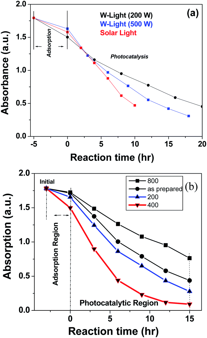 | ||
| Fig. 4 Comparison of the photocatalytic degradation of MB in the presence of the tin oxide nanoplates under different wattage values (a) and comparison of the photocatalytic degradation of MB in the presence of annealed tin oxide samples under UV-light (365 nm) (b). | ||
Each sample was then employed separately for the photodegradation of MB (ESI 15†). A comparison of the MB degradations is shown in Fig. 4b. Amongst the four annealed samples, the SnO sample obtained from annealing at 400 °C showed the best photocatalytic activity compared to any other. The annealed products contained a mixture of varying compositions and displayed unexpectedly high photocatalytic activities.
The photocatalytic activity of the material depended on the material composition and the active surface area.
The BET surface areas of the annealed SnO samples are shown in the ESI (ESI 16).† There are significant small changes in the BET surface areas of the different annealed SnO samples.
The n-type semiconductor SnO2 encased the as-prepared p-type semiconductor SnO and formed a tin oxide heterojunction (TOHJ). The results authenticate the tuning of the p–n heterojunction by heat treatment to make the composite useful and efficient for photocatalytic reactions. The band diagram with the charge separation of the SnO–SnO2 (p–n) heterojunction is shown in Fig. 5. In the band diagram, the VB positions of SnO and SnO2 were obtained from the XPS results (ESI 17†), which are slightly shifted from the literature values,17 and the CB positions were determined from DRS with the Tauc plots, and thus the band gap was ascertained. However, prolonged heating quantitatively transformed SnO into SnO2 and finally the TOHJ disappeared. The resultant effect was the loss of visible light photocatalytic activity due to the complete disappearance of the heterojunction. The nanoplate structure allowed a more efficient transport of the reactant molecules, allowing them to come into contact with the active sites on the nanoplate framework. Moreover, the nanoplates may allow multiple reflections of light by the planar surface of SnO, which presumably facilitates a more efficient use of the light source, hence the efficiency of the photocatalysis reaction is enhanced. Experiments have also showed that the SnO nanoplates could be readily separated from the reaction mixture by filtration or decantation after the photocatalytic reaction. The catalyst retained its original photocatalytic activity and morphology even after four repeated cycles of the photodegradation experiment, confirming the robustness of the SnO nanoplates.
 | ||
| Fig. 5 Band diagram of the SnO–SnO2 (p–n) heterojunction and the charge separation, i.e. the electron and hole separation, under light irradiation. | ||
Acknowledgements
We are thankful to CSIR, UGC, DST, New Delhi and I.I.T Kharagpur, India. We are also thankful to Prof. Kumar Biradha for providing us the facility for the BET surface area measurements.Notes and references
- M. R. Hoffmann, S. T. Martin, W. Choi and D. W. Bahnemannt, Chem. Rev., 1995, 95, 69 CrossRef CAS.
- G. Shengli, D. Qingzhang and J. Yu, J. Environ. Sci. Technol., 2009, 43, 7079 CrossRef.
- C. Hu, X. Hu, L. Wang, J. Qu and A. Wang, Environ. Sci. Technol., 2006, 40, 7903 CrossRef CAS.
- Y. G. Zhang, L. Lima, J. L. Li and Y. Yu, Environ. Sci. Technol., 2007, 41, 6264 CrossRef CAS.
- H. Yu, X. Li, X. Quan, S. Chen and Y. Zhang, Environ. Sci. Technol., 2009, 43, 7849 CrossRef CAS PubMed.
- H. G. Kim, P. H. Borse, W. Choi and J. S. Lee, Angew. Chem., Int. Ed., 2005, 44, 4585 CrossRef CAS PubMed.
- T. Kawahara, Y. Konishi, H. Tada, N. Tohge, J. Nishii and S. Ito, Angew. Chem., Int. Ed., 2002, 41, 2811 CrossRef CAS.
- X. Wang, Q. Xu, M. Li, S. Shen, X. Wang, Y. Wang, Z. Feng, J. Shi, H. Han and C. Li, Angew. Chem., Int. Ed., 2012, 51, 13089 CrossRef CAS PubMed.
- J. Tauc, Mater. Res. Bull., 1968, 3, 37 CrossRef CAS.
- J. R. Carvajal, Commission on Powder Diffraction (IUCr) Newsletter, 2001, 12, 26.
- J. Geurts, S. Rau, W. Richter and F. J. Schmitte, Thin Solid Films, 1984, 121, 217 CrossRef CAS.
- F. Buciuman, F. Patcas, R. Craciun and D. R. T. Zahn, Phys. Chem. Chem. Phys., 1999, 1, 185 RSC.
- L. Y. Liang, Z. M. Liu, H. T. Cao and X. Q. Pan, ACS Appl. Mater. Interfaces, 2010, 2, 1060 CAS.
- Y. C. Her, J. Y. Wu, Y. R. Lin and S. Y. Tsai, Appl. Phys. Lett., 2006, 89, 043115 CrossRef.
- T. Zhang, T. Oyama, A. Aoshima, H. Hidaka, J. Zhaob and N. Serpone, J. Photochem. Photobiol., A, 2001, 140, 163 CrossRef CAS.
- G. Lui and J. Zhao, New J. Chem., 2000, 24, 411 RSC.
- Y. Xu and M. A. A. Schoonen, Am. Mineral., 2000, 85, 543 CAS.
Footnote |
| † Electronic supplementary information (ESI) available: Materials, instruments, preparation of the SnO nanoplates, DR spectra and powder XRD data of the as prepared and different heat treated SnO nanocrystals, Rietveld refined XRD patterns, structural data for the SnO and SnO2 materials from the Rietveld analysis, Raman spectra of the heat treated SnO nanoplates, thermal analysis, XPS analysis of the SnO nanoplates, FTIR spectra of the powder SnO, nitrogen adsorption–desorption isotherms of the SnO nanoplates and the annealed SnO, morphology of the SnO nanoplates at different temperatures, photodegradation experiments, photocatalytic degradation of MB, and VB position determination from the XPS spectra. See DOI: 10.1039/c3ra42740d |
| This journal is © The Royal Society of Chemistry 2014 |