Hexagonal ZnO/SnO2 core–shell micropyramids: epitaxial growth-based synthesis, chemical conversion, and cathodoluminescence
Qin
Kuang
*a,
Xi
Zhou
b and
Lan-Sun
Zheng
a
aDepartment of Chemistry, College of Chemistry and Chemical Engineering, Xiamen University, Xiamen 361005, P.R. China. E-mail: qkuang@xmu.edu.cn; Tel: +86 592 2187879
bDepartment of Biomaterials, College of Material Science, Research Center of Biomedical Engineering Technology of Xiamen City, Xiamen University, Xiamen, 361005, P.R. China
First published on 24th January 2014
Abstract
In this paper, ZnO/SnO2 core–shell micropyramids were successfully prepared via a chemical vapor deposition process that is based on the epitaxial growth of SnO2 on the surface of ZnO hexagonal micropyramids. Upon controlling appropriate deposition times and flow rates of the precursor, two epitaxial growth modes of SnO2, i.e. a continuous thick film and well-arranged one-dimensional nanostructures were observed in the ZnO/SnO2 core–shell micropyramids. Taking advantages of the difference in acid resistance between ZnO and SnO2, the as-prepared ZnO/SnO2 micropyramids were further converted into SnO2 hollow micropyramids with a facile acid-etching treatment. Structural analysis revealed that the lattice mismatch degree between epitaxial planes determines the preferential growth direction of the SnO2 epitaxial layer on the ZnO surface. Compared to the pristine ZnO template, interestingly, the ZnO/SnO2 core–shell micropyramids exhibited very strong green emission around 504 nm. Such enhanced green emission should be induced by high-density structural defects generated in the interfacial area during the epitaxial growth.
1. Introduction
In the past decade, various functional heterostructures, including core–shell heterostructures, co-axial, bi-axial or tri-axial heterostructures, segmented heterostructures, and hierarchical heterostructures, have attracted increasing attention due to their unique properties and multifunctional applications.1–8 Theoretically, what form of morphology the heterostructures are adopted in first depends on the crystallographic compatibility between the secondary material and the parent material, especially in atomic arrangement and lattice matching degree at the hetero-interface. In this regard, it is quite understandable why most heterostructures with a well-crystallized epitaxial interface are usually grown with two materials possessing the same or similar crystal structures.1,6,9–11 As for those materials with different crystallographic structures, it is a great challenge to acquire desirable heterostructures with epitaxial interfaces, which relies on comprehensive understanding of crystallographic structural features of materials as well as precise controlling of synthetic conditions.ZnO and SnO2 are two important functional materials and widely used in catalysis, gas sensing, solar cells, light-emitting devices, etc. In the past years, many efforts have been devoted into the syntheses of ZnO and SnO2 composite heterostructures due to possible multifunctional applications from synergistic effects.12,13 Structurally, ZnO and SnO2 belong to the hexagonal wurtzite-type structure and tetragonal rutile-type structure, respectively. The apparent structural difference between wurtzite-type and rutile-type structures seems so large that the epitaxial ZnO–SnO2 heterostructures are seldom reported. Recently, the fabrication of ZnO/SnO2 core–shell tetrapods with an epitaxial interface was successfully realized on the basis of the comparability of atom arrangement between the ZnO-(01![[1 with combining macron]](https://www.rsc.org/images/entities/char_0031_0304.gif) 0) plane and the SnO2-(100) plane.14 Subsequently, other ZnO/SnO2 epitaxial heterostructures including SnO2/ZnO core–shell nanobelts or nanowires,15,16 SnO2/ZnO/SnO2 triaxial nanobelts,17 and ZnO/SnO2 or SnO2/ZnO hierarchical heterostructures,18,19 and were reported in succession. Although some growth mechanisms have been proposed,14,17,19 the epitaxial relation between ZnO and SnO2 is still lacking a comprehensive understanding. Hence it is necessary to thoroughly investigate the epitaxial growth of ZnO–SnO2 on different specific crystal surfaces and probe the relaxation mechanism of the lattice mismatch strain.
0) plane and the SnO2-(100) plane.14 Subsequently, other ZnO/SnO2 epitaxial heterostructures including SnO2/ZnO core–shell nanobelts or nanowires,15,16 SnO2/ZnO/SnO2 triaxial nanobelts,17 and ZnO/SnO2 or SnO2/ZnO hierarchical heterostructures,18,19 and were reported in succession. Although some growth mechanisms have been proposed,14,17,19 the epitaxial relation between ZnO and SnO2 is still lacking a comprehensive understanding. Hence it is necessary to thoroughly investigate the epitaxial growth of ZnO–SnO2 on different specific crystal surfaces and probe the relaxation mechanism of the lattice mismatch strain.
In this paper, hexagonal ZnO micropyramids were used as templates to provide two kinds of typical ZnO crystal planes (i.e., {0001} and {011}) for the epitaxial growth of SnO2 during the chemical vapor deposition (CVD). Upon controlling appropriate deposition times and flow rates of the precursor, two epitaxial growth modes of SnO2, i.e. a continuous thick film and well-arranged one-dimensional nanostructures were observed in the ZnO/SnO2 core–shell micropyramids. Furthermore, SnO2 hollow micropyramids were successfully obtained with a facile acid-etching treatment on the as-prepared ZnO/SnO2 core–shell micropyramids. Based on careful microscopy observation and structural analysis, it is found that the SnO2 epitaxial film prefers to grow along the minimum lattice mismatch direction (i.e., [20]ZnO//[001]SnO2) under the inductive effect of the lattice mismatch strain. Different from the pristine ZnO micropyramids, the as-prepared ZnO/SnO2 core–shell micropyramids exhibited a strong green luminescence, which is associated with the high-density structural defects in the interfacial area during the epitaxial growth process.
2. Experimental section
2.1 Synthesis of ZnO hexagonal micropyramids
ZnO hexagonal micropyramids were fabricated according to our previous study.20 In a typical experiment, 6.6 mL of oleic acid and 4.5 mL of ethylenediamine were mixed under stirring to form an orange liquid at room temperature, and then 1.46 g anhydrous zinc acetate was added. The resulting mixture was transferred into a long tube with one end closed, and rapidly heated to 286 °C for the thermo-decomposition of zinc acetate to ZnO. After reaction for 1 h, some white precipitates were collected and washed with hexane and ethanol several times. All the reagents were purchased from commercial sources (analytical grade) and used without further purification.2.2 Syntheses of ZnO/SnO2 core–shell micropyramids and SnO2 hollow micropyramids
The epitaxial growth of SnO2 on ZnO micropyramids was carried out in a homemade CVD apparatus, in which a direct current of 2–4.5 A passed through a n-Si (100) substrate (2 cm × 0.5 cm) loaded with some ZnO micropyramid powders so as to provide a high temperature of 500–850 °C for the samples deposited on the substrate.14 In a typical experiment, the ZnO hexagonal micropyramids were ultrasonically dispersed into anhydrous ethanol, and then dropped on the Si substrate. After the reaction chamber was vacuumed, the Si substrate loaded with ZnO micropyramids was heated to 770 °C by setting the current 4.5 A, and then a freshly prepared 8% SnH4–N2 mixed gas was introduced into the chamber, which would decompose into SnO2 (SnH4 + O2 → SnO2 + H2O) at the heating Si substrate. To control the growth of SnO2 on the ZnO micropyramids, the flow rates of SnH4–N2 were regulated in 10–30 standard cubic centimetres per minute (sccm), and the deposition procedure lasted for 30–180 s.The hollow SnO2 micropyramids were prepared via an acid-etching treatment on the ZnO/SnO2 core–shell micropyramids to remove the ZnO core. Typically, the Si substrates with the ZnO/SnO2 composite structures loaded were immersed in 0.1 M HCl solution for 30 min–2 hours, and then in distilled water without disturbance for more than 2 hours. The product was carefully collected from the substrate via ultrasonic agitation and centrifugation, and finally dried at 60 °C.
2.3 Characterization of samples
The morphology and structure of the products were characterized by powder X-ray diffraction (XRD, Panalytical X'pert), field emission scanning electron microscopy (FE-SEM, LEO 1530) equipped with energy dispersion spectroscopy (EDS), and high-resolution TEM (HRTEM, Philips TECNAI F-30). The room-temperature cathodoluminescence (CL) spectra and images of the samples were taken using a CL system (Gatan, MonoCL) equipped on a LEO1530 SEM.3. Results and discussion
3.1 Morphology and structure characterization of hexagonal ZnO/SnO2 micropyramids
Structurally, all surfaces of a hexagonal pyramidal ZnO crystal are enclosed by polar facets: the side surfaces are exposed with {011} planes and the bottom/top surfaces are bound with the O2−-terminated (000)/Zn2+-terminated (0001) planes, respectively.20 The typical morphology of the ZnO hexagonal micropyramids is shown in Fig. 1a. The corresponding XRD pattern (Fig. 1b) of the ZnO micropyramids confirms that the ZnO hexagonal micropyramids possess a hexagonal wurtzite structure (JCPDS no. 36-1451).
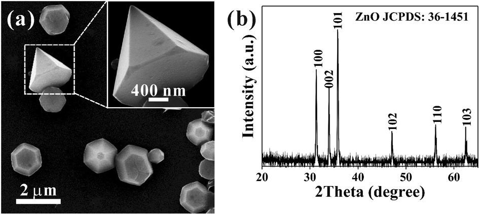 | ||
| Fig. 1 (a) SEM image and (b) XRD pattern of hexagonal ZnO micropyramids synthesized by thermal decomposition of anhydrous zinc acetate in the mixed solvent of oleic acid and ethylenediamine at 286 °C. | ||
The growth of SnO2 on specific faces of ZnO micropyramids were achieved through a CVD route, using a SnH4–N2 mixed gas as the precursor. Note that the flow rate of the precursor gas (SnH4–N2) and the deposition time are two crucial factors for the epitaxial growth of ZnO/SnO2 core–shell micropyramids. Fig. 2 show a series of typical SEM images of SnO2-deposited ZnO micropyramids, clearly depicting the epitaxial growth process of SnO2 on the surfaces of ZnO micropyramids at different deposition times (x-axis) and flow rates (y-axis). From these images, it can be seen that the growth of SnO2 on the ZnO hexagonal pyramid surfaces can be classified into three typical modes, i.e. nanoparticles, one-dimensional (1D) nanostructures like wires, and continuous thick film, which is for convenience denoted as ZnO/SnO2-P (particles), ZnO/SnO2-W (wires) and ZnO/SnO2-F (film), respectively. When the deposition time is very short (30 s), some SnO2 nanoparticles of several nanometers are grown on the surfaces of ZnO hexagonal micropyramids; as a result, the surfaces of the micropyramids look rough (Fig. 2a). With the deposition process proceeding, those tiny nanoparticles gradually grow along the same direction into some 1D nanostructures like wires, which cover the whole side and top/bottom surfaces of ZnO micropyramids in the form of tightly-arranged nanowires (Fig. 2b). On the other hand, the flow rate of SnH4–N2 greatly influences the continuity and the thickness of the SnO2 epitaxial layer. With the increase of flow rate, well-arranged nanowires disappear, while continuous SnO2 films gradually are generated (Fig. 2c).
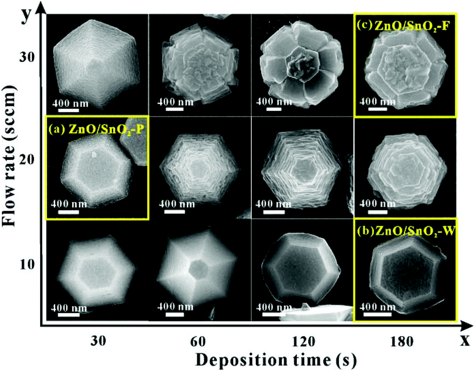 | ||
| Fig. 2 SEM images of ZnO hexagonal micropyramids after the SnO2 deposition at different times (x-axis) and flow rates (y-axis), clearly depicting the growth of SnO2 on different surfaces of ZnO micropyramids. Highlighted are three typical samples: (a) ZnO/SnO2-P (30 s, 20 sccm), (b) ZnO/SnO2-W (180 s, 10 sccm) and (c) ZnO/SnO2-F (180 s, 30 sccm). | ||
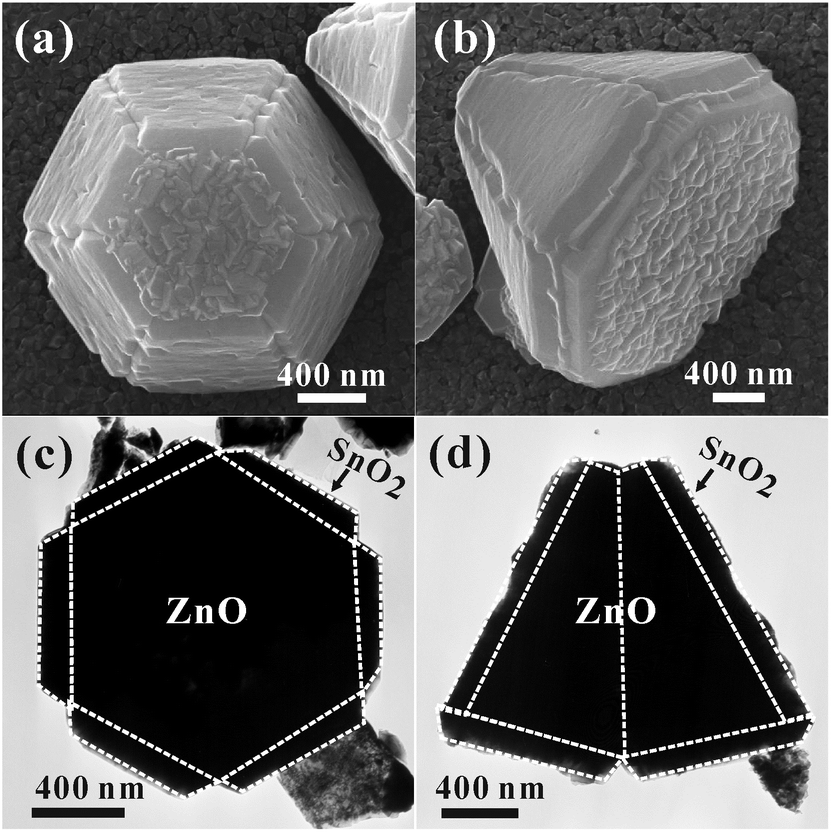
In order to make clear the growth relationship between the grown SnO2 layer and the ZnO template, more detailed electron microscopy characterizations were made on the as-prepared ZnO/SnO2-W and ZnO/SnO2-F core–shell micropyramids. In Fig. 3a are typical SEM images of the ZnO/SnO2-W micropyramids synthesized at a low flow rate (10 sccm) for 180 s, which clearly shows the growth status of the SnO2 shell on the different surfaces of ZnO micropyramids. From the high-magnification SEM image in Fig. 3b, it can be found that the deposited SnO2 layer on the side surfaces (i.e., {011}ZnO planes) is constructed with tightly arranged wire-like SnO2 nanostructures side by side. The diameters of these SnO2 nanowires are very uniform, about 15 nm, while the lengths vary from 50–1000 nm. Besides that, six grooves can be observed at the ridges of ZnO micropyramids. Interestingly, some special self-assembled patterns constructed with rod-like SnO2 nanostructures are observed on the top/bottom surfaces (i.e., {0001}ZnO planes) of ZnO micropyramids, as shown in Fig. 3c,d. In the growth direction, all SnO2 nanorods are parallel to the edges of the hexagonal horizontal section of micropyramids, i.e. along [20]. Note that the composition of the deposited wire-like nanostructures was well identified by EDS and XRD, where SnO2 is detected in addition to ZnO (Fig. 3e,f). The above results suggest that the growth of SnO2 follows a directed and preferential mode on both the {011}ZnO and {0001} facets of ZnO hexagonal micropyramids.
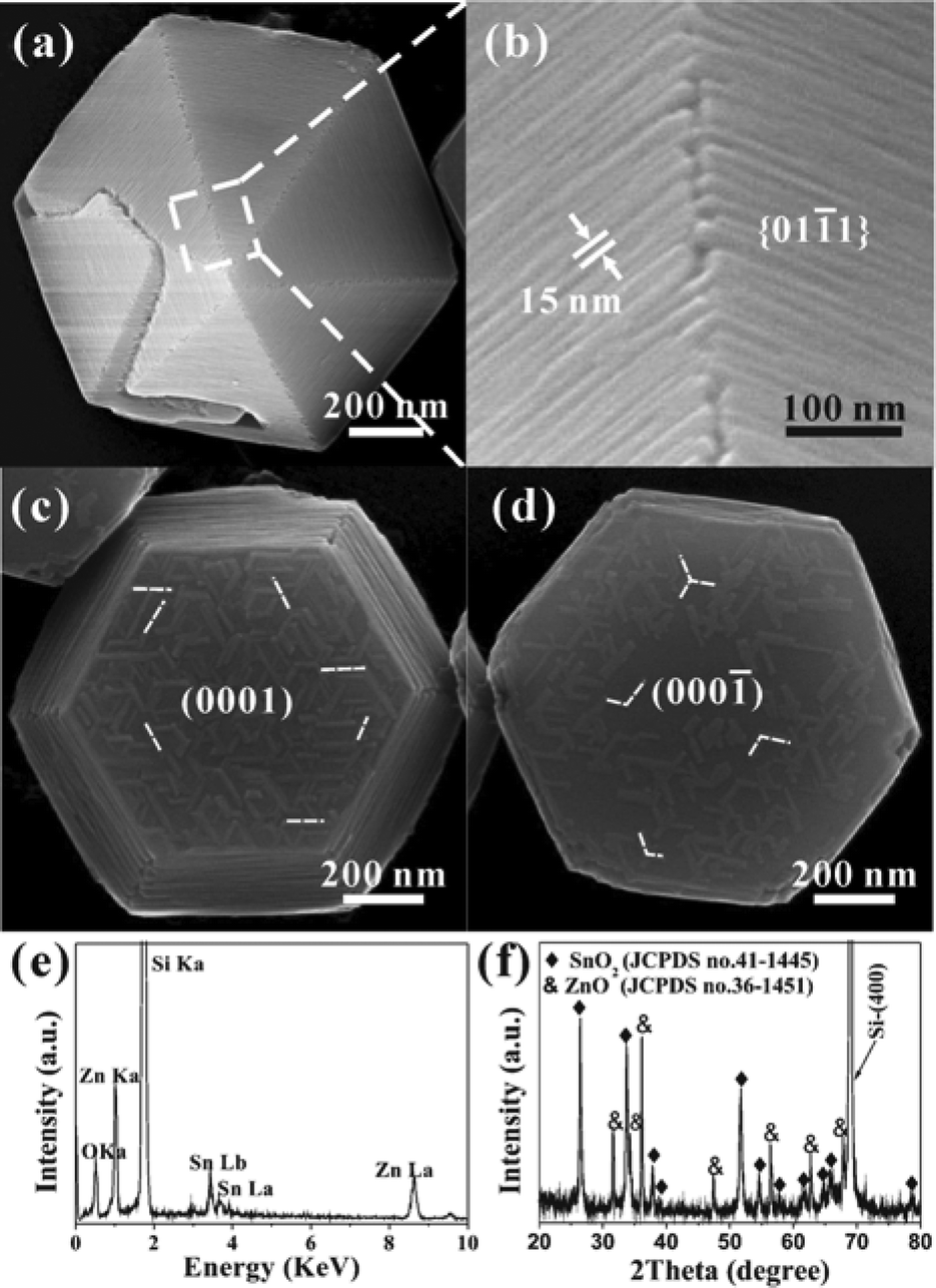 | ||
| Fig. 3 SEM images of different views on hexagonal ZnO/SnO2-W micropyramids synthesized at a deposition time of 180 s and a flow rate of 10 sccm: (a,b) SnO2 on the side surfaces (i.e., {011} faces) of a hexagonal ZnO micropyramid; (c,d) SnO2 on the top/bottom surfaces (i.e., ±(0001) faces) of a truncated hexagonal ZnO micropyramid. (e) EDS spectrum and (f) XRD pattern of the ZnO/SnO2-W micropyramids. | ||
More intrinsic structural information was revealed by TEM characterization. Fig. 4a is a low-magnification TEM image of a ZnO/SnO2 micropyramid, clearly showing the core–shell structural characteristics. In addition, a sharp interface is observed between the well-crystallized SnO2 shell and the ZnO template, and the thickness of the SnO2 shell is about 15 nm. The high-resolution TEM (HRTEM) image (Fig. 4b) shows that the spacing between adjacent planes is close to 0.268 nm, corresponding to the (101) planes of rutile SnO2. According to the fast Fourier transform (FFT) pattern (Fig. 4c) of the lattice, it can be seen that the epitaxial SnO2 shell grows along the [001]SnO2 direction on the side surfaces (i.e., {011}ZnO planes) of the ZnO micropyramid. Noticeably, the corresponding SAED pattern (inset in Fig. 4d) recorded from the whole core–shell micropyramid reveals that some satellite diffraction spots regularly appear around the diffraction spots (marked by arrows) assigned to hexagonal wurtzite ZnO. Those additional diffraction spots should be produced from the epitaxial SnO2 shell. As demonstrated in the previous study,14 there is little difference in growth orientation between the SnO2 films on the six side surfaces of the ZnO template. For this reason, the diffraction spots assigned to SnO2 are split, as shown in Fig. 4d. From the above results, it can be concluded that the growth of SnO2 on the side surfaces (i.e., {011}ZnO planes) of ZnO micropyramids follows the epitaxial relation: [20]ZnO//[001]SnO2 and [0001]ZnO//[100]SnO2, which is same as that on {010}ZnO planes reported in our previous study.14
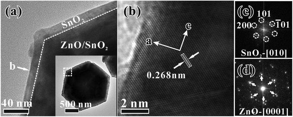 | ||
| Fig. 4 (a) Low-magnification TEM image recorded from one corner of a single ZnO/SnO2-W hexagonal micropyramid (inset) synthesized at a deposition time of 180 s and a flow rate of 10 sccm. (b) HRTEM image and (c) corresponding FFT pattern recorded from the side ‘b’ of the sample. (d) The SAED pattern recorded from the whole ZnO/SnO2-W hexagonal micropyramid. | ||
More detailed structural information about the ZnO/SnO2-F core–shell micropyramids is presented in Fig. 5. As shown in Fig. 5a,b, at higher flow rates (30 sccm) and longer deposition time (120 s and 180 s), a layer of thick and continuous SnO2 film is formed on every side surface of ZnO hexagonal micropyramids. Compared to the ZnO/SnO2-W core–shell micropyramids, the side surfaces of the ZnO/SnO2-F core–shell micropyramids are comparatively smooth. In TEM observations, such ZnO/SnO2-F core–shell micropyramids look like flowers with six petals (Fig. 5c,d). The thickness of the grown SnO2 film is in the range of 100–200 nm. Note that the SnO2 films are cracked near the ridges of ZnO hexagonal micropyramids, indicating that the epitaxial growth of SnO2 shell stops there.
 | ||
| Fig. 5 Top-view and side-view (a,b) SEM and (c,d) TEM images of flower-like ZnO/SnO2-F micropyramids obtained at 30 sccm flow rate and 180 s deposition time. | ||
3.2 Morphology and structure characterization of hollow SnO2 micropyramids
Since there is a large difference between ZnO and SnO2 in acid resistance, it is facile to convert the ZnO/SnO2 core–shell heterostructures into corresponding SnO2 hollow structures by sacrificially etching the ZnO core with acid treatment.14,21Fig. 6a,b show typical SEM and TEM images of as-prepared SnO2 hollow micropyramids via the etching treatment on the ZnO/SnO2-W micropyramids with 0.1 M HCl solution for 30 min. Without the support of the ZnO inner core, the pyramidal structure can be still retained, and the well-arranged SnO2 1D nanowires are still observed. The HRTEM image (Fig. 6c) taken from a side (the zone ‘c’) of a hollow micropyramid indicates that SnO2 nanowires indeed grow along the [001] direction, which is consistent with the results observed from the ZnO/SnO2-W micropyramids. The HRTEM image (Fig. 6d) taken from the bottom (the zone ‘d’) of hollow micropyramid indicates that the bottom seems a continuous film possessing periodical contrast fluctuation, instead of well-separated nanowires. From the inverse FFT image (Fig. 6e) of the zone ‘e’ of the bottom, the atomic arrangement on the bottom surface is consistent with that on the (010) plane of SnO2 shown in Fig. 6f. Since the ZnO core has been removed, the observed periodical contrast fluctuation is probably ascribed to the lattice mismatch strain accumulated in the SnO2 epitaxial shell, rather than the so-called Moiré pattern that usually results from the overlapping of different crystal lattices.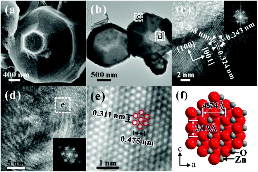 | ||
| Fig. 6 (a) SEM and (b) TEM images of the SnO2 hollow micropyramids converted from ZnO/SnO2-W micropyramids via an etching treatment with 0.1 M HCl for 30 min; (c,d) HRTEM images taken from the side (zone c) and the bottom (zone d) of a single hollow SnO2 pyramid. Insets are corresponding FFT patterns. (e) Inverse FFT image of the zone ‘e’ in (d); (f) schematic atom arrangement model of (010)SnO2 epitaxial plane. | ||
Through a similar acid-etching process, the flower-like ZnO/SnO2-F micropyramids can be also successfully converted into the corresponding SnO2 hollow nanostructures. Fig. 7a–c show typical morphologies of the as-acquired SnO2 hollow micropyramids in different orientations, which keep a similar flower-like shape to the micropyramids with the initial ZnO/SnO2-F template. Interestingly, the surface of the SnO2 shell become rough, and some 1D structures like ridges along the [20]ZnO direction are observed. These ridge-like SnO2 structures should result from strain-induced shrinking of the SnO2 film when not supported by the ZnO cores. The EDS spectrum (Fig. 7d) confirms that the ZnO cores have been completely removed via the etching treatment. According to the corresponding TEM image (Fig. 7e), the shell of SnO2 hollow micropyramids is completely closed, but there are some cracks in the shell, which provide the channels for acid etching.
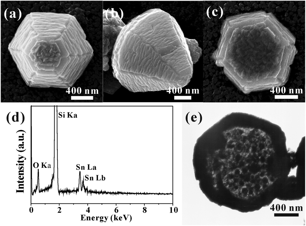 | ||
| Fig. 7 (a–c) Typical SEM images and (d) corresponding EDS spectrum of the SnO2 hollow micropyramids converted from ZnO/SnO2-F micropyramids via an etching treatment with 0.1 M HCl solution for 2 hours; (e) TEM image of a single SnO2 hollow micropyramid. | ||
3.3 Discussion about epitaxial growth mechanism of SnO2 on the surface of hexagonal ZnO micropyramids
The epitaxial growth has been demonstrated to take place between specific crystal planes of wurtzite-type ZnO and rutile-type SnO2, thereby producing various core–shell or hierarchical ZnO–SnO2 structures.14–19 In our previous study, the epitaxial growth of SnO2 on the {010}ZnO planes was primarily discussed, based on the structural compatibility of atomic stacking modes between in the ZnO-[0001] direction and in the SnO2-[100] direction.14 In fact, this structural characteristic is also responsible for the epitaxial growth of SnO2 on the {011} and {0001} planes of ZnO. As shown in Fig. 8a,b, the structural compatibility of atomic arrangements exists on the (010)SnO2//(010)ZnO and (100)SnO2//(0001)ZnO epitaxial planes, which makes it reasonable to epitaxially grow SnO2 on the side and bottom/top surface of ZnO micropyramids.
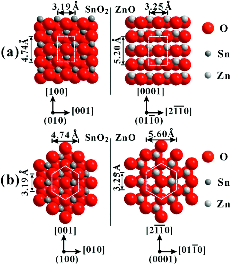 | ||
| Fig. 8 Schematic models of the atomic arrangements (a) on the epitaxial (010)SnO2//(010)ZnO planes, and (b) on the epitaxial (100)SnO2//(0001)ZnO planes. | ||
As found in the ZnO/SnO2-W micropyramids, on both {011} and {0001} planes of ZnO, SnO2 is able to form well-arranged 1D nanostructure patterns. This phenomenon is very interesting, which is associated with the difference of lattice mismatch in different growth directions. Table 1 summarizes the lattice mismatch degrees in different growth directions when SnO2 epitaxially grows on the {0001} and {011} surfaces of ZnO. It is easily found that the lattice mismatch degree in the [20]ZnO//[001]SnO2 direction is the smallest, only 1.8%, while lattice mismatch degrees in other growth directions are relatively larger (8.8% for [0001]ZnO//[010]SnO2 and 15.4% for [010]ZnO//[010]SnO2). According to classical thin-film growth mechanisms, a hetero-epitaxial film can release lattice mismatch-induced strain by the following three mechanisms: (1) formation of dislocations, (2) surface roughening and (3) cracking.22,23 As for the early several layers of an epitaxial film, lattice mismatch strain can be compensated through the first mechanism, i.e. forming dislocation defects. With the increase of the dimension and the thickness, the growth of epitaxial film would be strictly confined by larger and larger lattice mismatch strain, so as to be stopped. By contrast, the epitaxial layer is more inclined to grow fast along the direction with smaller lattice mismatch degree. When the difference of the lattice mismatch in different growth directions is comparatively large, the epitaxial layer easily grows into well-arranged 1D nanostructures along the minimum lattice mismatched direction.24 In the present case, the lattice mismatch is only 1.8% in the [001]SnO2//[20]ZnO direction, much smaller than that in other directions ([010]ZnO//[010]SnO2 or [0001]ZnO//[100]SnO2), thereby forming well-arranged SnO2 1D nanostructures in the [001]SnO2//[20]ZnO direction. This inductive effect of lattice mismatch strain between ZnO and SnO2 maybe may be potentially applied in fabricating SnO2 quantum dots/wires on the ZnO surfaces, referring to other epitaxial systems.25–28
1} surfaces of the ZnO substrate
| ZnO surface | Epitaxial direction | Lattice mismatch degree | Growth direction of SnO2 1D nanostructures |
|---|---|---|---|
| {0001} | [20]ZnO//[001]SnO2 |
1.8% | [20]ZnO//[001]SnO2 |
| [010]ZnO//[010]SnO2 |
15.4% | ||
| {011} |
[20]ZnO//[001]SnO2 |
1.8% | [20]ZnO//[001]SnO2 |
| [0001]ZnO//[100]SnO2 | 8.8% |
3.4 Cathodoluminescence property of ZnO/SnO2 core–shell micropyramids
Because both ZnO and SnO2 are important optical materials, novel luminescence properties might be hopefully found by the epitaxial growth of SnO2 on the ZnO template. Herein, CL properties of ZnO hexagonal micropyramids before and after SnO2 coating were measured. Fig. 9a shows a typical SEM image of the flower-like ZnO/SnO2-F micropyramids synthesized at a deposition time of 180 s and flow rate of 30 sccm. The diameter of the whole micropyramid is about 2.2 μm and the thickness of the SnO2 film on the ZnO side surfaces is about 110 nm. Fig. 9b is a typical luminescence image of ZnO/SnO2 micropyramids under the excitation of 20 kV accelerating voltage, showing that strong luminescence is emitted from the ZnO/SnO2 micropyramids. The corresponding CL spectra (Fig. 9e) recorded at room temperature indicates that the pristine ZnO micropyramids present a strong peak at 375 nm and a broad peak at 490 nm, assigned to UV emission and green emission, respectively. After the deposition of the SnO2 layer, a red shift of 10 and 14 nm is observed for UV emission peak and green emission peak, respectively. The green-to-UV emission ratio (IGreen/IUV) is rather different before and after SnO2 deposition. For pure ZnO micropyramids, green emission is much weaker than UV emission, and the IGreen/IUV ratio is only about 0.6. After SnO2 coating, the intensity of green emission peak increases dramatically and the IGreen/IUV ratio increases to 36, which is 60 times higher than that of the pristine ZnO hexagonal micropyramids. Similar enhanced green emission was also observed in previous studies including ZnO/SnO2 core–shell tetrapods and SnO2/ZnO/SnO2 triaxial nanobelts.14,17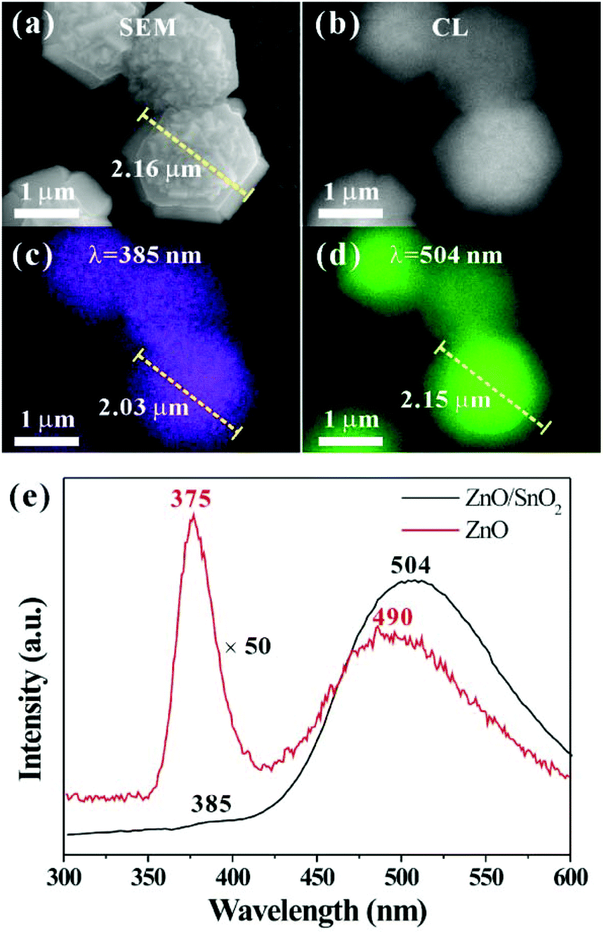 | ||
| Fig. 9 (a) SEM image and (b) full CL image of the ZnO/SnO2-F micropyramids synthesized at a deposition time of 180 s and flow rate of 30 sccm; (c,d) spatial resolved monochromatic CL images recorded at 385 nm and 504 nm emission, respectively; (e) corresponding room-temperature CL spectra of hexagonal micropyramids before and after SnO2 coating. | ||
In order to explore the origin of the enhancement of green emission of the ZnO/SnO2-F core–shell micropyramids, spatial resolved monochromatic CL images of ZnO/SnO2-F micropyramids were measured. As shown in Fig. 9c,d, the size of the green emission domain is roughly consistent with the corresponding SEM image, whereas the UV emission domain is smaller by approximately 100 nm. These results indicate that green emission originates from the whole ZnO/SnO2 composite micropyramids rather than the ZnO core. Generally, UV emission of ZnO corresponds to the near-band-edge peak, which is responsible for free excitations of ZnO,29 and the emissions in the visible-light range of 450–600 nm is associated with the recombination of the holes with electrons occupying the singly ionized O vacancy, and other structural defects or impurities.30–32 In this study, intrinsic structural defects in ZnO micropyramids cannot fully account for the dramatic enhancement of the green emission peak and broadening of the green emission domain after SnO2 coating. On the basis of the structural analysis, the large lattice mismatch between ZnO and SnO2 epitaxial interfaces inevitably introduce large amounts of structural defects near the interfaces and in the bulk of the ZnO core and the SnO2 shell. The high-density structural defects would not only weaken UV emission of ZnO, but also greatly enhance green emission at the domain of whole ZnO/SnO2 composite structures. A similar mechanism has also been proposed to explain the optical properties of biaxial and coaxial ZnO/Ge nanowires.33
4. Conclusions
In this paper, we have successfully prepared ZnO/SnO2 core–shell micropyramids and corresponding SnO2 hollow micropyramids by a simple CVD process and subsequent acid etching treatment. By controlling appropriate deposition times and flow rates of the precursor gas, the SnO2 epitaxial layer can form well-arranged 1D nanostructures or continuous thick films on different surfaces of ZnO micropyramids. Detailed structural analysis demonstrated that the lattice mismatch strain between two epitaxial crystals played a crucial role in determining the different growth status of SnO2 on the ZnO surfaces. Compared to the pristine ZnO micropyramids, the as-prepared pyramidal ZnO/SnO2 core–shell heterostructures exhibited extremely strong green luminescence due to the presence of abundant structural defects in the ZnO and SnO2 heterostructures. Besides their luminescent properties, such ZnO/SnO2 micropyramids are expected to have potential applications in other fields due to the well-known synergistic effect, such as in gas sensing and photocatalysis.Acknowledgements
This work was supported by the National Natural Science Foundation of China (21171142), the National Basic Research Program of China (2011CBA00508), the program for New Century Excellent Talents in University (NCET-11-0294), and the Fundamental Research Funds for the Central Universities.Notes and references
- L. J. Lauhon, M. S. Gudiksen, C. L. Wang and C. M. Lieber, Nature, 2002, 420, 57–61 CrossRef CAS PubMed.
- J. Y. Lao, J. G. Wen and Z. F. Ren, Nano Lett., 2002, 2, 1287–1291 CrossRef CAS.
- D. F. Zhang, L. D. Sun, C. J. Jia, Z. G. Yan, L. P. You and C. H. Yan, J. Am. Chem. Soc., 2005, 127, 13492–13493 CrossRef CAS PubMed.
- K. Nagashima, T. Yanagida, H. Tanaka, S. Seki, A. Saeki, S. Tagawa and T. Kawai, J. Am. Chem. Soc., 2008, 130, 5378–5382 CrossRef CAS PubMed.
- Z. Guo, X. Chen, J. Li, J. H. Liu and X. J. Huang, Langmuir, 2011, 27, 6193–6200 CrossRef CAS PubMed.
- L. Q. Mai, F. Yang, Y. L. Zhao, X. Xu, L. Xu and Y. Z. Luo, Nat. Commun., 2011, 2, 381 CrossRef PubMed.
- J. Q. Hu, Y. Bando and D. Golberg, J. Mater. Chem., 2009, 19, 330–343 RSC.
- A. J. Mieszawska, R. Jalilian, G. U. Sumanasekera and F. P. Zamborini, Small, 2007, 3, 722–756 CrossRef CAS PubMed.
- J. Noborisaka, J. Motohisa, S. Hara and T. Fukui, Appl. Phys. Lett., 2005, 87, 093109 CrossRef PubMed.
- K. Wang, J. J. Chen, Z. M. Zeng, J. Tarr, W. L. Zhou, Y. Zhang, Y. F. Yan, C. S. Jiang, J. Pern and A. Mascarenhas, Appl. Phys. Lett., 2010, 96, 123105 CrossRef PubMed.
- P. Reiss, M. Protiere and L. Li, Small, 2009, 5, 154–168 CrossRef CAS PubMed.
- C. Wang, J. C. Zhao, X. M. Wang, B. X. Mai, G. Y. Sheng, P. Peng and J. M. Fu, Appl. Catal., B, 2002, 39, 269–279 CrossRef CAS.
- W. W. Wang, Y. J. Zhu and L. X. Yang, Adv. Funct. Mater., 2007, 17, 59–64 CrossRef CAS.
- Q. Kuang, Z. Y. Jiang, Z. X. Xie, S. C. Lin, Z. W. Lin, S. Y. Xie, R. B. Huang and L. S. Zheng, J. Am. Chem. Soc., 2005, 127, 11777–11784 CrossRef CAS PubMed.
- H. W. Kim and S. H. Shim, Appl. Surf. Sci., 2006, 253, 510–514 CrossRef CAS PubMed.
- K. Y. Pan, Y. H. Lin, P. S. Lee, J. M. Wu and H. C. Shih, J. Nanomater., 2012, 2012, 279245 Search PubMed.
- J. W. Zhao, C. H. Ye, X. S. Fang, L. R. Qin and L. D. Zhang, Cryst. Growth Des., 2006, 6, 2643–2647 CAS.
- Z. Q. Liu, L. X. Ding, Z. L. Wang, Y. C. Mao, S. L. Xie, Y. M. Zhang, G. R. Li and Y. X. Tong, CrystEngComm, 2012, 14, 2289–2295 RSC.
- C. W. Cheng, B. Liu, H. Y. Yang, W. W. Zhou, L. Sun, R. Chen, S. F. Yu, J. X. Zhang, H. Gong, H. D. Sun and H. J. Fan, ACS Nano, 2009, 3, 3069–3076 CrossRef CAS PubMed.
- X. Zhou, Z. X. Xie, Z. Y. Jiang, Q. Kuang, S. H. Zhang, T. Xu, R. B. Huang and L. S. Zheng, Chem. Commun., 2005, 5572–5574 RSC.
- Q. Kuang, T. Xu, Z. X. Xie, S. C. Lin, R. B. Huang and L. S. Zheng, J. Mater. Chem., 2009, 19, 1019–1023 RSC.
- M. H. Grabow and G. H. Gilmer, Surf. Sci., 1988, 194, 333–346 CrossRef CAS.
- Y. W. Zhang, A. F. Bower and P. Liu, Thin Solid Films, 2003, 424, 9–14 CrossRef CAS.
- S. C. Jain, H. E. Maes, K. Pinardi and I. DeWolf, J. Appl. Phys., 1996, 79, 8145–8165 CrossRef CAS PubMed.
- Y. Ohno, T. Nitta, S. Shimomura and S. Hiyamizu, J. Cryst. Growth, 2001, 227–228, 970–974 CrossRef CAS.
- Y. Chen, D. A. A. Ohlberg and R. S. Williams, J. Appl. Phys., 2002, 91, 3213–3218 CrossRef CAS PubMed.
- R. Ragan, Y. Chen, D. A. A. Ohlberg, G. Medeiros-Ribeiro and R. S. Williams, J. Cryst. Growth, 2003, 251, 657–661 CrossRef CAS.
- Z. M. M. Wang, V. P. Kunets, Y. Z. Z. Xie, M. Schmidbauer, V. G. Dorogan, Y. I. Mazur and G. J. Salamo, Phys. Lett. A, 2010, 375, 170–173 CrossRef CAS PubMed.
- M. H. Huang, S. Mao, H. Feick, H. Q. Yan, Y. Y. Wu, H. Kind, E. Weber, R. Russo and P. D. Yang, Science, 2001, 292, 1897–1899 CrossRef CAS PubMed.
- H. B. Zeng, G. T. Duan, Y. Li, S. K. Yang, X. X. Xu and W. P. Cai, Adv. Funct. Mater., 2010, 20, 561–572 CrossRef CAS.
- N. E. Hsu, W. K. Hung and Y. F. Chen, J. Appl. Phys., 2004, 96, 4671–4673 CrossRef CAS PubMed.
- X. Zhou, Q. Kuang, Z. Y. Jiang, Z. X. Xie, T. Xu, R. B. Huang and L. S. Zheng, J. Phys. Chem. C, 2007, 111, 12091–12093 CAS.
- L. W. Yin, M. S. Li, Y. Bando, D. Golberg, X. L. Yuan and T. Sekiguchi, Adv. Funct. Mater., 2007, 17, 270–276 CrossRef CAS.
| This journal is © the Partner Organisations 2014 |