
 Open Access Article
 This Open Access Article is licensed under a Creative Commons Attribution-Non Commercial 3.0 Unported Licence
Highly reproducible planar Sb2S3-sensitized solar cells based on atomic layer deposition†
Dae-Hwan
Kim‡
a,
Sang-Ju
Lee‡
a,
Mi Sun
Park
a,
Jin-Kyu
Kang
a,
Jin Hyuck
Heo
b,
Sang Hyuk
Im
*b and
Shi-Joon
Sung
 *a
*a
aEnergy Research Division, Daegu Gyeongbuk Institute of Science & Technology, 333, Techno jungang-daero, Hyeonpung-myeon, Dalseong-gun, Daegu 711-873, Republic of Korea. E-mail: imromy@khu.ac.kr; sjsung@dgist.ac.kr; Fax: (+82) 53-785-3739; Tel: (+82) 53-785-3700
bDepartment of Chemical Engineering, Kyung Hee University, 1732, Deogyeong-daero, Giheung-gu, Yongin-si, Gyeonggi-do 446-701, Republic of Korea
First published on 9th October 2014
Abstract
A high-quality Sb2S3 thin-absorber with controllable thickness was reproducibly formed by atomic layer deposition (ALD) technique. Compared with conventional chemical bath deposition (CBD), the Sb2S3 absorber deposited by ALD did not contain oxide or oxygen impurities and showed a very uniform thickness of Sb2S3 absorbers formed on a rough surface of dense blocking TiO2/F-doped SnO2 (bl-TiO2/FTO) substrate. The planar ALD-Sb2S3 solar cells comprised of Au/Poly-3-hexylthiophene/ALD-Sb2S3/bl-TiO2/FTO showed significantly improved power conversion efficiency of 5.77% at 1 sun condition and narrow efficiency deviation, whereas the planar CBD-Sb2S3 solar cells exhibited 2.17% power conversion efficiency. The high efficiency and good reproducibility of ALD-Sb2S3 solar cell devices is attributed to reduced backward recombination because of the inhibition of oxide defects within ALD-Sb2S3 absorber and the conformal deposition of very uniform Sb2S3 absorbers on the blocking TiO2 surface by ALD process.
Introduction
The second generation solar cells such as organic, thin-film, and dye-sensitized solar cells (D-SSCs) have been intensively studied to satisfy the criteria of high efficiency and low cost. Among them, the D-SSCs have been considered as a promising candidate for replacing conventional silicon solar cells owing to a unique device architecture comprised of an electron conductor, sensitizer, and hole conductor. The electrons (holes) generated in the sensitizer by light illumination are immediately transported to the electron (hole) conductor, and consequently less recombination is expected. Therefore, the sensitized solar cells (SSCs) have attracted significant attention since Grätzel et al.1 reported on liquid type D-SSCs and the power conversion efficiency of D-SSCs of up to ∼13% at 100 mW cm−2 AM 1.5 G.2Recently, inorganic semiconductors and quantum dots (QDs) have been of great interest because they can replace the conventional Ru/organic dyes owing to their unique properties, such as strong absorptivity, large dielectric constant, multiple exciton generation, and good stability.3,4 Hence, many metal chalcogenides, including CdS(e),5–8 PbS(e),9–11 and Sb2S(e)3,12–18 have been used as new sensitizers and their device efficiencies have been stiffly increased to over 7% at 1 sun condition.19 Among them, the Sb2S3 exhibited peculiar characteristics. It forms an amorphous phase on the TiO2 electrode at the initial processing stage, and then it is converted to crystalline stibnite by subsequent heat treatment. This may lead to the formation of an intimate junction at the TiO2–Sb2S3 interface, and thus enabling the Sb2S3-SSCs to hold high device efficiencies.
To date, the Sb2S3 has been synthesized by aqueous based chemical bath deposition (CBD) method20 to form a conformal thin-film on the TiO2 electrode. However, the formation of antimony oxides cannot be avoided by the conventional aqueous phase CBD technique and further improvement of device performance appears to be retarded because the antimony oxides make deep traps in the gap state and cause the backward recombination of generated charge carriers.21 Recently, Maiti et al.22 reported the non-aqueous phase CBD technique for the formation of Sb2S3 using a single source precursor, which showed significant depression in the formation of antimony oxides. Very recently, Choi et al.19 demonstrated that the antimony oxides formed by conventional CBD method can be recovered as Sb2S3 by post organic sulfur treatment. It is prerequisite to form pure Sb2S3 through certain deposition processes in order to develop efficient Sb2S3-SSCs.
It is also equally important to develop highly reproducible Sb2S3-SSCs with a narrow deviation of device efficiency. To make reproducible Sb2S3-SSCs, the uniform thickness control of Sb2S3 light absorber is crucial. With this regards, the conventional CBD method has an intrinsic disadvantage because the thickness of Sb2S3 is significantly dependent on heterogeneous nucleation and growth processes, chemical reactions, and consequently its thickness is not linearly dependent on the reaction time. Moreover, the atomic layer deposition (ALD) is a very powerful technique to linearly control the thickness of thin films, and recently Wedemeyer et al.23 demonstrated the possibility of ALD technique to form uniform Sb2S3 layers. Therefore, we adapted the ALD technique in order to precisely control the thickness of the Sb2S3 layer and to form the pure Sb2S3 phase. Through the systematic thickness control of the Sb2S3 layer, we demonstrated that highly reproducible planar Sb2S3-SSCs with 5.77% power conversion efficiency at 1 sun illumination could be obtained.
Experimental
The amorphous Sb2S3 was initially obtained by the ALD of tris-dimethylamino antimony (Sb(N(CH3)2)3; UP Chemical Co., Ltd) and H2S (99.5%, Matheson) gas onto a FTO/bl-TiO2 substrate (15 Ω cm−1, Pilkington) in a showerhead type ALD system (CN1 Co., Ltd, ATOMIC PREMIUM) at 130 °C. The bl-TiO2 layer of ∼70 nm thickness was deposited by spray pyrolysis and annealed at 450 °C. Pulse, exposure, and purge times of (Sb(N(CH3)2)3 are 0.5 s, 10 s, and 10 s; Pulse and purge times of H2S are 3 s and 10 s.To convert the amorphous phase to crystalline one, the atomic layer deposited yellowish films of amorphous Sb2S3/bl-TiO2/FTO were annealed at 330 °C for 30 min under H2S gas. After annealing, dark-brown crystalline stibnite Sb2S3/bl-TiO2/FTO was immediately removed from the heater and cool down under N2. As an organic hole transporting material (HTM), poly-3-hexylthiophene (P3HT; Rieke metals, Inc.) was used. The solution of the HTM (15 mg mL−1 in 1,2-dichlorobenzene) was spin-coated onto the dense TiO2/Sb2S3 layer with 2500 rpm for 60 s. Then, in order to improve the contact between P3HT and Au, a poly(3-4-ethylenedioxythiophene) doped with poly(4-styrenesulfonate) (PEDOT:PSS; Baytron AI4083) diluted with six volumes of 2-propanol was spin-coated onto the P3HT/Sb2S3/bl-TiO2 at 2000 rpm for 30 s. In order to form a hybrid heterojunction, the dense TiO2/Sb2S3/P3HT/PEDOT:PSS layer was annealed at 90 °C for 30 min in vacuum oven. Finally, the counter electrode was deposited by thermal evaporation of gold under a pressure of 5 × 10⁻⁶ Torr giving an active area of 0.16 cm2 for each device.
J–V data were measured using a solar simulator (Newport, 94022A) at 1 sun condition (AM 1.5 G, 100 mW cm–2) and under varied intensity of illumination by a source meter (Keithley 2400) equipped with a calibrated Si-reference cell (certified by NREL). The external quantum efficiencies (EQE) of solar cells were analyzed using an Incident Photon-to-Current Efficiency (IPCE) measurement system (McScience co., LTD, K3100) consisting of a 300 W xenon lamp, a monochromator (Spectral Products, CM110), and a multimeter (Keithley 2400). In order to eliminate experimental errors, four different cells with the same structure were fabricated using the same procedure, and all the measurements were carried out five times and averaged. Photovoltaic performance was measured by using a metal mask with an aperture area of 0.096 cm2.
Ellipso Technology Elli-SE-aM8 variable angle spectroscopic ellipsometer was used to obtain the thickness of the Sb2S3 thin film and confirmed by FE-SEM (Hitachi SU8020). The UV-visible diffuse absorbance spectra of the Sb2S3 films were obtained using a Perkin Elmer Lambda 750 UV/VIS spectrometer with an integrating sphere. XPS spectra were obtained with an ESCALAB 250Xi (Thermo Scientific, UK) system using a microfocused (500 μm, 157 W) Al Kα X-ray beam with a photoelectron takeoff angle of 90°. A dual-beam charge neutralizer (1 eV Ar+ and 1 eV electron beams) was used to compensate for the charge-up effect. Ar+ ion source was operated at 3 μA and 2 kV, with rastering on an area of 4 mm × 2 mm. The XPS spectra of the CBD-Sb2S3 and ALD-Sb2S3 were obtained after Ar sputtering for 60 s. The cross-sectional morphology of the device was measured by FE-TEM (Hitachi, HF3300) with FIB systems (NB5000).
Results and discussion
Fig. 1 shows a schematic illustration of the formation of Sb2S3 layer on the blocking TiO2 (bl-TiO2)/FTO (F doped SnO2) substrate by conventional CBD and ALD processes. In the CBD process, as illustrated in Fig. 1a, the thickness of the Sb2S3 layer is determined by the rate of chemical reaction, and thus the precise temperature control of the reaction bath is very important. In addition, it is very difficult to reproducibly make uniform thickness of the Sb2S3 layer, even in the same reaction process, because the heterogeneous nucleation condition of Sb2S3 on bl-TiO2/FTO substrate will depend on the surface state of bl-TiO2/FTO substrate. Therefore, the CBD method causes a larger thickness deviation of the Sb2S3 layer and makes it difficult for the Sb2S3-SSCs to show reproducible device performance with narrow efficiency deviation. It should also be considered that the formation of antimony oxides is inevitable when we deposit the Sb2S3 layer through aqueous phase chemical reaction.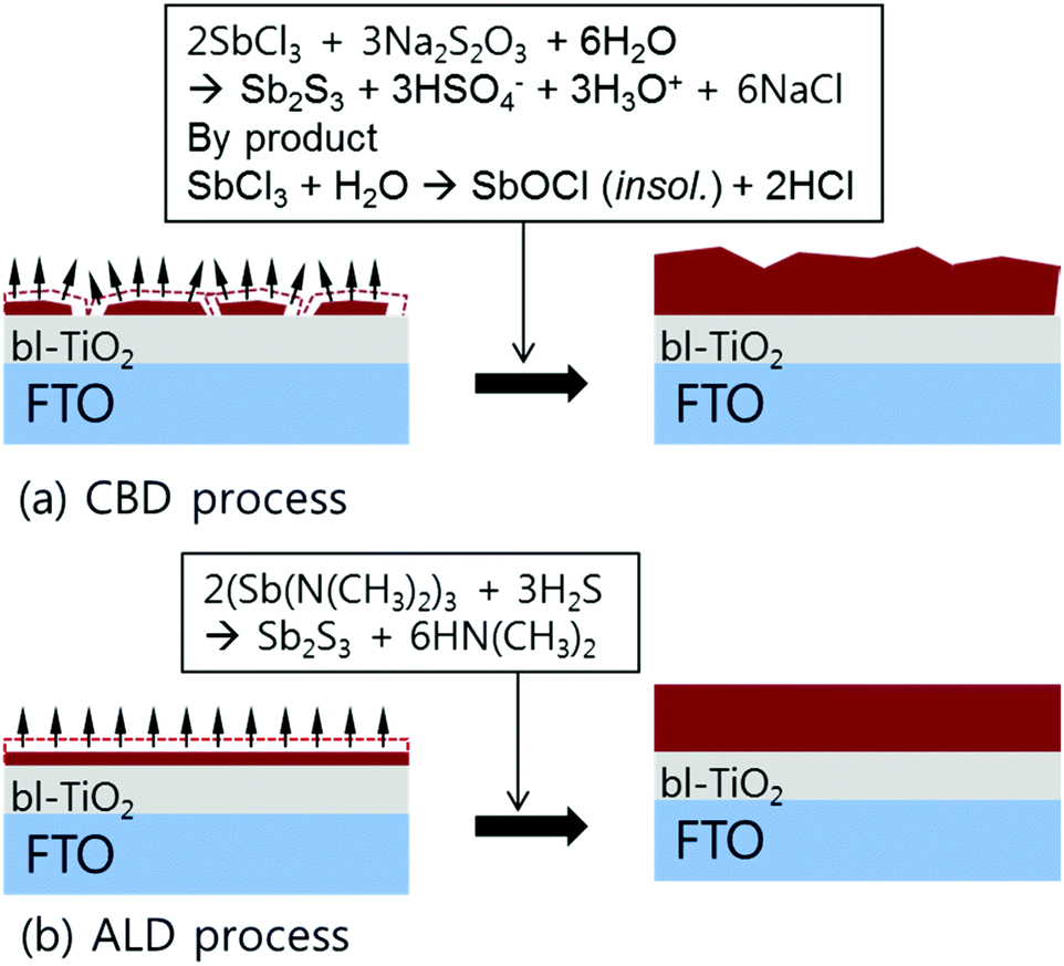 | ||
| Fig. 1 Schematic illustration for the formation of Sb2S3 thin-layer on the bl-TiO2/FTO substrate by CBD and ALD process. | ||
On the other hand, the ALD process does not include any oxygen sources for any of the chemical reactions, and consequently it is expected that the formation of antimony oxides will be significantly suppressed. The thickness of Sb2S3 layer on bl-TiO2/FTO substrate can also be precisely controlled as shown in Fig. 1b because the formation of Sb2S3 is physically controlled by the repeated chemical reaction of the specific amount of precursors.
Fig. 2a and b show the typical cross-sectional TEM images of the Sb2S3/bl-TiO2/FTO substrates. Compared with the CBD-Sb2S3, the ALD-Sb2S3 thin layer with about 90 nm thickness was more uniformly deposited along the rough FTO/dense-TiO2 surfaces. The magnified image of each inset shows that the ALD-Sb2S3 film is more densely formed than the CBD-Sb2S3 film because the later exhibited some pores within the film structure, which may have been formed by the thermal annealing process to convert its amorphous phase to crystalline one because the particle-like amorphous Sb2S3 are aggregated to form the film structure, which is converted to polycrystalline film through volume shrinkage by phase change. One of the merits of ALD process is the precise control of the thin film deposition by controlling ALD cycles. In order to investigate the deposition rate of Sb2S3 thin films by ALD process, we measured the thickness of Sb2S3 thin films with the number of ALD cycles as shown in Fig. 2c. From the thickness data quantified by spectroscopic ellipsometry, it was found that the thickness of Sb2S3 thin films linearly depends on the number of ALD cycles up to 4000 and the deposition rate of Sb2S3 was about 0.56 Å per cycle. As expected, this confirms that the ALD process can reproducibly deposit the Sb2S3 thin films, which will enable the Sb2S3-SSCs to have reproducible device efficiency. Moreover, the thickness of CBD-Sb2S3 films exhibited exponential increase with the deposition time and larger thickness-deviation compared to ALD-Sb2S3, which indicated that the device will also have larger efficiency deviation.
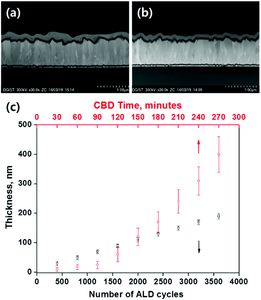 | ||
| Fig. 2 A representative cross-sectional TEM image of (a) CBD-Sb2S3 (90 nm ± 30 nm) and (b) ALD-Sb2S3 (90 nm ± 6 nm) formed on bl-TiO2 (∼70 nm)/FTO (450 nm); and (c) the thickness of Sb2S3 layer deposited on a bare glass plate by ALD and CBD process. | ||
The purity of Sb2S3 sensitizer is very important because the conventional CBD-Sb2S3 formed in aqueous phase synthesis yields the formation of antimony oxide, and subsequently deep traps below 1.03 eV19 from its conduction band energy are formed. The deep traps lead the injected electrons from the Sb2S3 sensitizer to the TiO2 electron conductor to be transferred backward in direction and cause the recombination of electrons and holes, while deteriorating the open circuit voltage (Voc). Therefore, we checked the purity of CBD-Sb2S3 and ALD-Sb2S3 using X-ray photo electron spectroscopy (XPS) spectra as shown in Fig. 3. Fig. 3a shows that the deconvolution of the Sb 3d core level exhibits two chemical states of Sb2S3 (1 and 1′), Sb2O3 (2 and 2′) and an overlapping oxygen peak (3). These spectra clearly confirm that the Sb2S3 thin films deposited by conventional aqueous CBD process contains some amount of oxide. However, XPS spectra of Sb2S3 deposited by ALD process showed single peaks, corresponding to a single chemical state of Sb2S3 (1 and 1′), and there was no oxide or oxygen peak, as shown in Fig. 3b.22,24 From these XPS analyses, it was found that high quality Sb2S3 thin films without any oxide or oxygen impurities could be successfully deposited by ALD process, which might be advantageous for achieving high performance Sb2S3 solar cells.
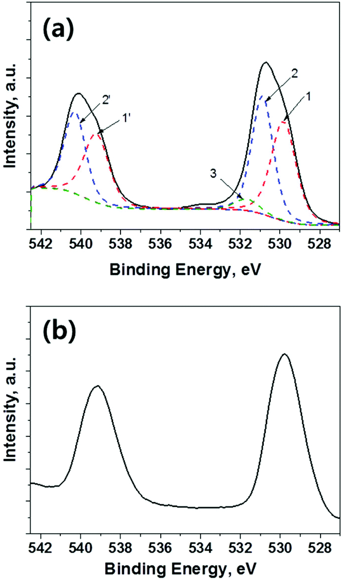 | ||
| Fig. 3 XPS Sb 3d spectra of Sb2S3 obtained from the (a) conventional CBD process and (b) ALD process. The solid line is experimental data and dot line is fitted data. 1 (Sb2S3) = Sb 3d5/2, 1′ (Sb2S3) = Sb 3d3/2, 2 (Sb2O3) = Sb 3d5/2, 2′ (Sb2O3) = Sb 3d3/2, 3 = O 1 s. | ||
Fig. 4a shows the diffuse reflection spectra of ALD-Sb2S3 with the number of repeated ALD cycles, where the thickness of ALD 400, 1000, 1600, and 2200 cycles correspond to 30 nm ± 6 nm, 60 nm ± 7 nm, 90 nm ± 6 nm, and 120 nm ± 7 nm. The absorption tail is gradually red-shifted with the thickness of ALD-Sb2S3 layer and is almost saturated over ALD 1600 cycles. Fig. 4b and Table 1 show the current density–voltage (J–V) curves and the photovoltaic parameters (short circuit current density, open circuit voltage, fill factor, and power conversion efficiency: Jsc, Voc, FF, and η) of CBD- and ALD-Sb2S3 devices. A conventional FTO/bl-TiO2/CBD-Sb2S3/P3HT/Au device showed Voc of 0.4886 V, Jsc of 9.63 mA cm−2, FF of 46.13%, and η of 2.17%, which are similar in result with previously reported planar Sb2S3-SSCs (Voc = 0.56 V, Jsc = 7.15 mA cm−2, FF = 35%, η = 1.43%).25 Here, it is noted that the CBD 120 min sample exhibited the best device efficiency when we checked the efficiency of planar Sb2S3-SSCs with the CBD time (the thickness of CBD-Sb2S3 120 min sample is shown in Fig. 2a).
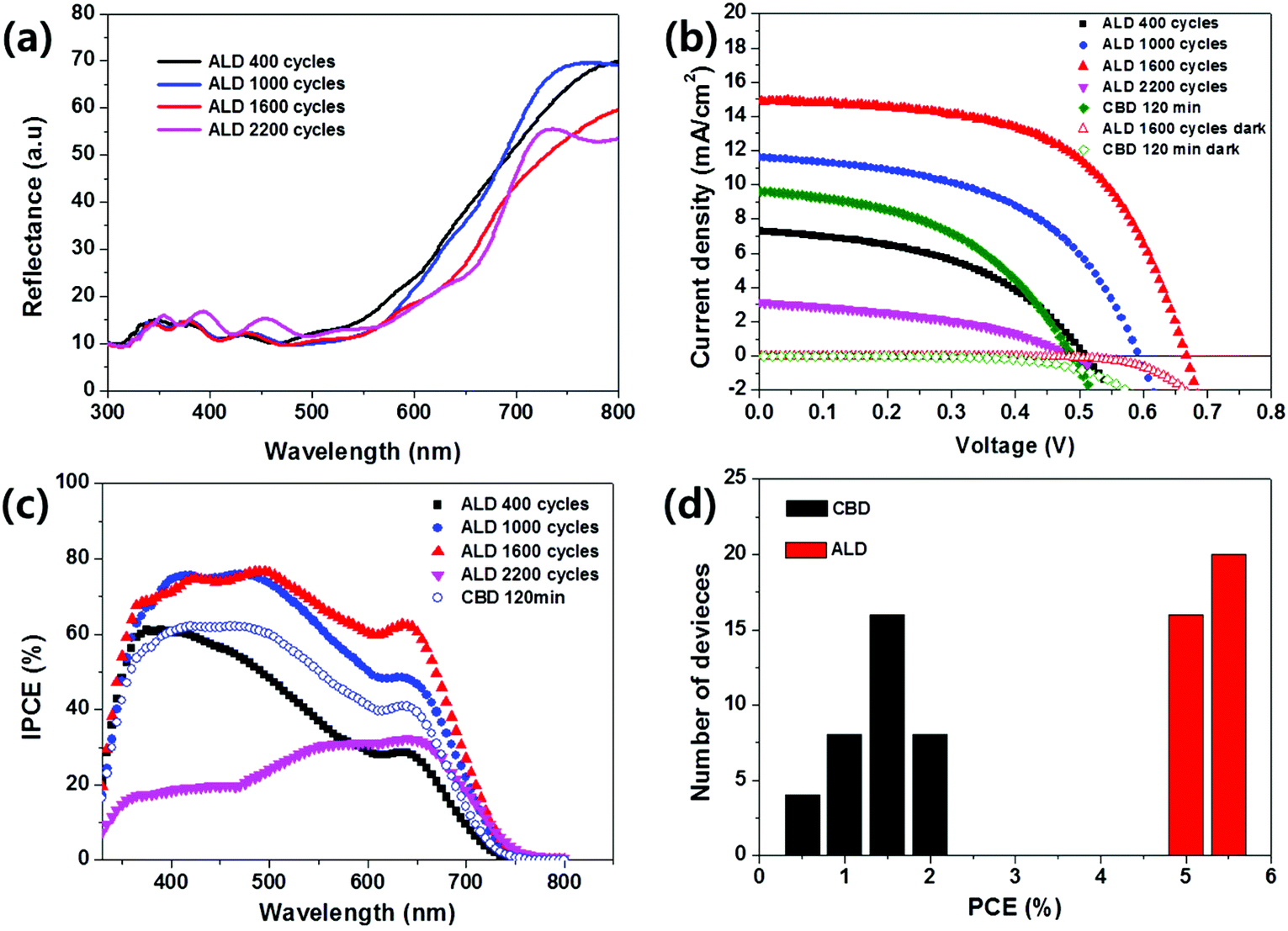 | ||
| Fig. 4 (a) Diffuse reflection spectra of ALD-Sb2S3 deposited on bl-TiO2/FTO substrates for various ALD cycles, (b) current density–voltage (J–V) curves, and (c) IPCE spectra of planar FTO/bl-TiO2/Sb2S3/P3HT/PEDOT:PSS/Au fabricated by different ALD cycles and CBD 120 min; and (d) PCE distribution of 36 planar Sb2S3-SSC samples fabricated by ALD 1600 cycles and CBD 120 min. | ||
| Sb2S3 (cycles) | V oc (V) | J sc (mA cm−2) | FF (%) | η (%) |
|---|---|---|---|---|
| ALD 400 | 0.5105 | 7.28 | 46.17 | 1.72 |
| ALD 1000 | 0.5937 | 11.60 | 51.15 | 3.52 |
| ALD 1600 | 0.6665 | 14.92 | 58.04 | 5.77 |
| ALD 2200 | 0.4872 | 3.13 | 40.54 | 0.62 |
| CBD 120 min | 0.4886 | 9.63 | 46.13 | 2.17 |
On the other hand, FTO/bl-TiO2/ALD-Sb2S3/P3HT/Au devices exhibited dramatically enhanced photovoltaic performance, depending on the ALD cycles of Sb2S3; the Jsc enhanced with increased ALD cycle of Sb2S3 up to 1600 cycles, and then decreased with further increase in the ALD cycle. We also confirmed the enhancement of Voc with an increase of the ALD cycle of Sb2S3 up to 1600 cycles, and then a decrease of Voc with the 2200 ALD cycle. All of ALD-Sb2S3 solar cells showed higher Voc value compared with CBD-Sb2S3, which might be attributed to the formation of more pure Sb2S3 absorbers without impurities as confirmed by XPS analysis in Fig. 3. The best device under air mass 1.5 global (AM 1.5 G) and full sunlight (100 mW cm−2) exhibited Jsc, Voc, and FF values of 14.92 mA cm−2, 0.667 V, and 58.04%, respectively, yielding η of 5.77%, which is three-fold higher than that of the CBD Sb2S3 device.
In order to investigate the light response of Sb2S3 devices, we measured IPCE (Incident photon-to-current conversion efficiency) of CBD-Sb2S3 and ALD-Sb2S3 thin film solar cells (Fig. 4c). Compared with CBD-Sb2S3, ALD-Sb2S3 solar cells with 1000 and 1600 ALD cycle showed higher IPCE, although the absorption spectra edges of CBD-Sb2S3 and ALD-Sb2S3 were the same near 750 nm wavelength because the average thickness of Sb2S3 (CBD 120 min and ALD 1000 cycles) was the same to ∼90 nm (see Fig. 2a and b).
It should be noted that despite planar type solar cells, the planar ALD-Sb2S3-SSCs exhibited excellent photovoltaic performance compared with the planar CBD-Sb2S3 device and the mesoscopic CBD-Sb2S3-SSCs with P3HT hole conductor.26 The improved performance of ALD-Sb2S3 solar cells might be attributed to the high purity Sb2S3 absorbers compared with conventional CBD-Sb2S3 absorbers because (1) the dark current leakage of ALD-Sb2S3 sample could be blocked even at higher bias voltage than that of the CBD-Sb2S3 sample as shown in Fig. 4b, which consequently enables the ALD-Sb2S3 to have higher Voc;27 and (2) the charge transfer and/or the charge collection efficiency of the ALD-Sb2S3 sample could be significantly improved from those of the CBD-Sb2S3 sample, owing to the similar light harvesting efficiency at same thickness of Sb2S3 absorber, since IPCE is the product of light harvesting efficiency, charge transfer efficiency, and charge collection efficiency.
From thickness analysis of ALD-Sb2S3 thin films (Fig. 2), it was found that the controllability and uniformity of ALD-Sb2S3 films were considerably better than those of the conventional CBD-Sb2S3. This reproducible formation of Sb2S3 with small thickness-deviations by ALD process will guarantee the reproducibility of solar cell devices with small efficiency-deviations, which is a crucial factor for commercialization of solar cells. To confirm the reproducibility of solar cell devices, the PCE (η) histogram of each individually fabricated solar cell device using CBD-Sb2S3 and ALD-Sb2S3 was exhibited, as shown in Fig. 4d. The PCE histogram indicates that ALD-Sb2S3 solar cells show not only higher PCE, but also narrow distribution of PCE compared with CBD-Sb2S3 solar cells. This result shows that the ALD process for the formation of Sb2S3 absorbers is a promising fabrication tool for reproducible solar cells.
Fig. 5a and b show the UPS spectra of Sb2S3 films deposited on bl-TiO2 by CBD and ALD processes. The work function is determined from the photon energy and the high binding energy cutoff of the UPS spectrum, corrected for a −5 V bias. The high binding energy cutoff is 16.56 and 16.46 V for ALD-Sb2S3 and CBD-Sb2S3, respectively (Fig. 5a), and low binding energy onset of ALD-Sb2S3 and CBD-Sb2S3 is 1.26 and 1.10 V, respectively (Fig. 5b). The work function was calculated by the equation, Φ = 21.22 – high binding energy cutoff, giving the position of the Fermi level as 4.66 and 4.76 eV for ALD-Sb2S3 and CBD-Sb2S3, respectively. By adding the low binding energy onset to the UPS spectrum, the valence band maximum with respect to the vacuum level can be calculated. The conduction band minimum is determined by adding an optical band gap of Sb2S3, 1.76 eV, which is estimated from the IPCE spectra (Fig. 4c). From these results, it was possible to illustrate the energy band diagrams of the ALD-Sb2S3 and CBD-Sb2S3 devices (Fig. 5c). The ALD-Sb2S3 showed 0.1 eV higher Fermi levels compared with the CBD-Sb2S3, which might be attributed to the formation of purer Sb2S3 sensitizers by the ALD process, because the oxide impurities make defect states in Sb2S3 absorbers and consequently the Voc is deteriorated. Therefore, the higher Voc of ALD-Sb2S3-SSCs compared with that of CBD-Sb2S3-SSCs, as shown in Fig. 4 and Table 1, could be explained by the higher Fermi-level of ALD-Sb2S3 absorbers.
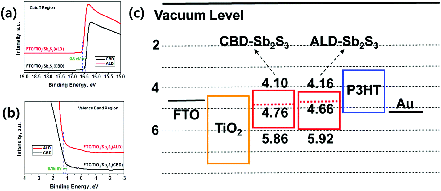 | ||
| Fig. 5 UPS spectra at (a) cutoff region, and (b) valence band region for FTO/bl-TiO2/ALD-Sb2S3 and FTO/bl-TiO2/CBD-Sb2S3 samples; and (c) corresponding energy band diagram of planar ALD-Sb2S3- and CBD-Sb2S3-SSC. | ||
Conclusions
We could fabricate reproducible planar Sb2S3-SSCs with 5.77% power conversion efficiency with narrow efficiency-deviation by ALD technique, whereas the planar Sb2S3-SSCs fabricated by the conventional CBD method exhibited poor power conversion efficiency with wide deviation. The high reproducibility of ALD-Sb2S3-SSCs was attributed to the conformal deposition of very uniform Sb2S3 thin-layers with narrow deviation on bl-TiO2/FTO substrate. Moreover, the CBD method yielded the formation of rough Sb2S3 thin-layers with wide deviation because the deposition rate of Sb2S3 thin-layers was nonlinear to reaction time and very sensitive to reaction temperature. The high device efficiency was attributed to the formation of pure Sb2S3 free of oxide because no oxygen source is involved during the entire ALD process, whereas the aqueous phase based CBD inevitably forms antimony oxide. Therefore, the ALD-Sb2S3-SSCs exhibited high open circuit voltage, short circuit current density, and high fill factor due to the reduced backward recombination by large suppression of oxide defects within the Sb2S3-sensitizers.Acknowledgements
This work was supported by DGIST R&D Program of the Ministry of Education, Science and Technology of Korea (14-EN-03).Notes and references
- B. O'regan and M. Grätzel, Nature, 1991, 353, 737 CrossRef.
- S. Mathew, A. Yella, P. Gao, R. Humphry-Baker, B. F. Curchod, N. Ashari-Astani, I. Tavernelli, U. Rothlisberger, M. K. Nazeeruddin and M. Grätzel, Nat. Chem., 2014, 6, 242 CrossRef CAS PubMed.
- A. J. Nozik, Chem. Phys. Lett., 2008, 457, 3 CrossRef CAS PubMed.
- R. Costi, A. E. Saunders and U. Banin, Angew. Chem., Int. Ed., 2010, 49, 4878 CrossRef CAS PubMed.
- Y. L. Lee and Y. S. Lo, Adv. Funct. Mater., 2009, 19, 604 CrossRef.
- J. H. Bang and P. V. Kamat, Adv. Funct. Mater., 2010, 20, 1970 CrossRef CAS.
- S. H. Im, Y. H. Lee and S. I. Seok, Electrochim. Acta, 2010, 55, 5665 CrossRef CAS PubMed.
- S. H. Im, Y. H. Lee, S. I. Seok, S. W. Kim and S.-W. Kim, Langmuir, 2010, 26, 18576 CrossRef CAS PubMed.
- S. H. Im, H.-j. Kim, S. W. Kim, S.-W. Kim and S. I. Seok, Energy Environ. Sci., 2011, 4, 4181 CAS.
- J. Jean, S. Chang, P. R. Brown, J. J. Cheng, P. H. Rekemeyer, M. G. Bawendi, S. Gradečak and V. Bulović, Adv. Mater., 2013, 25, 2790 CrossRef CAS PubMed.
- J. Y. Kim, O. Voznyy, D. Zhitomirsky and E. H. Sargent, Adv. Mater., 2013, 25, 4986 CrossRef CAS PubMed.
- Y. Itzhaik, O. Niitsoo, M. Page and G. Hodes, J. Phys. Chem. C, 2009, 113, 4254 CAS.
- S.-J. Moon, Y. Itzhaik, J.-H. Yum, S. M. Zakeeruddin, G. Hodes and M. Grätzel, J. Phys. Chem. Lett., 2010, 1, 1524 CrossRef CAS.
- S. H. Im, H.-j. Kim, J. H. Rhee, C.-S. Lim and S. I. Seok, Energy Environ. Sci., 2011, 4, 2799 CAS.
- S. H. Im, C.-S. Lim, J. A. Chang, Y. H. Lee, N. Maiti, H.-J. Kim, M. K. Nazeeruddin, M. Grätzel and S. I. Seok, Nano Lett., 2011, 11, 4789 CrossRef CAS PubMed.
- Y. C. Choi, Y. H. Lee, S. H. Im, J. H. Noh, T. N. Mandal, W. S. Yang and S. I. Seok, Adv. Energy Mater., 2014, 4, 1301680 Search PubMed.
- K. Tsujimoto, D.-C. Nguyen, S. Ito, H. Nishino, H. Matsuyoshi, A. Konno, G. R. A. Kumara and K. Tennakone, J. Phys. Chem. C, 2012, 116(25), 13465 CAS.
- S. Ito, K. Tsujimoto, D.-C. Nguyen, K. Manabe and H. Nishino, Int. J. Hydrogen Energy, 2013, 38, 16749 CrossRef CAS PubMed.
- Y. C. Choi, D. U. Lee, J. H. Noh, E. K. Kim and S. I. Seok, Adv. Funct. Mater., 2014, 24, 3587 CrossRef CAS.
- S. Messina, M. Nair and P. Nair, Thin Solid Films, 2007, 515, 5777 CrossRef CAS PubMed.
- D. U. Lee, S. W. Pak, S. G. Cho, E. K. Kim and S. I. Seok, Appl. Phys. Lett., 2013, 103, 023901 CrossRef PubMed.
- N. Maiti, S. H. Im, C.-S. Lim and S. I. Seok, Dalton Trans., 2012, 41, 11569 RSC.
- H. Wedemeyer, J. Michels, R. Chmielowski, S. Bourdais, T. Muto, M. Sugiura, G. Dennler and J. Bachmann, Energy Environ. Sci., 2013, 6, 67 CAS.
- C. P. Liu, H. E. Wang, T. W. Ng, Z. H. Chen, W. F. Zhang, C. Yan, Y. B. Tang, I. Bello, L. Martinu, W. J. Zhang and S. K. Jha, Phys. Status Solidi B, 2011, 249, 627 CrossRef.
- P. P. Boix, Y. H. Lee, F. Fabregat-Santiago, S. H. Im, I. Mora-Sero, J. Bisquert and S. I. Seok, ACS Nano, 2011, 6, 873 CrossRef PubMed.
- J. A. Chang, S. H. Im, Y. H. Lee, H.-j. Kim, C.-S. Lim, J. H. Heo and S. I. Seok, Nano Lett., 2012, 12, 1863 CrossRef CAS PubMed.
- J. Y. Hwang, S. A. Lee, Y. H. Lee and S. I. Seok, ACS Appl. Mater. Interfaces, 2010, 2, 1343 CAS.
Footnotes |
| † Electronic supplementary information (ESI) available. See DOI: 10.1039/c4nr04148h |
| ‡ These two authors have equally contributed to this work. |
| This journal is © The Royal Society of Chemistry 2014 |