 Open Access Article
 This Open Access Article is licensed under a
 Creative Commons Attribution 3.0 Unported Licence
The hybrid concept for realization of an ultra-thin plasmonic metamaterial antireflection coating and plasmonic rainbow
M. Keshavarz
Hedayati
a,
S.
Fahr
b,
C.
Etrich
b,
F.
Faupel
c,
C.
Rockstuhl
b and
M.
Elbahri
*ad
aNanochemistry and Nanoengineering, Institute for Materials Science, Faculty of Engineering, Christian-Albrechts-Universität zu Kiel, Kaiserstrasse 2, 24143 Kiel, Germany
bInstitute of Condensed Matter Theory and Optics, Abbe Center of Photonics, Friedrich-Schiller-Universität, Jena, Max-Wien-Platz 1, 07743 Jena, Germany
cChair for Multicomponent Materials, Institute for Materials Science, Faculty of Engineering, Christian-Albrechts-Universität zu Kiel, Kaiserstrasse 2, 24143 Kiel, Germany
dInstitute of Polymer Research, Helmholtz-Zentrum Geesthacht, Max-Planck-Str. 1, 21502 Geesthacht, Germany. E-mail: me@tf.uni-kiel.de
First published on 20th March 2014
Abstract
We report on the design, simulation, fabrication, and characterization of a novel two layer anti-reflective coating (ARC) based on a plasmonic metamaterial and a dielectric. Promoted by the strong material dispersion of the plasmonic metamaterial, our novel concept (called hybrid ARC) combines two possible arrangements for layers in an anti-reflection coating into a single structure; albeit at two different wavelengths. This, however, causes a broadband reduction of reflection that is less sensitive against oblique incidence when compared to traditional antireflective coatings. Furthermore, we show that the current metamaterial on a metal reflector can be used for the visualization of different coloration such as plasmonic rainbow despite its sub-wavelength thickness.
The finite reflectivity from the interface of two disparate media with dispersive material properties is an obstacle that often denies the design of efficient photonic and opto-electronic devices.1 Traditionally, the problem can be diminished while incorporating anti-reflection coatings (ARCs)2 that are based on graded index layers,3–6 gradient-index coatings,7,8 or nanostructured textures.9,10 However, these approaches usually suffer from one or multiple severe drawbacks such as a narrow spectral domain of operation, sensitivity against oblique incidence, complexity, or a lack of applicability to extremely thin films. Here, we mitigate these problems by introducing and verifying a new class of ultrathin two-layer anti-reflection coating with a metamaterial as the top and a dielectric material as the second layer; demonstrating therewith an entire novel concept named as “hybrid ARC”. The key feature of this hybrid ARC is using (quasi) two arrangements for the dielectric layers in one design where the refractive indices ascend or descend in consecutive layers with a descending order, albeit at a different wavelength. This is only possible by exploiting the strongly dispersive character of metamaterials. High ARC performance on silicon substrate is shown to be possible by plasmonic nanocomposites with a strong dispersion in the permittivity around its plasmonic resonance. Below the plasmon resonance wavelength the layer acts as a traditional graded-index coating while it performs as a Fabry–Perot interferometer at longer wavelengths. This provides the opportunity to considerably lower the reflection across a broad range of wavelengths with only a marginal angular sensitivity. Moreover, the hybrid concept can be applied on metals where the tunability of the plasmonic nanocomposite enables realization of plasmonic rainbow colors by a sub-wavelength coating.
The consideration of anti-reflective coatings (ARCs) as being very important is justified from their integration in nearly all photonic devices.11–15 Optical elements where they find use range from ordinary lenses over any laser system up to advanced photonic devices for disruptive technologies. Traditional ARCs made from an individual non-absorbing layer can usually be optimized to operate perfectly at an isolated design wavelength. Then, the refractive index (RI) of the ARC (being directly linked to the square root of the permittivity for non-magnetic, homogenous, isotropic, local materials as considered here) has to be the geometric mean of the RIs of the materials on both sides of the respective interface from which the spurious reflection is encountered, i.e. herein called a substrate and the incident medium. By no means of restriction, we consider in the following the RI of the substrate to be larger than the RI of the incident material (coating). The thickness of the ARC ought to be a quarter of the desired wavelength. However, and quite detrimental, the vanishing reflectivity only occurs at normal incidence and only at the isolated design wavelength. Nevertheless, wider-band ARCs are possible by relying on innovative designs,16,17 plasmonic and metamaterial layers18,19 or multilayer coatings.20 For instance, two-layer ARCs,21i.e. ‘V’ coat, could result in a wide-band ARC by a proper selection of films. In such a case the RI of the top layer should be smaller than the second layer and each layer thickness shall equal a quarter of the desired wavelength. The first suggestion for such a traditional arrangement of the layer materials is linked to the name of Lord Rayleigh; hence hereafter we call it the Rayleigh configuration. In fact, the order of the ARC film is very crucial in such a technique and once the order of layers is inversed (i.e. low and high RI placing as the spacer and the top layer, respectively), the reflection of the device increases and could even turn the substrate (in certain circumstances) into a mirror (Bragg-mirror).22,23 We wish to call such an arrangement in the following the reverse-Rayleigh configuration. Note that the in the reverse-Rayleigh configuration at least two reflection dips surround the central reflection peak.24
Recently, a new class of ARCs has been introduced, specifically for metallic substrates where the coating acts as an absorbing element to reduce the light reflection. In such a configuration, the reflection drops not only due to the interference25 but also by exploiting the absorbing character of the coating combined with losses in the metallic substrate.26–34 The strong optical attenuation through the highly absorbing coating or the strong resonant behavior in layers29 gives rise to low reflection from the metal substrate, although the thickness of the coating is much less than the wavelength of light. This concept works well on gold films which could sustain a plasmonic response under certain conditions as well as a broad intrinsic absorption (i.e. minimum reflection) in the visible range because of interband transition. The question arises whether this concept is equally applicable to semi-conductors as the substrate material. It is known that semi-conductors like silicon exhibit strongly dispersive material properties that complicate the design of efficient ARCs. Therefore, it remains a challenge to perceive an ARC that operates over the entire range of the visible and near-IR for semi-conductors.35
Here, we introduce an ultra-thin bi-layer coating as an ARC. The key-feature of our coatings is the use of a material with a high RI for the layer that faces the incident medium, i.e. the top layer. Moreover, the thicknesses of all involved layers are considerably thinner than a half or even a quarter of a wavelength. By a systematic analysis we show that an excellent anti-reflection performance is possible. While demonstrating the concept in the first stage with a pair of dielectric materials possessing only a weak dispersion, i.e. TiO2/SiO2, we exploit the strong dispersive nature of metamaterials in the second stage to demonstrate the hybrid-concept and eventually achieve a broad-band ARC with only a marginal angular sensitivity.
The metamaterial we will use consists of an ultrathin plasmonic nanocomposite made from ultra-fine metallic nanoparticles (diameter D < 5 nm (ref. 26)). Fig. 1a and b show the cross-sectional and top view TEM images of the sample. It is apparent that the particles' diameters are around 5 nanometers and they are randomly distributed in the matrix. It possesses a dispersive permittivity with a Lorentzian profile centered at the particle plasmon resonance. The homogenous isotropic metamaterial is characterized by a strongly dispersive RI that takes high values at long wavelengths and small values at short wavelengths, taken with respect to the particle plasmon resonance. Such a material can therefore beneficially be used to perceive an ARC that combines the reverse-Rayleigh and the Rayleigh ARC in the same structure, albeit at different wavelengths. Therefore, we call this structure a “Hybrid-Antireflection” structure. We postulate that the broadband anti-reflection performance of the presented metamaterial is facilitated by the anomalous material dispersion around the plasmon resonance. The dispersive refractive index of the composite varies in a way that at wavelengths longer than the resonance the coating serves in a reverse-Rayleigh configuration but at smaller wavelengths the composite's RI is smaller than the second layer and hence the Rayleigh condition is satisfied. In other words, by overlapping the reflection dip of the traditional ARC with that of a Fabry–Perot interferometer, the corresponding reflection dip of our two layer coating is very broad despite its low thickness. This unique dispersive RI of the presented metamaterial leads to the opportunity to observe a hybrid wide-band ARC encompassing the Rayleigh/reverse-Rayleigh configurations. Full wave electro-magnetic simulations of the metamaterial verify that it acts as a homogenous medium rather than an ensemble of plasmonic absorbers. This entails their description in terms of effective material properties which paves the way to consider such a structure in the design of many high efficient ARC devices.
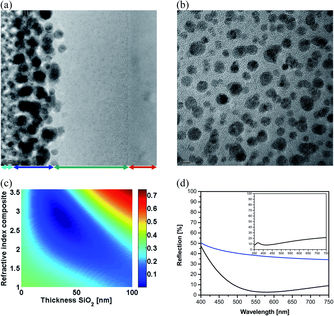 | ||
| Fig. 1 (a) Cross-sectional image of plasmonic nanocomposite in which the arrows indicate each of the samples. Light blue, blue, green and red arrows represent the platinum (top adhesion layer for cutting of the sample), nanocomposite, SiO2 layer and silicon wafer, respectively. (b) Top view TEM image of the plasmonic nanocomposite wherein the dark spheres are the silver particles. (c) Reflection of a 20 nm film with varying RI on a SiO2 film with varying thickness on top of a silicon substrate at a wavelength of 600 nm. (d) (black) Reflection spectrum of a typical reverse-Rayleigh configuration (20 nm TiO2 atop of 50 nm SiO2 coated Silicon) in comparison with bare silicon (blue). The inset shows the reflection spectrum of 50 nm SiO2 atop of 20 nm TiO2 coated silicon (Rayleigh configuration). | ||
To start with, we consider a bi-layer ARC where the top layer facing air as the incident medium is an ultrathin film of a high RI material. With the final device in mind, the thickness is chosen to be 20 nm. This adheres to the desire to have an ultra-thin and compact ARC. We leave here the exact value of the RI as a free parameter. The second layer shall be made from a low RI material. Silicon dioxide is selected as the low RI film since it is a common material in silicon industry and it can be either deposited or grown on the silicon substrate with good adhesion. We leave as a degree of freedom the thickness of this layer. In such a scheme, the substrate, i.e. silicon wafer, has the highest RI in the stack.
To identify on analytical grounds the conditions where the ARC operates optimal, a thin-film transfer matrix technique is applied to calculate the reflection. Results are shown in Fig. 1c. There, the reflectivity at a design wavelength (in this case at 600 nm) is calculated depending on the RI of the top layer and the thickness of the SiO2 layer. It is apparent that the reflection is suppressed for a rather high value of RI of the ultrathin top layer and a thin SiO2 layer. To suppress reflectivity at longer design wavelengths, the RI should be approximately the same but the thickness of the SiO2 layer should be slightly increased. However, it can always be assured that the reflection can be reduced to a negligible quantity, even though the coating is sub-wavelength in its thickness, i.e. far below the quarter of the design wavelength.
According to the calculated reflection contour (Fig. 1c), a high RI material which suitably matches the required RI is TiO2 (its average RI in the visible region is 2.4 (ref. 36)). The oxide films were prepared by sputtering of a dielectric target (namely SiO2 or TiO2) and the thicknesses were measured with a profilometer. Based on the simulation, 20 nm TiO2 layer and a 50 nm SiO2 coated on silicon could realize low reflection at 570 nm. Indeed, the fabricated stacks with the mentioned geometry and thicknesses provide a broad reflection reduction with a reflection minimum at 570 nm wavelength for silicon as shown in Fig. 1d which agrees well with simulation. By resorting to a traditional order for the layers, i.e. an ordinary Rayleigh configuration where the materials are arranged in the ascending order of their RI, it was observed that the reflection minimum occurs at 410 nm [Fig. 1d (inset)], in agreement with Rayleigh's postulation but it does not vanish totally since its thickness is far below the quarter-wavelength which is required for anti-reflectivity.
It can be seen that the ARC in the Rayleigh configuration is spectrally narrower than the reverse-Rayleigh configuration and its remaining reflection almost doubled. However, since those results might be affected by experimental uncertainties, we would like to stress the major advantage of the reverse-Rayleigh concept that can be better appreciated while comparing the angular dependency of both configurations (i.e. Rayleigh and reverse-Rayleigh). The average reflection at higher incidence angles for the case of the Rayleigh configuration is almost twice the intensity of a similar film but in reverse order (Fig. 2a). In fact, the reflection drop considerably red-shifts upon changing the geometry from traditional to the reverse-one which proves that the performance of ultra-thin reverse-Rayleigh ARC is more promising for an operation in the visible spectrum.
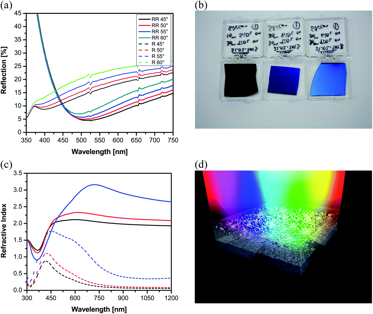 | ||
| Fig. 2 (a) Reflection spectra of 20 nm TiO2 atop of 50 nm SiO2 coated on silicon (solid line) and 50 nm SiO2 on 20 nm TiO2 coated on silicon (dashed line) at different angles of incidence. "RR" and "R" stand for "reverse-Rayleigh" and "Rayleigh" configurations, respectively. (b) True photograph of silicon samples coated with 30 nm TiO2 film atop of (from left to right) 10, 30 and 50 nm SiO2 films, respectively. (c) Complex refractive index of the Ag–SiO2 nanocomposite with 15% (black), 20% (red) and 40% (blue) filling factors. Solid and dotted-lines represent the real and imaginary parts of RI, correspondingly. (d) Geometry of the anti-Rayleigh hybrid ARC which is composed of the 20 nm nanocomposite atop of SiO2 coated silicon. | ||
The more pronounced reflection drop and red-shift of the curve in reverse-Rayleigh compared to the Rayleigh configuration can be well explained by interference.37 In principle, destructive interference of the direct reflected light and the light reflected at consecutive interfaces requires a phase accumulation of π by the wave traversing the layers back and forth. This easily explains the dogma on using quarter wavelength layers with a small RI as the first (top) layer. However, in the case of a top-film with high RI (reverse-Rayleigh), the light which travels through the low RI layer and the reflected wave have a π phase difference38 which ends up with a destructive interference. In other words, in the case of a top-film with high RI, π phase accumulation comes for free as the impinging light reflected at the various interfaces experiences π–0–π phase shifts. The phase difference of the incoming and reflected light in the cavity is39 where n and d are the RI and thickness of the spacer layer, respectively. By inserting the values of thickness and RI of SiO2 in the mentioned equation, it ends up with
  , which provides the condition of destructive interference. Color changes of the coating by changing the thickness of the spacer layer (i.e. SiO2 film) from 10 to 50 nm, further prove the interference role in the reverse-Rayleigh coating. Fig. 2b shows the true color photograph of the silicon samples coated with 30 nm TiO2 film atop of 10, 30 and 50 nm SiO2 on the silicon substrate.
Nevertheless, neither ARC based on reverse-Rayleigh concept nor Rayleigh provide the desired properties of a wide-band ARC (i.e. whole solar spectrum range) owing to high reflection that appears at short and long wavelengths of the visible for both configurations. Additionally, for shifting the reflection dip to NIR, increasing the layer thickness and/or using a high RI material is needed. Note that there are only a limited number of materials with high refractive index which could fulfill the required RI contrast for the reverse-Rayleigh configuration.
In our opinion, and from technological point of view, the field is revolutionized if a coating is used that would enable both Rayleigh and reverse-Rayleigh configurations simultaneously, at different wavelengths though. Suppressing the reflections at multiple wavelengths would automatically enable a broadband ARC based on ultrathin films. However, this requires the use of strongly dispersive materials in the design of the ARC. Ideally, the geometrical dispersion that degrades the anti-reflection action beyond the target wavelength in an ARC design where non-dispersive materials are used has to be compensated by a suitable material dispersion. This perfect balancing, however, requires an anomalous dispersion in the material properties, which is always accompanied by absorption. Nonetheless, motivated by the recent work on ARC coatings on metals using weakly absorbing materials,29 we may conclude that if the ARC coating is sufficiently thin and contains ultrafine plasmonic nanoparticles, the absorption might not be detrimental. To evaluate the potential of this idea, we sought out a way to design a new concept for a coating that considers artificial materials (metamaterial) in their design that possesses a strong chromatic anomalous dispersion.
Accordingly, we consider a plasmonic nanocomposite of tiny metallic nanoparticles embedded in a dielectric host as a metamaterial with the required highly dispersive refractive index. The properties of the nanocomposite can be tuned by many parameters which constitute a great degree of freedom. They constitute an extraordinary material platform with many intriguing advantages. The fabrication of these nanocomposites is based on self-assembly processes using sputter techniques, which is well established,40–42 and they can be deposited on a large surface in a short time and at low costs (for more details see the Methods section).
This metamaterial derives its unique properties from the excitation of localized plasmon polaritons in the metallic nanoparticles.43 The nanoparticles are sufficiently small and arranged sufficiently dense, such that the material can be considered as effectively homogenous and isotropic. The material is characterized by a Lorentzian resonance in the effective permittivity which is centered at the plasmon resonance wavelength. Due to the isotropy of the material and the vanishing of any magnetic response, the permittivity uniquely defines the effective refractive index. The material can be perceived as a strongly dispersive dielectric with some finite absorption in resonance.
It is known that, with filling fractions for the metallic nanoparticles between 20% and 40%, the effective properties cannot be derived from canonical effective medium theories such as Clausius–Mossotti.44 Instead, we used finite-difference time-domain (FDTD) simulations of a sufficiently large super-cell and calculated the dispersive complex reflection and transmission coefficient45 (cf. Methods section). From these coefficients effective properties were retrieved for the composite. These parameters were afterwards fueled into a thin-film transfer matrix technique to simulate all quantities of interest. Selected configurations were equally simulated by the FDTD method to cross-check the predictive power of the effective properties. Identical results were always predicted, justifying the treatment of the nanocomposite as an effective medium (for more details see the Methods section). The dispersive RIs of the nanocomposites with different filling factors are shown in Fig. 2c. It is apparent from this dispersion graph that at resonance the absorption is maximal and the real part of the RI undergoes anomalous dispersion. At wavelengths longer than the resonance wavelength the material is characterized by a large RI (large permittivity) and hence would be suitable to serve in the reverse-Rayleigh configuration as the top material (ntop > nspacer). In contrast, at wavelengths smaller than the resonance wavelength, the medium is characterized by a rather small RI (small permittivity) and accordingly would be appropriate to be used in the Rayleigh configuration as the top material (ntop < nspacer). Therefore, plasmonic nanocomposites can be considered as the hybrid ARC that meets the condition of both Rayleigh and reverse-Rayleigh geometries resulting in a broad-band ARC coating.
We demonstrate the hybrid concept by coating a polished silicon wafer with a 20 nm silver–silicon dioxide nanocomposite separated from the substrate by a thin layer (50 nm) of silicon dioxide as shown schematically in Fig. 2d. Such a stack gives rise to the realization of a black silicon with a homogeneous ultrathin layer coating. Fig. 3a shows the reflection spectra of 20% and 30% nanocomposites deposited on 50 nm SiO2 coated silicon and the inset is the true color photograph of the sample with 30%, which looks black indeed.
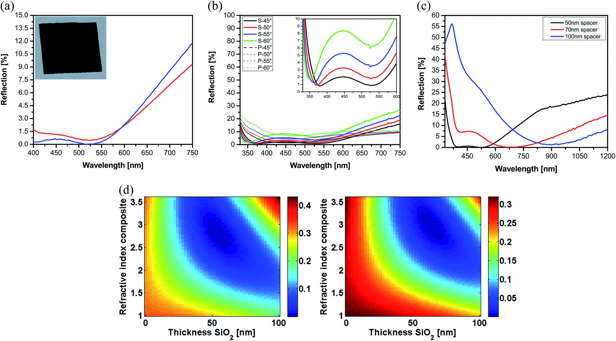 | ||
| Fig. 3 (a) Reflection spectra of 20 nm Ag–SiO2 with 20% (red) and 30% (blue) filling factors deposited atop of 50 nm SiO2 coated silicon. The inset shows the true color photograph of the silicon coated with the optimized film, which turns black in its appearance. (b) Reflection spectra of the film as in Fig. 2c measured at different angles of incidence with s-(solid lines) and p-polarization (dotted lines), (c) reflection spectra of hybrid ARC with 30% filling fraction of metal in the top layer deposited on spacer layers with three different thicknesses. The ARC is deposited again on silicon. Black, red and blue curves showing the spectra of 50, 70 and 100 nm thick spacer layers, correspondingly. (d) Reflection contour of the 20 nm film with various RIs on the SiO2 film with different thicknesses at (left) 800 nm and (right) 900 nm wavelengths. | ||
Angular reflectance measurement of the coating with 30% filling factor (Fig. 3b) shows the marginal angular and polarization dependency of the plasmonic hybrid ARC.46 More details on the angular behavior,33 especially for the angular domain that is not shown here, can be found in the literature.26
The spectra possess two main dips in the reflection spectra. The small wavelength dip is attributed to the graded AR (i.e. in analogue to a configuration where 50 nm SiO2 is deposited atop of 20 nm TiO2 (cf.Fig. 1d (inset))) and the second reflection dip originates from the destructive interference of the reflected field (i.e. in analogy with the TiO2 film atop of SiO2 (cf.Fig. 1d (black curve))).
In spite of the expected wavelength shifts of the antireflection dips [cf.Fig. 3b (inset)], one peak at 450 nm (i.e. where the plasmon of the nanocomposite arise) is also revealed that is invariant against the angle of incidence and hence we attribute it to the plasmon resonance of the composite. Indeed, the wavelength of the peak remains unchanged by angle variation, which confirms the localized nature of the (particle plasmon) resonance.
To demonstrate the tunability of the hybrid ARC coating and meanwhile to gain more understanding about the role of plasmon in the observed phenomena, the effect of the spacer layer on the optical responses was examined. Keeping the top layer thickness and composition constant while increasing the thickness of SiO2 from 50 nm to 100 nm, a red-shift of the reverse-Rayleigh as well as Rayleigh antireflection dips was observed (Fig. 3c). This behavior is in good agreement with our simulation (Fig. 3d) which shows that an increase of the spacer results in a broad ARC in NIR (800–900 nm) for the case of the reverse-Rayleigh configuration. On the other hand, ARC performance of the graded configuration (small wavelength regime) in the hybrid is deteriorated by thickening the spacer layer. Indeed, the origin of the mentioned high reflection with a thicker inter-layer could be attributed to two phenomena; firstly the constructive interference of the incident and the reflected light, and secondly, the spectral overlap of the plasmonic resonance of the nanocomposite and the Rayleigh antireflection dip. Such an overlap occurred because of the red-shift of the Rayleigh originated dip via thickening of the spacer layer.
Indeed, integrating the plasmonic structure as a hybrid ARC coating provides an additional degree of freedom for tuning the performance of the ARC coating. In other words, by using the hybrid plasmonic ARC, the designer can reach the desired optical properties not only by alteration of the layer thickness but also by adjusting the filling factor (RI) and type of the metallic constituents of the nanocomposite. Generally, the performance of the hybrid ARC depends on the contrast of the RIs between the layers. At the wavelengths where the top layer shows higher RI, the reverse-Rayleigh condition is satisfied but the traditional Rayleigh would be realized once the top film possesses the lower RI in the stack. The presented plasmonic anti-reflector shows such a low and tunable reflectivity due to the extreme dispersive RI of the metamaterial (cf.Fig. 2c), which has been shown formerly.47–50 The RI of the nanocomposite with 40% filling factor changes from 0.9 up to 3.15 from small to long wavelengths. In other words, the relative RI changes of the host matrix before and after embedding of the nanoparticles can vary from −30% to +140%.
In fact, the tunability of the plasmon resonance and correspondingly the reflection change29 by changing the filling factor of the nanocomposite provide the possibility for the coloring of metals using our hybrid concept. Fig. 4a shows a true photograph of samples of 25 nm SiO2 coated gold film which is covered with 20 nm gold–SiO2 nanocomposite with a variety of filling factors, creating a spectrum of colors including yellow, orange, blue and green. The colors originated from the different reflection drops associated with each filling factor demonstrating the potential of the hybrid concept for realization of plasmonic rainbow colors.51 Note that demonstration of various colors on the silicon substrate is not possible under the same conditions (i.e. constant thickness of layers while varying the filling factor). It seems that, the surface plasmon of the gold film (which is absent on silicon) in parallel with the hybrid ARC contributes to the rainbow colors.
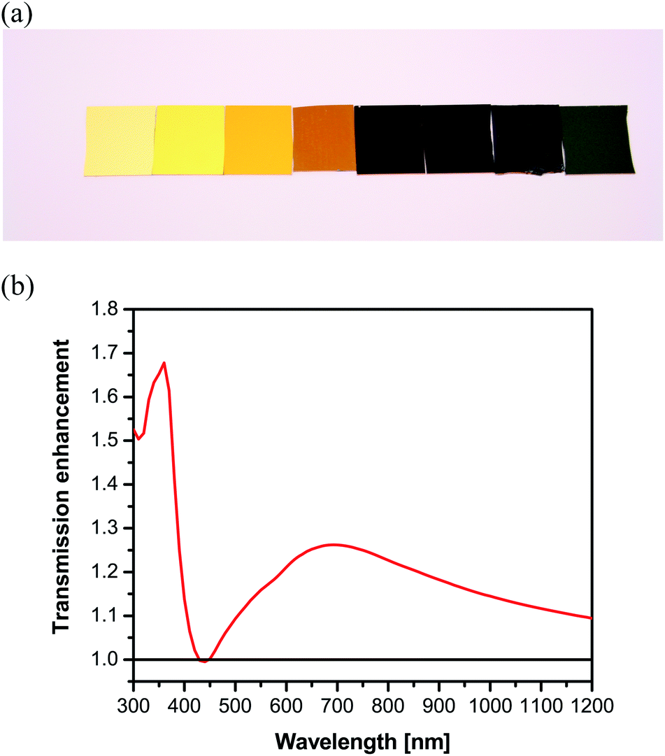 | ||
| Fig. 4 (a) True photograph of 25 nm SiO2 coated gold film covered by 20 nm Au–SiO2 nanocomposite with different filling factors. From left to right the filling factor of the nanocomposite increased (13%, 20%, 30%, 40%, 50% and 60%, correspondingly) while the first and second samples are bare gold and 45 nm SiO2 coated gold, respectively. (b) Calculated transmission enhancement of silicon by plasmonic coating, which is calculated by normalization of the transmission of coated silicon by that of the bare one. The black line shows the normalized transmission of bare silicon while the red curve is the normalized transmission of the Ag–SiO2 nanocomposite deposited on SiO2 coated silicon. | ||
We believe that the hybrid concept could pave the way for new highly efficient ARCs for a variety of applications ranging from photovoltaics52 and optics to solar absorbers and stealth technology53,54 as well as other fields where high reflection is undesired. But for energy applications, not only the low reflectance rather high transmission is desired. Calculation showed that the light transmission into the substrate (silicon) is enhanced by using the plasmonic coating. Fig. 4b shows the light absorbed by silicon (i.e. light transmitted into silicon) by means of current plasmonic coating. The light reaching the substrate is apparently increased through the coating, which shows the potential of such an approach for energy harvesting purposes. However, the preliminary results on photocurrent measurements of presented coating on p-silicon showed some current loss that we attributed to the poor interface of the prepared films which acts as the sites for electron–hole recombination. Nevertheless, a more sophisticated design is required to better explore the role of the present ARC for electron–hole generation which is beyond the scope of this manuscript.
Conclusions
In summary, we demonstrated a new concept for antireflection coatings and experimentally showed an ultra-thin tunable plasmonic anti-reflector by using a routine technique of MEMS/NEMS technology. The developed hybrid ARC, which is based on a continuous plasmonic medium, acts as a consolidation of the graded-index and interferometer (reverse-Rayleigh) providing a wide-band reflection drop throughout the visible spectrum. Due to the simplicity of our production approach, the concept can be further extended to other substrates/applications where broadband ultra-thin anti-reflective coatings are required.Methods
Fabrication
All depositions were carried out in a cylindrical vacuum chamber, which was primarily evacuated to 10−6 mbar. We used an RF magnetron for sputtering of SiO2 and a DC magnetron sputter source for silver and gold. Both sources were oriented in reverse directions relative to the sample holder at 50° angle to the substrate plane. All the coating was done while the rotatable sample holder was spinning in order to end up with a uniform thickness and composition (details in ref. 40–42). In order to keep the filling factor below the percolation threshold, the deposition rate of the metal was adjusted to be less than that of the dielectric during co-deposition. In other words, to avoid the coalesce of nanoparticles in the matrix, i.e. the formation of fractal aggregates of NPs, the deposition rate of SiO2 was set to be 10 nm s−1 while the rate of silver was adjusted to be around 3 nm s−1. However, for the creation of the plasmonic rainbow, the mentioned constrain was actually not necessary. Therefore, the gold deposition rate was varied between 3 and 13 nm s−1. This enabled us to fabricate a gold nanocomposite with a wider range of filling factors (below and above the percolation threshold). Nevertheless, we increased the rate of deposited gold only to an extent such that we avoid the formation of a continuous gold film instead of particles. By formation of a gold film no localized plasmon resonance would appear which has to be avoided. From the final TEM investigation data we could eventually observe that the particles do not coalesce and they are mainly spherical which further simplified the theoretical modeling (see Simulation).The thickness of the films was measured with a profilometer (Dektak 8000 surface profile measuring system) and the thickness of dielectric was further measured with an ellipsometer (M2000 (J.A. Woollam Co., Inc.)). Optical properties of the samples at normal incidence were measured with a UV/vis/NIR spectrometer (Lambda900, Perkin Elmer). For transmission measurements, the base line was collected by measuring the empty compartment (i.e. air considered as the reference) while for reflection measurements, the mirror provided by the company was used. To extract the absolute value of reflection, the measured reflection spectra of the samples were normalized to the tabulated data of the mirror provided by the manufacturing company (PerkinElmer). In all types of measurements, the scan step was fixed to 4 nm and the base line was collected twice by a full sweep across the spectral domain of interest while the integration and acquisition times were kept constant.
Polarization-dependent and variable angle spectroscopic Ellipsometry reflection measurements of the films was carried out with J.A. Woollam Co., Inc. M2000 UI (spectroscopic ellipsometer) with a dual lamp system with deuterium and Quartz Tungsten Halogen (QTH) lamps as light sources (data provided by LOT catalogue Europe). The angle sweep step was selected to be 5° or 10° and the angle variation from 45° to 85° was performed. In order to have a comparable study and achieve the best signal-to-noise, 5 second acquisition time was applied for all experiments. Accordingly, the measurement did not take more than few seconds. For analyzing the data, CompleteEASE® software package provided by the company was used.
Simulations
FDTD simulations were made with an in-house developed code on a sufficiently large cluster.45 The simulated structure compares entirely to the experimental geometry. For this purpose a random arrangement of spherical metallic nanoparticles with a diameter corresponding to the mean diameter as extracted from the TEM samples has been generated. The filling fraction has been adjusted according to the experimental values and we only enforced an isolation of all spherical nanoparticles, i.e. their interpenetration has been excluded. The spatial domain considered in the simulation was 100 nm × 100 nm in lateral directions. In these directions periodic boundaries were enforced to eventually mimic an infinitely extended space. The chosen spatial domain was sufficiently large to exclude any notable effect from the periodicity. In the propagation direction the sequence of layers and their respective thicknesses have been considered in full analogy with the experimental situations. Permittivity of SiO2 has been taken as non-dispersive and equal to 2.25. Permittivity of gold was taken as tabulated in the literature55 but with an additional correction term to accommodate the finite and small size of the nanoparticles.56 The intrinsic dispersion of the material has been fully taken into account by performing at each wavelength an individual simulation and adjusting the free parameters in a Drude model to provide a material with the respective properties at the considered wavelength. Spatial discretization in the FDTD was 1 nm and perfectly matched layers were used in the propagation direction. To retrieve the effective properties the complex reflection and transmission coefficients have been extracted from the FDTD simulations and a parameter retrieval has been applied.57Acknowledgements
M.K.H., F.F. and M.E. gratefully acknowledge the financial support by the German Research Foundation (DFG) through the projects EL 554/1-1 and SFB 677 (C1,C9). M.E. would like to thank the Initiative and Networking Fund of the Helmholtz Association (grant no. VH-NG-523) for providing the financial base for the start-up of his research group. The authors also gratefully acknowledge Dr U. Schürmann and Prof. Kienle for TEM measurements. This work was supported by the German Federal Ministry of Education and Research (PhoNa) and by the Thuringian State Government (MeMa). We thank Karsten Verch (http://www.karstenverch.com) for his artistic view of the concept in Fig. 2d.Notes and references
- D. Bouhafs, A. Moussi, A. Chikouche and J. Ruiz, Design and simulation of antireflection coating systems for optoelectronic devices: Application to silicon solar cells, Sol. Energy Mater. Sol. Cells, 1998, 52, 79–93 CrossRef CAS.
- L. Rayleigh, On reflection of vibrations at the confines of two media between which the transition is gradual, Proc. Lond. Math. Soc., 1879, 1, 51–56 CrossRef.
- J. Cox, G. Hass and A. Thelen, Triple-layer antireflection coatings on glass for the visible and near infrared, J. Opt. Soc. Am., 1962, 52, 965–968 CrossRef CAS.
- A. Turner, Some current developments in multilayer optical films, J. Phys. Radium, 1950, 11, 444–460 CrossRef.
- W. Lowdermilk and D. Milam, Graded-index antireflection surfaces for high-power laser applications, Appl. Phys. Lett., 1980, 36, 891–893 CrossRef CAS PubMed.
- J.-Q. Xi, et al. Optical thin-film materials with low refractive index for broadband elimination of Fresnel reflection, Nat. Photonics, 2007, 1, 176–179 CAS.
- S. Mukherjee and W. Lowdermilk, Gel-derived single layer antireflection films, J. Non-Cryst. Solids, 1982, 48, 177–184 CrossRef CAS.
- M. Minot, The angular reflectance of single-layer gradient refractive-index films, J. Opt. Soc. Am., 1977, 67, 1046–1050 CrossRef CAS.
- P. Clapham and M. Hutley, Reduction of lens reflexion by the “Moth Eye” principle, Nature, 1973, 244, 281–282 CrossRef.
- Y.-F. Huang, et al. Improved broadband and quasi-omnidirectional anti-reflection properties with biomimetic silicon nanostructures, Nat. Nanotechnol., 2007, 2, 770–774 CrossRef CAS PubMed.
- R. Peterson and J. Ramsey, Thin film coatings in solar-thermal power systems, J. Vac. Sci. Technol., 1975, 12, 174–181 CrossRef CAS.
- J. Zhao and M. A. Green, Optimized antireflection coatings for high-efficiency silicon solar cells, IEEE Trans. Electron Devices, 1991, 38, 1925–1934 CrossRef CAS.
- J. K. Kim, et al. Light extraction enhancement of GaInN light emitting diodes by graded refractive index Indium Tin Oxide anti reflection contact, Adv Mater., 2008, 20, 801–804 CrossRef CAS.
- P. Spinelli, M. Verschuuren and A. Polman, Broadband omnidirectional antireflection coating based on subwavelength surface Mie resonators, Nat. Commun., 2012, 3, 692 CrossRef CAS PubMed.
- Y. Wang, Y. Liu, H. Liang, Z. Mei and X. Du, Broadband antireflection on the silicon surface realized by Ag nanoparticle-patterned black silicon, Phys. Chem. Chem. Phys., 2013, 15, 2345–2350 RSC.
- A. Kabiri, F. Capasso and E. Girgis, Buried Nanoantenna Arrays: Versatile Antireflection Coating, Nano Lett., 2013, 13(12), 6040–6047 CrossRef CAS PubMed.
- P. Spinelli, et al. Optical impedance matching using coupled plasmonic nanoparticle arrays, Nano Lett., 2011, 11, 1760–1765 CrossRef CAS PubMed.
- X.-R. Huang, R.-W. Peng and R.-H. Fan, Making metals transparent for white light by spoof surface plasmons, Phys. Rev. Lett., 2010, 105, 243901 CrossRef.
- R.-H. Fan, et al. Broadband antireflection and light-trapping enhancement of plasmonic solar cells, Phys. Rev. B: Condens. Matter Mater. Phys., 2013, 87, 195444 CrossRef.
- D. M. Braun and R. L. Jungerman, Broadband multilayer antireflection coating for semiconductor laser facets, Opt. Lett., 1995, 20, 1154–1156 CrossRef CAS.
- B. Moys, The theory of double-layer antireflection coatings, Thin Solid Films, 1974, 21, 145–157 CrossRef.
- Y. Fink, et al., A dielectric omnidirectional reflector, Science, 1998, 282, 1679–1682 CrossRef CAS.
- M. F. Schubert, J.-Q. Xi, J. K. Kim and E. F. Schubert, Distributed Bragg reflector consisting of high-and low-refractive-index thin film layers made of the same material, Appl. Phys. Lett., 2007, 90, 141115–141113 CrossRef PubMed.
- M. Ettenberg, A new dielectric facet reflector for semiconductor lasers, Appl. Phys. Lett., 1978, 32, 724 CrossRef CAS PubMed.
- H.-T. Chen, Interference theory of metamaterial perfect absorbers, Opt. Express, 2012, 20, 7165–7172 CrossRef PubMed.
- M. K. Hedayati, et al. Design of a perfect black absorber at visible frequencies using plasmonic metamaterials, Adv Mater., 2011, 23, 5410–5414 CrossRef CAS PubMed.
- M. K. Hedayati, F. Faupel and M. Elbahri, Tunable broadband plasmonic perfect absorber at visible frequency, Appl. Phys. A: Mater. Sci. Process., 2012, 109, 769–773 CrossRef CAS.
- M. A. Kats, et al. Ultra-thin perfect absorber employing a tunable phase change material, Appl. Phys. Lett., 2012, 101, 221101–221105 CrossRef PubMed.
- M. A. Kats, R. Blanchard, P. Genevet and F. Capasso, Nanometre optical coatings based on strong interference effects in highly absorbing media, Nat. Mater., 2012, 12, 20–24 CrossRef PubMed.
- X. Xiong, S. C. Jiang, Y. H. Hu, R. W. Peng and M. Wang, Structured metal film as a perfect absorber, Adv Mater., 2013, 25, 3994–4000 CrossRef CAS PubMed.
- J. Hao, et al. High performance optical absorber based on a plasmonic metamaterial, Appl. Phys. Lett., 2010, 96, 251104 CrossRef PubMed.
- N. Liu, M. Mesch, T. Weiss, M. Hentschel and H. Giessen, Infrared perfect absorber and its application as plasmonic sensor, Nano Lett., 2010, 10, 2342–2348 CrossRef CAS PubMed.
- M. Hedayati, A. Zillohu, T. Strunskus, F. Faupel and M. Elbahri, Plasmonic tunable metamaterial absorber as ultraviolet protection film, Appl. Phys. Lett., 2014, 104, 041103 CrossRef PubMed.
- M. K. Hedayati, F. Faupel and M. Elbahri, Review of Plasmonic Nanocomposite Metamaterial Absorber, Materials, 2014, 7(2), 1221–1248, DOI:10.3390/ma7021221.
- E. T. Hamden, et al., Ultraviolet antireflection coatings for use in silicon detector design, Appl. Opt., 2011, 50, 4180–4188 CrossRef CAS PubMed.
- M. Radecka, K. Zakrzewska, H. Czternastek, T. Stapiński and S. Debrus, The influence of thermal annealing on the structural, electrical and optical properties of TiO2−x thin films, Appl. Surf. Sci., 1993, 65–66, 227–234, DOI:10.1016/0169-4332(93)90663-V.
- H.-T. Chen, et al. Antireflection coating using metamaterials and identification of its mechanism, Phys. Rev. Lett., 2010, 105, 073901 CrossRef.
- D. L. Caballero, A theoretical development of exact solution of reflectance of multiple layer optical coatings, J. Opt. Soc. Am., 1947, 37, 176–178 CrossRef CAS.
- K. Renk and L. Genzel, Interference filters and Fabry-Perot interferometers for the far infrared, Appl. Opt., 1962, 1, 643–648 CrossRef CAS.
- F. Faupel, V. Zaporojtchenko, T. Strunskus and M. Elbahri, Metal polymer nanocomposites for functional applications, Adv. Eng. Mater., 2010, 12, 1177–1190 CrossRef CAS.
- U. Schürmann, W. Hartung, H. Takele, V. Zaporojtchenko and F. Faupel, Controlled syntheses of Ag–polytetrafluoroethylene nanocomposite thin films by co-sputtering from two magnetron sources, Nanotechnology, 2005, 16, 1078 CrossRef.
- H. Takele, H. Greve, C. Pochstein, V. Zaporojtchenko and F. Faupel, Plasmonic properties of Ag nanoclusters in various polymer matrices, Nanotechnology, 2006, 17, 3499 CrossRef CAS PubMed.
- S. A. Maier, Plasmonics: Fundamentals and Applications, Springer, 2007 Search PubMed.
- T. C. Choy, Effective Medium Theory: Principles and Applications, Oxford University Press, 1999, vol. 102 Search PubMed.
- A. Taflove and S. C. Hagness, Computational Electrodynamics: the Finite-difference Time-domain Method, Artech House, Incorporated, 2005 Search PubMed.
- C. Etrich, et al., Effective Optical Properties of Plasmonic Nanocomposites, Materials, 2014, 7, 727–741 CrossRef PubMed.
- U. Schürmann, Eigenschaften von Polymer-Silber-Nanokompositen hergestellt durch Co-Sputtern, PhD thesis, University of Kiel, 2006.
- J. De Sande, et al., Refractive index of Ag nanocrystals composite films in the neighborhood of the surface plasmon resonance, J. Appl. Phys., 2002, 91, 1536–1541 CrossRef CAS PubMed.
- S. G. Moiseev, Composite medium with silver nanoparticles as an anti-reflection optical coating, Appl. Phys. A: Mater. Sci. Process., 2011, 103, 619–622 CrossRef CAS.
- S. Dutta Gupta, Strong-interaction—mediated critical coupling at two distinct frequencies, Opt. Lett., 2007, 32, 1483–1485 CrossRef.
- T. Huang and X.-H. N. Xu, Synthesis and characterization of tunable rainbow colored colloidal silver nanoparticles using single-nanoparticle plasmonic microscopy and spectroscopy, J. Mater. Chem., 2010, 20, 9867–9876 RSC.
- S. Pillai, K. Catchpole, T. Trupke and M. Green, Surface plasmon enhanced silicon solar cells., J. Appl. Phys., 2007, 101, 093105 CrossRef PubMed.
- J.-B. Brückner, et al., Metamaterial filters at optical-infrared frequencies, Opt. Express, 2013, 21, 16992–17006 CrossRef PubMed.
- N. Engheta, in Antennas and Propagation Society International Symposium, 2002, IEEE. 392–395 (IEEE) Search PubMed.
- P. B. Johnson and R.-W. Christy, Optical constants of the noble metals, Phys. Rev. B: Solid State, 1972, 6, 4370 CrossRef CAS.
- S. Kawata, Near-field Optics and Surface Plasmon Polaritons, Springer, 2001, vol. 81, p. 210 Search PubMed.
- C. Menzel, C. Rockstuhl, T. Paul, F. Lederer and T. Pertsch, Retrieving effective parameters for metamaterials at oblique incidence, Phys. Rev. B: Condens. Matter Mater. Phys., 2008, 77, 195328 CrossRef.
| This journal is © The Royal Society of Chemistry 2014 |