 Open Access Article
 This Open Access Article is licensed under a Creative Commons Attribution-Non Commercial 3.0 Unported Licence
Single inorganic–organic hybrid nanowires with ambipolar photoresponse†
Jewon
Yoo
,
Jaeyeon
Pyo
and
Jung Ho
Je
*
X-ray Imaging Center, Department of Materials Science and Engineering, Pohang University of Science and Technology, Pohang, 790-784, Republic of Korea. E-mail: jhje@postech.ac.kr
First published on 5th March 2014
Abstract
We report for the first time single nanowires (NWs) with ambipolar (positive/negative) photoresponse that changes sign depending on the illumination wavelength. The single NWs were grown by the meniscus-guided method using inorganic (ZnO nanoparticles)–organic (PEDOT:PSS) hybrid materials. The ambipolar photoresponse of the single NWs enabled us to develop an unprecedented spectrum-discriminating NW photodetector array.
Optoelectronic devices1 have attracted great attention in various domains of photonics including light generation, propagation, detection, and modulation. In particular, NW optoelectronic devices based on photoconducting properties such as NW photodetectors2,3 and NW optical switches4,5 are essential elements for important applications such as optical communications and optical interconnects in nanophotonic circuits.6 In traditional photoconductors,7 positive photoresponse is generally observed by generating mobile charge carriers in the valence and/or conduction bands under light illumination.8 Ambipolar (positive/negative) photoresponse that changes sign depending on the illumination wavelength9–11 or external stimuli12–14 has recently emerged for multifunctional optoelectronic devices such as “light-gated” transistors,15 mirror photoswitches16 and logic-controllable hybrid devices.17 Ambipolar photoresponse is, however, largely unexplored in single NWs that are recognized as one of the essential building blocks for nanophotonics.18 Furthermore it remains a challenge to directly integrate single NWs in the designed positions19 despite recent developments of flow-assisted alignment,20 Langmuir–Blodgett approach,21 and microcontact printing.22 In this study, we report the development of single NWs with ambipolar photoresponse based on inorganic–organic hybrid materials. We also demonstrate a novel NW photodetector array of single inorganic–organic hybrid NWs, integrated at the planned sites.
Here, blend solutions of n-type ZnO NPs23 and p-type poly(3,4-ethylenedioxythiophene):poly(styrenesulfonate) (PEDOT:PSS)24 prepared in water were used to grow inorganic–organic hybrid NWs. Single ZnO NP–PEDOT:PSS hybrid NWs were produced by the meniscus-guided method25,26 using the blend solutions of ZnO NPs and PEDOT:PSS. The single hybrid NWs showed ambipolar photoresponse depending on the illumination wavelength. Individual growth of the single hybrid NWs at the planned sites was performed for a spectrum (UV-visible)-discriminating photodetector array. We believe that single NWs with ambipolar photoresponse will open up a novel route to design new functional nanodevices for advanced optoelectronic applications.
Fig. 1(a) schematically illustrates the growth of ZnO NP–PEDOT:PSS hybrid NWs. When a micropipette touches the substrate, a meniscus of the blend solution is created at its opening. As the micropipette (radius r0 ∼ 0.6 μm) is pulled away, the meniscus is stretched, its cross-section decreases down to the nanoscale, and the solvent (water) evaporates,26 yielding a hybrid NW. As the pulling continues, a freestanding, high-aspect-ratio hybrid NW is grown. The wire radius, r, can be accurately controlled by tuning the pulling speed, v (Fig. S1, ESI†). The top schematic of Fig. 1(b) shows meniscus-guided direct writing of the hybrid NWs by manipulating the micropipette using a three-axis, motion-controlled stage. To form a connected NW, we move the suspended end of the freestanding NW down to the second electrode, with the nozzle end in close proximity so that the meniscus under the nozzle extends to immerse both the NW end and the region of contact on the second electrode. Then, the micropipette is rapidly withdrawn to form the second bond.
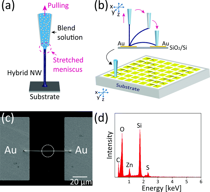 | ||
| Fig. 1 Growth of ZnO NP–PEDOT:PSS hybrid NWs. (a) Scheme of hybrid NW growth by pulling a micropipette filled with a ZnO NP–PEDOT:PSS blend solution. (b) Scheme of the precise integration of single hybrid NWs at the planned sites by meniscus-guided direct writing. (c) FE-SEM image of single hybrid NWs on Au electrodes. (d) EDS spectrum of a region (white dashed circle) of the single hybrid NW in (c). | ||
Furthermore, we are able to precisely integrate single hybrid NWs at the planned sites by individually manipulating the micropipette and the substrate using two three-axis, motion-controlled stages (accuracy: 250 nm), as schematically illustrated in the bottom of Fig. 1(b). The field emission scanning electron microscopy (FE-SEM) image of Fig. 1(c) shows a single hybrid NW (r ∼ 250 nm and l (length) ∼ 75 μm) integrated on Au electrodes. The energy-dispersive X-ray spectroscopy (EDS) spectrum in Fig. 1(d), taken from a region (white dashed circle) of the single hybrid NW, indicates the presence of C, O, Zn, and S elements (the Si peak and most of the O peaks come from the SiO2/Si substrate) from PEDOT:PSS and ZnO NPs.
The photoresponse of single hybrid NWs was dependent on ZnO NP concentration. Single hybrid NWs (r ∼ 250 nm, l ∼ 75 μm) with various ZnO NP concentrations (0 to 50 wt%) were prepared onto pre-designed Au electrodes (inset of Fig. 2(a)). Their photoconducting properties were then measured using a two-probe method under UV (λ = 300–400 nm; 0.19 mW cm−2) or visible (λ = 400–700 nm; 2.87 mW cm−2) light illumination. All the single hybrid NWs showed ohmic behavior,27 as clearly demonstrated in their I–V curves (Fig. S2, ESI†). Fig. 2 shows typical variations in the relative current densities, Δj, recorded for three representative single NWs of (a) PEDOT:PSS, (b) 20 wt% ZnO NP–PEDOT:PSS, and (c) 30 wt% ZnO NP–PEDOT:PSS, periodically exposed to UV (or visible) light. Here Δj is defined as:
| Δj ≡ (jill − j0)/j0 | (1) |
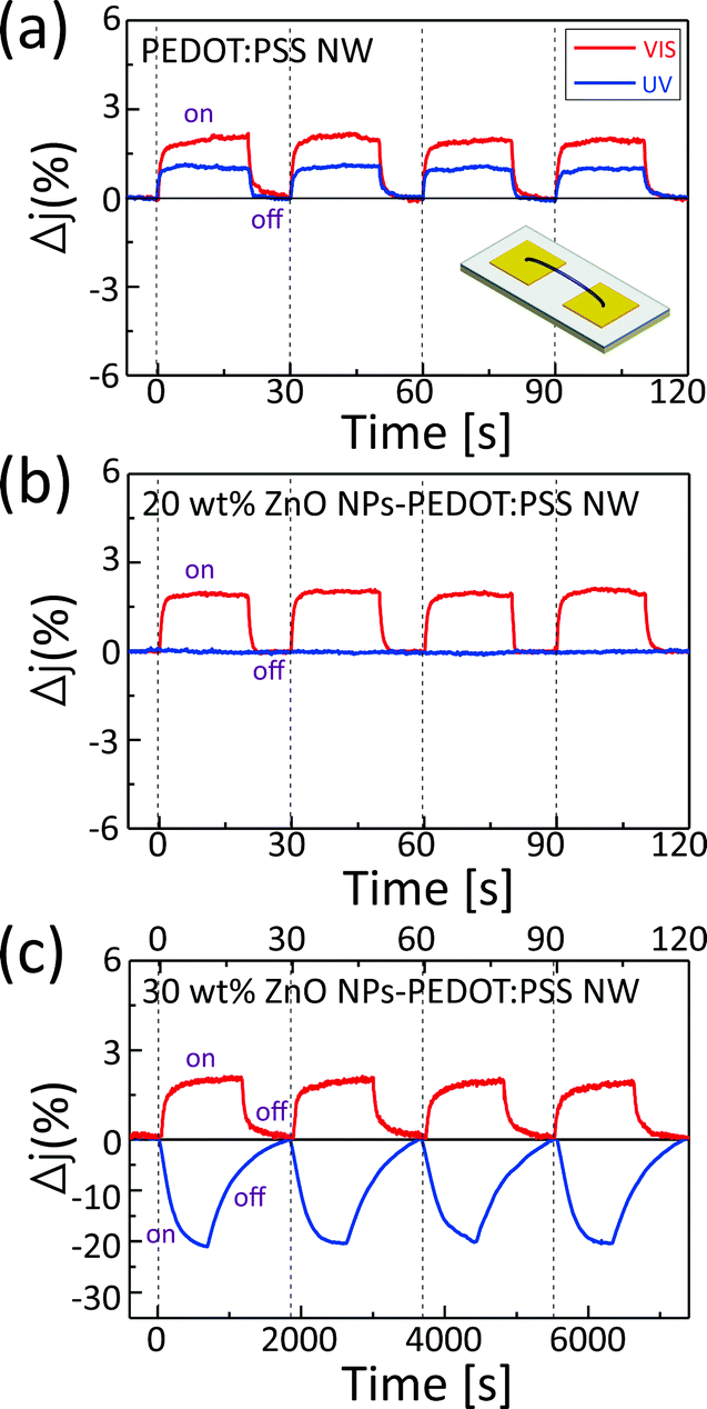 | ||
| Fig. 2 Typical variations in relative current densities, Δj, recorded for three representative single NWs of (a) PEDOT:PSS, (b) 20 wt% ZnO NP–PEDOT:PSS, and (c) 30 wt% ZnO NP–PEDOT:PSS, periodically exposed to UV (or visible) light. The measurements were conducted under ambient conditions at 1 V bias. | ||
The photoresponse of the hybrid NWs is derived from the carriers of PEDOT:PSS (p-type semiconductor), i.e. holes. Under visible light illumination, electrons in the valence band of PEDOT:PSS with a band-gap energy of 1.6 eV (ref. 28) can be excited into the conduction band (see the energy diagram of Fig. S4(a), ESI†), increasing the hole carriers. This explains the positive photoresponse of the hybrid NWs under visible light illumination regardless of ZnO concentrations (Fig. 2 and S3, ESI†). On the other hand, the excitation of a ZnO NP by UV light illumination produces excited holes and electrons (Fig. S4(b), ESI†). Then, the electrons can be injected into the valence band of PEDOT:PSS (Fig. S4(b), ESI†), which decreases the carrier number of PEDOT:PSS and as a result lowers the current density j of the hybrid NWs (Fig. 2 and S3, ESI†), as suggested.10
To gain insight into the charge transfer, UV-vis absorption and FTIR studies were carried out for ZnO NP–PEDOT:PSS hybrid films that showed similar photoresponse to single hybrid NWs (compare Fig. S3 with Fig. S5, ESI†). Fig. 3(a) shows the UV-vis absorption spectra of the hybrid films as a function of ZnO NP concentration. The absorption at λ ∼ 360 nm (UV regime) is expected from the wide band-gap (3.37 eV) of ZnO.4 The progressive enhancement in absorbance with ZnO NP concentration is consistent with the decrease in Δj under UV light illumination as shown in Fig. S5, ESI.† Here the ZnO NPs were well dispersed in single hybrid NWs, as shown in the transmission electron microscopy (TEM) images (Fig. S6, ESI†). Fig. 3(b) shows difference FTIR spectra of a hybrid film (ZnO NP concentration of 50 wt%) under UV light illumination and in the dark, acquired using the data before UV light irradiation as a baseline. The decreased absorbance at 1290, 1177, 1070, 966, and 829 cm−1 from PEDOT29 and 1004, 1047 and 1132 cm−1 from PSS30 under UV light illumination for 5 min (blue line) is, as suggested,10 attributed to the reduction of PEDOT:PSS by the electron transfer via the excitation of ZnO NPs.10 The gradual increase in the decreased absorbance in the dark (Fig. 3(b)), nearly recovering to its original state within 30 min, corresponds to the oxidation of reduced PEDOT:PSS.10
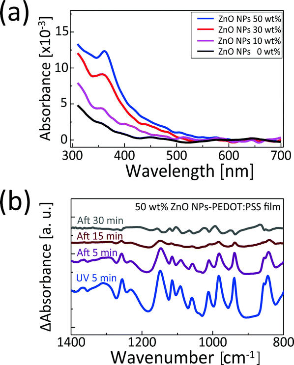 | ||
| Fig. 3 UV-vis absorption and FTIR analyses. (a) UV-vis absorption spectra of ZnO NP–PEDOT:PSS hybrid films on quartz glass. (b) FTIR difference spectra of a 50 wt% ZnO NP–PEDOT:PSS hybrid film on Si wafer. | ||
To demonstrate further the versatility of our approach, we performed individual growth of single hybrid (30 wt% ZnO NP–PEDOT:PSS) NWs with ambipolar photoresponse (Fig. 2(c)) at the planned sites, as schematically illustrated in Fig. 4(a). Fig. 4(b) shows the optical microscopy image of a “heart” pattern of the single hybrid NWs integrated on Au patterned electrodes. The single hybrid NWs were precisely positioned at the planned sites, as demonstrated by FE-SEM images shown in Fig. S7(a) and (b), ESI† for the red and blue box regions in Fig. 4(b), respectively. For each NW in Fig. 4(b), the relative current density Δj under visible (or UV) light illumination was measured (Fig. S8(b), ESI†) and was linearly converted to 8-bit red (or 8-bit blue) color from 0 to 255 with “255” representing the maximum (or the minimum) measured Δj (see eqn (1) and (2) in Fig. S8(c) and Table S1, ESI†), as demonstrated for each NW as a pixel in Fig. 4(c). We were able to discriminate visible and UV light based on the ambipolar photoresponse of the NWs, as displayed in Fig. 4(c) by the red (left) and the blue (right) colors under visible and UV light illumination, respectively. The NW-to-NW variation in Δj was very small, 2.61 ± 0.14% (or −18.91 ± 2.14%) (mean ± SD) for visible (or UV) light, indicating the excellent uniformity of the integrated NWs. Single hybrid NWs with ambipolar photoresponse open an exciting opportunity for the creation of a spectrum-discriminating NW photodetector that can bridge UV photonics31 and visible photonics.32
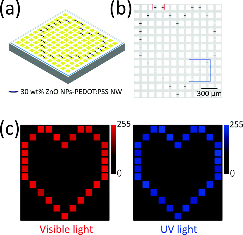 | ||
| Fig. 4 Individual integration of the single hybrid (30 wt% ZnO NP–PEDOT:PSS) NW (r ∼ 250 nm, l ∼ 75 μm) array for a spectrum-discriminating photodetector array. (a and b) Scheme and OM image of a “heart” pattern of the single hybrid NWs on Au patterned electrodes. The red and blue box regions in (b) were observed by FE-SEM (Fig. S7(a) and (b), ESI†), respectively. (c) Ambipolar photoresponse of the single hybrid NW pattern. Each NW, as a pixel, displays 8-bit red (left) (or 8-bit blue (right)) color to which the relative current density Δj was linearly converted under visible (or UV) light illumination. The measurements were conducted under ambient conditions at 1 V bias. | ||
Conclusions
In summary, we developed single ZnO NP–PEDOT:PSS hybrid NWs with ambipolar photoresponse depending on the illumination wavelength, using the meniscus-guided method. Ambipolar photoresponse was realized for the single hybrid NWs at high ZnO NP concentrations (>20 wt%). By individually integrating single hybrid (30 wt% ZnO NP–PEDOT:PSS) NWs at the planned sites, we demonstrated a spectrum-discriminating NW photodetector array that can discriminate UV and visible light. The NW array showed a very small NW-to-NW photoresponse variation (Δj: 2.61 ± 0.14% (or −18.91 ± 2.14%) (mean ± SD) for visible (or UV) light), indicating the excellent uniformity of integrated NWs. We believe that single NWs with ambipolar photoresponse hold a promising route for the development of a variety of optoelectronic nanodevices with unusual functionality.Acknowledgements
This work was supported by the National Research Foundation of Korea (NRF) grant funded by the Korea government (MSIP) (no. 2006-0050683) and FTIR experiments at Pohang Light Source (PLS) were supported in part by MSIP and POSTECH.Notes and references
- H. Sirringhaus, N. Tessler and R. H. Friend, Science, 1998, 280, 1741 CrossRef CAS; F. Bonaccorso, Z. Sun, T. Hasan and A. C. Ferrari, Nat. Photonics, 2010, 4, 611 CrossRef; S. A. Mcdonald, G. Konstrantatos, S. Zhang, P. W. Cyr, E. J. D. Klem, L. Levina and E. H. Sargent, Nat. Mater., 2005, 4, 138 CrossRef PubMed.
- G. A. O'Brien, A. J. Quinn, D. A. Tanner and G. Redmond, Adv. Mater., 2006, 18, 2379 CrossRef CAS.
- N. Mathews, B. Varghese, C. Sun, V. Thavasi, B. P. Andreasson, C. H. Sow, S. Ramakrishnac and S. G. Mhaisalkarn, Nanoscale, 2010, 2, 1984 RSC.
- H. Kind, H. Yan, B. Messer, M. Law and P. Yang, Adv. Mater., 2002, 14, 158 CrossRef CAS.
- C.-H. Hsieh, L.-J. Chou, G.-R. Lin, Y. Bando and D. Golberg, Nano Lett., 2008, 8, 3081 CrossRef CAS PubMed.
- P. Yang, R. Yan and M. Fardy, Nano Lett., 2010, 10, 1529 CrossRef CAS PubMed.
- X. Gong, M. Tong, Y. Xia, W. Cai, J. S. Moon, Y. Cao, G. Yu, C.-L. Shieh, B. Nilsson and A. J. Heeger, Science, 2009, 325, 1665 CrossRef CAS PubMed; Y. Jin, J. Wang, B. Sun, J. C. Blakesley and N. C. Greenham, Nano Lett., 2008, 8, 1649 CrossRef PubMed; X. Xie, S.-Y. Kwok, Z. Lu, Y. Liu, Y. Cao, L. Luo, J. A. Zapien, I. Bello, C.-S. Lee, S.-T. Lee and W. Zhang, Nanoscale, 2012, 4, 2914 RSC; Z. Wang, M. Safdar, C. Jiang and J. He, Nano Lett., 2012, 12, 4715 CrossRef PubMed.
- N. V. Joshi, in Photoconductivity: Art, Science and Technology, ed. M. Dekker, New York, 1990, ch. 1, pp. 1–33 Search PubMed.
- W. Liu, J.-S. Lee and D. V. Talapin, J. Am. Chem. Soc., 2013, 135, 1349 CrossRef CAS PubMed.
- N. Sakai, G. K. Prasad, Y. Ebina, K. Takada and T. Sasaki, Chem. Mater., 2006, 18, 3596 CrossRef CAS.
- S. Yang, J. Gong and Y. Deng, J. Mater. Chem., 2012, 22, 24522 RSC.
- J.-L. Zhu, G. Zhang, J. Wei and J.-L. Sun, Appl. Phys. Lett., 2012, 101, 123117 CrossRef PubMed.
- H. Nakanishi, K. J. M. Bishop, B. Kowalczyk, A. Nitzan, E. A. Weiss, K. V. Tretiakov, M. M. Apodaca, R. Klajn, J. F. Stoddart and B. A. Grzybowski, Nature, 2009, 460, 371 CrossRef CAS PubMed.
- L. Guo, X. Wang, L. Feng, X. Zheng, G. Chen, X. Yang, F. Xu, N. Tang, L. Lu, W. Ge and B. Shen, Appl. Phys. Lett., 2013, 102, 072103 CrossRef PubMed.
- M. Kim, N. S. Safron, C. Huang, M. S. Arnold and P. Gopalan, Nano Lett., 2012, 12, 182 CrossRef CAS PubMed.
- S. Liu, J. Li, Q. Shen, Y. Cao, X. Guo, G. Zhang, C. Feng, J. Zhang, Z. Liu, M. L. Steigerwald, D. Xu and C. Nuckolls, Angew. Chem., Int. Ed., 2009, 48, 4759 CrossRef CAS PubMed.
- C. Jia, H. Li, J. Jiang, J. Wang, H. Chen, D. Cao, J. F. Stoddart and X. Guo, Adv. Mater., 2013, 25, 6752 CrossRef CAS PubMed.
- R. Yan, D. Gargas and P. Yang, Nat. Photonics, 2009, 3, 569 CrossRef CAS; P. J. Pauzauskie and P. Yang, Mater. Today, 2006, 9, 36 CrossRef.
- B. Su, S. Wang, J. Ma, Y. Wu, X. Chen, Y. Song and L. Jiang, Adv. Mater., 2012, 24, 559 CrossRef CAS PubMed.
- Y. Huang, X. Duan, Q. Wei and C. M. Lieber, Science, 2001, 291, 630 CrossRef CAS PubMed.
- P. Yang, Nature, 2003, 425, 243 CrossRef CAS PubMed; A. R. Tao, J. Huang and P. Yang, Acc. Chem. Res., 2008, 41, 1662 CrossRef PubMed.
- J.-H. Ahn, H.-S. Kim, K. J. Lee, S. Jeon, S. J. Kang, Y. Sun, R. G. Nuzzo and J. A. Rogers, Science, 2006, 314, 1754 CrossRef CAS PubMed.
- A. Kudo, H. Yanagi, K. Ueda, H. Hosono, H. Kawazoe and Y. Yano, Appl. Phys. Lett., 1999, 75, 2851 CrossRef CAS PubMed.
- S. Sista, M.-H. Park, Z. Hong, Y. Wu, J. Hou, W. L. Kwan, G. Li and Y. Yang, Adv. Mater., 2010, 22, 380 CrossRef CAS PubMed.
- J. T. Kim, S. K. Seol, J. Pyo, J. S. Lee, J. H. Je and G. Margaritondo, Adv. Mater., 2011, 23, 1968 CrossRef CAS PubMed.
- J. T. Kim, J. Pyo, J. Rho, J.-H. Ahn, J. H. Je and G. Margaritondo, ACS Macro Lett., 2012, 1, 375 CrossRef CAS.
- A. J. Kronemeijer, H. B. Akkerman, T. Kudernac, B. K. van Wees, B. L. Feringa, P. W. M. Blom and B. de Boer, Adv. Mater., 2008, 20, 1467 CrossRef CAS.
- Y. Cao, G. Yu, C. Zhang, R. Menon and A. J. Heeger, Synth. Met., 1997, 87, 171 CrossRef CAS.
- C. Kvarnström, H. Neugebauer, S. Blomquist, H. J. Ahonen, J. Kankare, A. Ivaska and N. S. Sariciftci, Synth. Met., 1999, 101, 66 CrossRef.
- Z.-S. Wang, T. Sasaki, M. Muramatsu, Y. Ebina, T. Tanaka, L. Wang and M. Watanabe, Chem. Mater., 2003, 15, 807 CrossRef CAS.
- D. J. Gargas, M. E. Toimil-Molares and P. Yang, J. Am. Chem. Soc., 2009, 131, 2125 CrossRef CAS PubMed; Q. Zhuang, Z. Yang and J. Kang, Appl. Phys. Lett., 2013, 102, 171601 CrossRef PubMed; H. Wu, Y. Sun, D. Lin, R. Zhang, C. Zhang and W. Pan, Adv. Mater., 2009, 21, 227 CrossRef.
- Z. Liu, L. Yin, H. Ning, Z. Yang., L. Tong and C.-Z. Ning, Nano Lett., 2013, 13, 4945 CrossRef CAS PubMed; M. Law, D. J. Sirbuly, J. C. Johnson, J. Goldberger, R. J. Saykally and P. Yang, Science, 2004, 305, 1269 CrossRef PubMed; T. Zhai, X. Fang, M. Liao, X. Xu, L. Li, B. Liu, Y. Koide, Y. Ma, J. Yao, Y. Bando and D. Golberg, ACS Nano, 2010, 4, 1596 CrossRef PubMed.
Footnote |
| † Electronic supplementary information (ESI) available: Experimental details, wire radius with pulling speed, I–V curves of hybrid NWs, relative current densities of hybrid NWs and films, SEM images, relative current densities, and converted 8-bit color values for the hybrid NW array. See DOI: 10.1039/c3nr05910c |
| This journal is © The Royal Society of Chemistry 2014 |