High-performance BiOBr ultraviolet photodetector fabricated by a green and facile interfacial self-assembly strategy†
Zhikun
Xu
a,
Lei
Han
ab,
Baohua
Lou
ab,
Xiaowei
Zhang
ab and
Shaojun
Dong
*ab
aState Key Laboratory of Electroanalytical Chemistry, Changchun Institute of Applied Chemistry, Chinese Academy of Sciences, Changchun 130022, Jilin, P.R. China. E-mail: dongsj@ciac.jl.cn
bUniversity of Chinese Academy of Sciences, Beijing, 100049, P.R. China
First published on 7th October 2013
Abstract
We have fabricated a BiOBr film for the first time through water–air interfacial self-assembly, which is a green, easily processable and environmentally friendly strategy. Moreover, an ultraviolet photodetector based on the BiOBr film exhibited excellent stability and a fast response time.
Ultraviolet (UV) photodetectors have attracted considerable attention recently due to their potential applications in optical communication, astronomical study, chemical/biological sensing and flame detection.1–6 Conventionally, UV photodetectors are fabricated through complicated methods such as magnetron sputtering, chemical vapor deposition, molecular beam epitaxy and atomic layer deposition which require expensive equipment and time-consuming processes with fairly high cost and high growth temperature, thus limiting their applications.4,7–13 On the other hand, solution-based interfacial self-assembly methods possess many advantages compared to conventional methods in terms of ease of processing, lower fabrication temperature, large-area coverage, variety in substrates and low cost, making them attractive for practical applications.14 Recently, a variety of nanostructures and optoelectronic devices have been fabricated through oil–water interfacial self-assembly strategies. For example, Vanmaekelbergh and co-workers demonstrated that monolayer film of charged gold nanocrystals could be formed at the heptane–water interface upon a slight reduction of the surface charge.15 The as-formed film could be transferred onto various solid substrates. In 2008, Wang and Xia prepared gold nanoparticle thin films through a pentanol–water interfacial self-assembly method.16 During the experiment, they found that a small amount of ethanol or a gentle shaking can accelerate the assembly process. Finally, monolayer films of gold nanoparticles as large as several square centimeters were obtained after heating at 48 °C for 3 h. Recently, Wu, Fang and co-authors presented a ZnO hollow-sphere nanofilm photodetector fabricated through an oil–water interfacial self-assembly method.17 This nanofilm photodetector showed high sensitivity, good stability and a fast response time. In addition, they fabricated another photodetector based on a NiCo2O4 nanofilm assembled at the oil–water interface via the same strategy.18 Although the quality of these nanofilms formed at the oil–water interface is good, some disadvantages still exist in the oil–water interfacial self-assembly strategy.14 Consequently, a facile and environmentally friendly solution-based approach, such as water–air interfacial self-assembly, is more desirable.
Bismuth oxybromide (BiOBr) has attracted great interest recently due to its high photocatalytic activity and stability under light irradiation.19–23 BiOBr, as a ternary oxide semiconductor, has a layered crystal structure that consists of tetragonal [Bi2O2]2+ positive slabs interleaved by double negative slabs of bromine atoms along the c axis. The layered structure can provide a space large enough to polarize the related atoms and orbitals.19 The induced dipole can separate the electron–hole pair efficiently, which is beneficial for enhancing photocatalytic activity and photoconductivity. Therefore, BiOBr is a promising material for detecting light radiation due to its high absorption coefficient and high stability. However, previous research on BiOBr is mainly focused on its application for photocatalysis. To the best of our knowledge, there is no report on the design and fabrication of a photodetector based on BiOBr.
In this communication, we for the first time prepared a large-area BiOBr film and fabricated a high-performance UV photodetector based on the film of BiOBr nanosheets (NSs) formed through the water–air interfacial self-assembly strategy. The two dimensional layered structure of the BiOBr NSs was favorable for preparing films via interfacial self-assembly. A large-area film of BiOBr NSs was easily obtained without using any organic solvent through this strategy and the BiOBr film photodetector exhibited high sensitivity, fast response time and excellent stability, demonstrating that this water–air interfacial self-assembly could be adopted as a facile and green approach for the fabrication of large-area films and optoelectronic devices, and also indicating the possibility of exploiting BiOBr in other optoelectronic devices.
The BiOBr NSs were prepared by a facile method at room temperature. Typical scanning electron microscope (SEM) images, transmission electron microscope (TEM) images and atomic force microscope (AFM) images of the as-prepared BiOBr film on a glass substrate are shown in Fig. 1a, Fig. S1 and S2.† The BiOBr film is composed of NSs with a clearly layered structure. The lateral dimensions of the NSs are of a few micrometers and their thickness is between 20 and 70 nm (shown in Fig. S2†). It is evident that the BiOBr NSs in the as-prepared film are aligned parallel to the surface of the substrate with a fairly high surface coverage, demonstrating that a densely packed and highly oriented film is obtained.
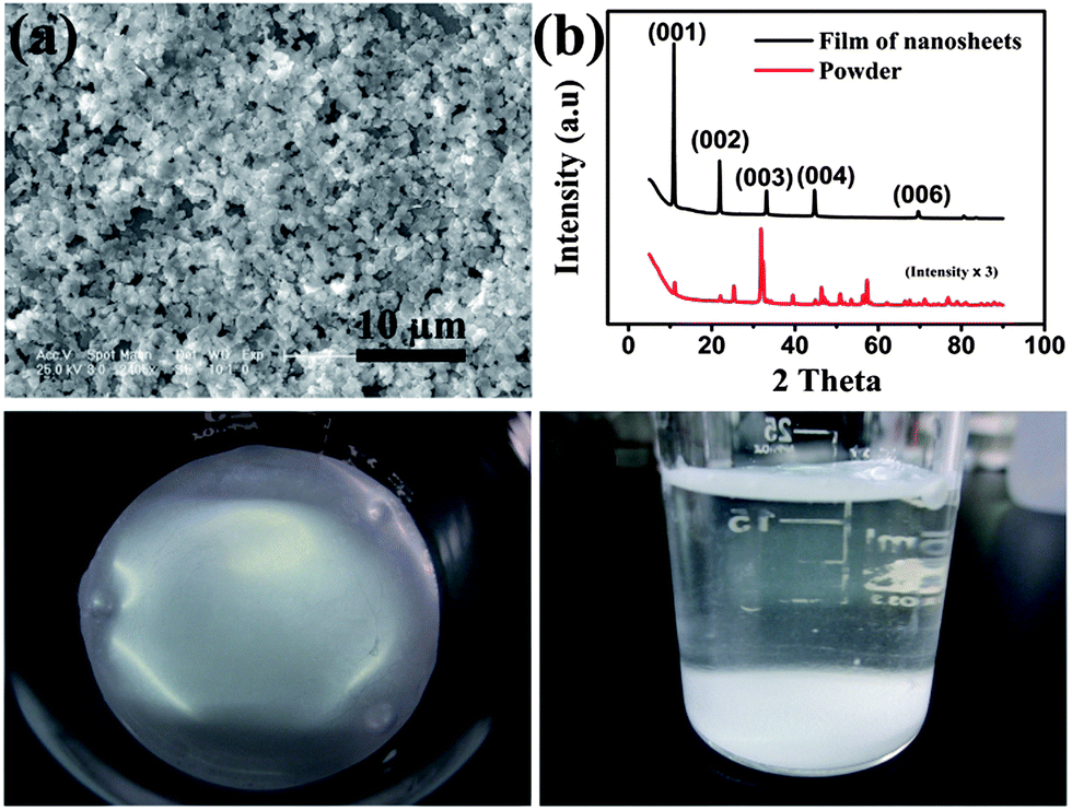 | ||
| Fig. 1 (a) SEM image of the self-assembled BiOBr film. (b) XRD patterns of the BiOBr samples. The black line represents the self-assembled film; the red line represents the powder of disordered NSs. Note that the intensity of the disordered NSs sample has been magnified by 3 times. (c and d) Digital images of the self-assembled BiOBr film in beaker. | ||
The X-ray diffraction (XRD) patterns of as-prepared BiOBr film and the powder of BiOBr NSs are displayed in Fig. 1b. All diffraction peaks of the samples can be well indexed to the tetragonal structure BiOBr (JCPDS Card no. 78-0348). The diffraction peaks of the samples are sharp and no other impurity peak is detected, indicating the high quality and purity of the samples. The highly preferred orientation of the as-assembled film also can be confirmed by the XRD patterns. Compared with the powder sample, only the (001) diffraction peaks are detected for the BiOBr film sample and the diffraction intensity is much higher than those of powder sample. These results demonstrate that the BiOBr NSs in the film are aligned parallelly to the surface of substrate with their (001) direction perpendicular to the substrate surface, which is consist with the result obtained from the SEM images. Photographs taken from the BiOBr film at water–air interface are shown in Fig. 1c and d. It is evident that a smooth and condensed BiOBr film with large area is obtained through this water–air interfacial self-assembly strategy. To further illustrate the composition, the film was characterized via energy-dispersive X-ray spectrum (EDS) and X-ray photoelectron spectroscopy (XPS). As shown in Fig. 2 and Table S1.† Bi, O and Br elements all exist, and the C and Si signals are ascribed to the substrate.
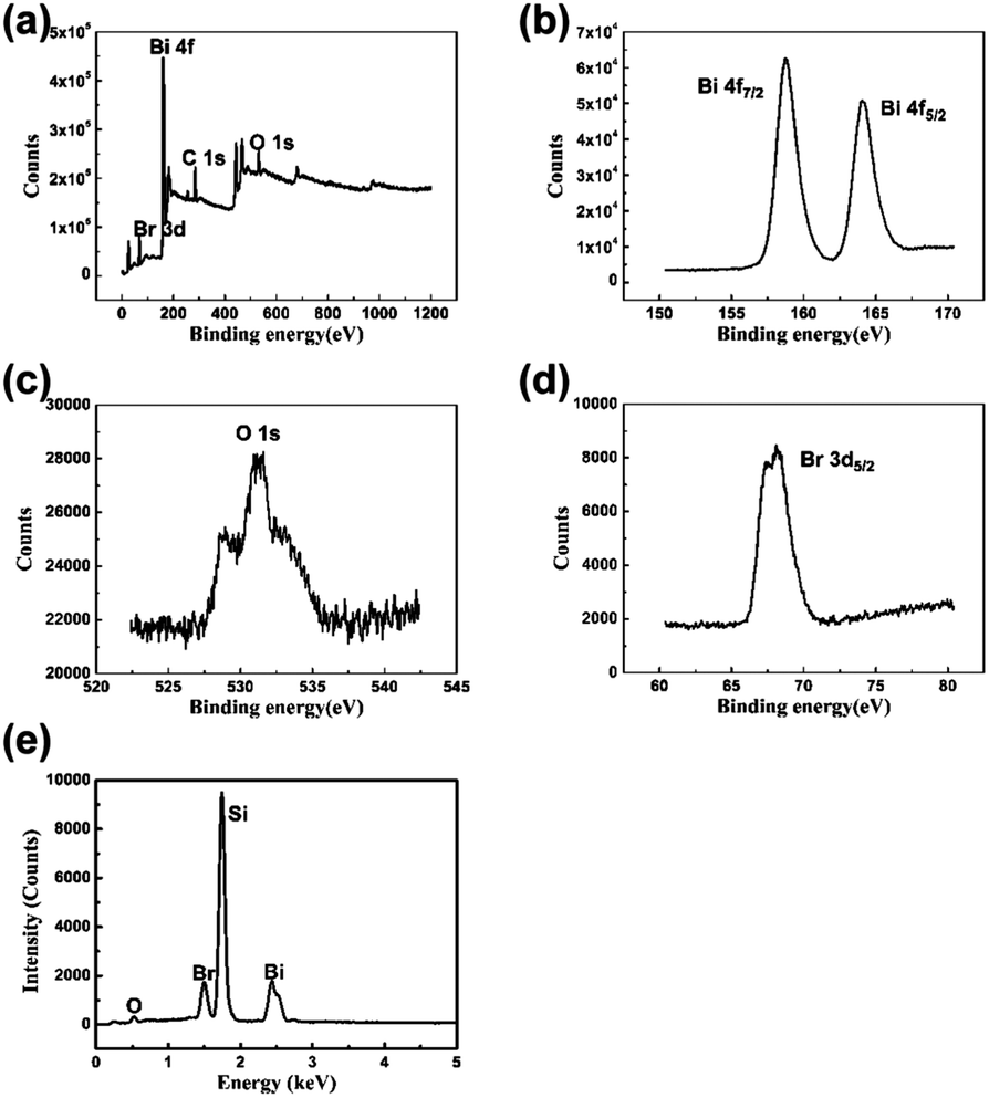 | ||
| Fig. 2 (a–d) The XPS analysis and (e) EDS spectrum of the BiOBr nanosheets. | ||
The above results suggest that this method is beneficial for fabricating large-area and highly oriented films. Accordingly, a film formation process is proposed as schematically presented in Fig. 3a. As the synthesis of the BiOBr NSs was completed, all the precipitates of the BiOBr NSs were on the bottom of the beaker after remaining stationary for a short period. Then most of the solution at the top of the beaker was carefully removed by a syringe and some deionized water was injected into the beaker. Brownian motion would happen if the particles suspended in a liquid or a gas were batted by other fast-moving particles such as water molecules. When the water was injected into the beaker, Brownian motion of BiOBr NSs was aroused by the water molecules. The NSs would have chance to arrive at the water–air interface and assemble along the interface during the injection. As the injection of water continued, more BiOBr NSs moved up to the interface and were captured by the NSs there already via van der Waals forces between them.24 Finally, a BiOBr film was formed along the water–air interface, and the film floated on the interface could be transferred onto various substrates, including glass, silicon and organic polyethylene terephthalate (PET). It is worth noting that the size of the BiOBr film is solely determined by the area of the water–air interface, and a large-area film can be easily obtained so long as a large beaker is employed. In the present experiment, the BiOBr film over a macroscopic area up to 20 cm2 is formed within 2 min. This water–air interfacial self-assembly strategy for preparing large-area film is green, convenient and rapid. In addition, all processes can be performed under ambient conditions at room temperature. These merits can offer great convenience towards large-scale production.
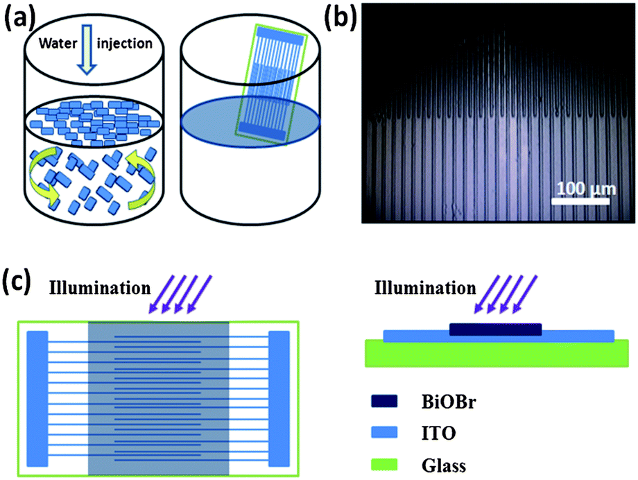 | ||
| Fig. 3 (a) Schematic representation of a proposed self-assembly process of the BiOBr film at the water–air interface and the fabrication procedure of the BiOBr film photodetector. (b) Microscope image of the interdigital electrodes configuration of the BiOBr film photodetector. (c) Schematics of the BiOBr film photodetector. | ||
The BiOBr film photodetector was constructed using ITO as the interdigital electrodes which were fabricated through a standard photolithography and etching procedure (shown in the Experimental section†). There are 100 fingers (50 up and 50 down, 5 mm long) in the interdigital structure. Fig. 3b shows a typical image of the interdigital electrodes. It can be seen that the electrode fingers are 5 μm wide with a spacing gap of 5 μm. First, the substrate with ITO interdigital electrodes was immersed into water and withdrawn at a certain angle using a RZ-1 dip coater at a constant speed. Then the BiOBr film at the water–air interface was easily transferred onto the surface of the ITO interdigital electrodes in a short time and the as-prepared device was kept in air until all water was evaporated. Fig. 3c shows the schematics of the BiOBr film photodetector.
Fig. 4a shows the absorption spectrum of BiOBr. The sample has a strong absorption to photons with wavelengths shorter than 400 nm, revealing that this material is suitable for the fabrication of UV photodetectors. The calculated band gap of the BiOBr sample is about 2.5 eV, as shown in the inset of Fig. 4a. Fig. 4b shows the current–voltage (I–V) characteristics of the BiOBr film photodetector measured in the dark and upon UV light (365 nm, 10 mW cm−2) illumination. A low dark current of 0.2 nA under a bias of 2 V is obtained. As the predominant source of noise in photodetectors, a low dark current is helpful to enhance the photodetector's signal to noise (S/N) ratio, indicating a high sensitivity and low noise. Upon UV illumination, a photocurrent of 200 nA that is 103 times larger than the dark current is detected under the same bias. It should be noted here that the I–V curves measured from the present device exhibit nonlinear behavior, indicating that there is contact barrier between the BiOBr film and the ITO electrodes. Responsivity is a critical parameter for evaluating the performance of photodetectors. The spectral responsivity of the BiOBr film photodetector under 7 V bias is plotted in Fig. 4c. Here the normalization of the responsivity (called sensitivity) is used to characterize this property of the photodetector.3,12 The absolute values of the responsivity were calculated as the ratio of photocurrent to incident illumination power at each wavelength, and the incident illumination power was obtained using a calibrated silicon photodetector. A sharp cutoff near 400 nm is observed and the maximum responsivity of the photodetector is 6 mA W−1 at 386 nm. Meanwhile, it should be noted that the R386 nm/R500 nm is about four orders of magnitude under 7 V bias, indicating that a high signal to noise (S/N) ratio and high sensitivity are achieved for the present device. Fig. 4d shows the relationship between the maximum responsivity of the photodetector and the applied bias voltage. A linear relationship is obtained between 2 and 28 V, indicating no carrier mobility saturation or sweep-out effect happens at up to 28 V bias.
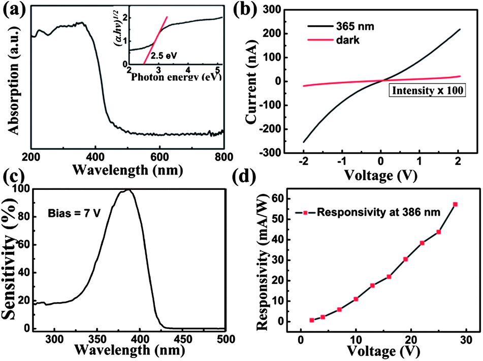 | ||
| Fig. 4 (a) Absorption spectrum of the BiOBr sample. (b) I–V characteristics of the BiOBr film photodetector illuminated with a 365 nm light and under dark conditions. Note that the dark current of the photodetector has been magnified by 100 times. (c) Spectral responsivity of the BiOBr film photodetector under 7 V bias. (d) Maximum responsivity of the BiOBr film photodetector as a function of the applied bias. | ||
For photodetectors, response speed and stability are two other important factors for practical applications. The response behavior of the BiOBr film photodetector was characterized by measuring the photocurrent as a function of time under a bias of 2 V. The photodetector could be reversibly and rapidly switched between the high and low conductivity states as the UV illumination (365 nm, 10 mW cm−2) was periodically manual chopped at about 10 s intervals, as shown in Fig. 5a. It can be seen that the photodetector exhibits highly stable and repeatable characteristics. The response time corresponded to the rise and decay processes and can be extracted from the enlarged current–time curve, as shown in Fig. 5b. Upon illumination, the photocurrent rapidly rises from 0.2 nA to 200 nA and then sharply returns to its initial value as the illumination is turned off. It can be seen that the rise and decay time are about 0.01 s, which is not the exact value due to the slow transit speed of manual chopper. In order to investigate the detailed response time of the photodetector, the UV illumination was switched on and off using a fast mechanical chopper working at 300 Hz and the output photovoltage–time relation was measured using a digital oscilloscope. The transient response of photodetector is shown in Fig. 5c and d and the periodic fluctuations of the maximum photovoltage signal is attributed to disturbance of the 50 Hz power supply. It can be observed that the rise time and decay time are estimated to be 0.67 ms and 0.8 ms, respectively, which indicates that the device shows a faster response time compared with other nanostructure-based photodetectors.25–28 Such a fast response is very desirable for practical applications in high-frequency or high-speed devices, such as optical communications or optoelectronic switches. The above results indicate that the BiOBr photodetector exhibits a fast response time and high photocurrent to dark current ratio. The comparison of the performance parameters between the present work and other photodetectors is shown in Table S2.†
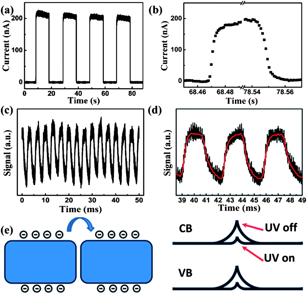 | ||
| Fig. 5 (a) Time-dependent photocurrent response to 365 nm light (10 mW cm−2) by manual chopping at about 10 s intervals. (b) The enlarged portions of the rise and decay processes of the current response. (c) A transient response by illuminating the photodetector with a 365 nm light pulse chopped at a frequency of 300 Hz. (d) An enlarged portion of the transient response of the photodetector. (e) Schematic illustration of the NS–NS junction barrier in the BiOBr film, showing a decrease in barrier height from the light-off to light-on state. | ||
For comparison, a device based on a disordered BiOBr film was also fabricated. The SEM image is shown in Fig. S3.† The disordered film is composed of powder of BiOBr NSs without a preferred orientation. As shown in Fig. S4,† although the response behavior of disordered BiOBr film photodetector is stable, the photocurrent to dark current ratio is much smaller than that of the device based on the highly orientated BiOBr film.
It is known that oxygen molecules will adsorb on the surface of nanostructures by capturing free electrons through O2(g) + e− → O2−(ad) as the nanostructure is exposed in air,29,30 creating a surface depletion layer with low conductivity. Upon light illumination, carrier density in the nanostructure increases significantly. The holes will be attracted to the surface to desorb the oxygen adsorbates through O2−(ad) + h+ → O2(g), which results in a reduction of the depletion layer thickness and an increase of the conductance. It should be noted that both the hole diffusion and oxygen adsorption–desorption processes are quite slow, which have been revealed in previous studies.17,31 For the individual nanostructure device, the resistance is determined by the nanostructure itself, thus the slow hole diffusion and oxygen adsorption–desorption processes lead to the slow response time, which is usually on the order of several minutes or hours.31 In contrast, the film of BiOBr NSs in the present device can be regarded as a network, in which the resistance is dominated by the NS–NS junction barriers.32 Therefore, a different conducting mechanism for the network device is proposed. Fig. 5e shows the schematic diagram depicting the electrical transport through the NS–NS junction barrier. It should be noted that the NS–NS junction barrier in the BiOBr film is analogous to a back-to-back Schottky barrier.32 In the present device, the electrons have to overcome the NS–NS junction barrier when tunneling from one NS to another. Upon UV illumination, the increased carrier density in BiOBr NSs will lower the barrier height since the NS–NS junction barriers are sensitive to incident illumination. It is thus easier for electron tunneling and transportation to take place, resulting in the increase in the conductivity of the NSs network.17,32,33 When the UV illumination is turned off, the carrier recombination will result in a significant increase in the barrier height due to the greatly reduced carrier density. It is generally accepted that the light-induced barrier height modulation is much faster than the hole diffusion and oxygen adsorption–desorption processes.32,33 Consequently, we suggest that the fast response time of the BiOBr film photodetector is attributed to the barrier-dominated conductivity.
To further demonstrate that the mechanism proposed for UV-detection is based on the barrier-dominated conductivity, the photocurrent as a function of time under a bias of 2 V in air, vacuum (0.5 mbar) and pure N2 were measured (shown in Fig. 6). The response time in vacuum or pure N2 is the same as that in air. The results are not consistent with the oxygen adsorption–desorption mechanism which will result in much longer rise and decay time in vacuum and pure N2 than that in air.34,35 According to the oxygen adsorption–desorption mechanism, in air the oxygen desorbed from the NSs surface is easily re-adsorbed to decrease the current by trapping electrons as the UV illumination is turned off. In vacuum and pure N2 the oxygen desorbed from the NSs surface has little chance to be re-adsorbed due to the low oxygen concentration in surrounding atmosphere. Therefore, the decay process (from photocurrent to initial dark current) can be more quickly reached in air than that in vacuum and pure N2.34,35 So the decay time in vacuum and pure N2 is much longer than that in air. The steady state of photocurrent also can be more quickly reached in air than that in vacuum and pure N2 due to the same reason. Consequently, we suggest that the mechanism proposed for UV-detection is based on the barrier-dominated conductivity rather than oxygen adsorption–desorption.
 | ||
| Fig. 6 Time-dependent photocurrent response to 365 nm light (a) in air and pure N2, 1.5 mW cm−2 (b) in air and vacuum (0.5 mbar), 0.4 mW cm−2. | ||
As shown in Fig. 6, the current measured in air is smaller than that in vacuum and pure N2. This phenomenon is attributed to the different remnant surface adsorbed oxygen in different atmospheres. Although the mechanism proposed for UV-detection is not based on the oxygen adsorption–desorption mechanism, the remnant surface adsorbed oxygen still could shorten electrons' lifetime and decrease conductivity.36 The oxygen concentration is higher in air than that in vacuum and pure N2. Therefore, more remnant surface adsorbed oxygen results in a smaller current. The intensity dependence of the photocurrent is shown in Fig. S5.† The device was irradiated with 365 nm light at power intensity ranging from 2.5 mW cm−2 to 10 mW cm−2. The results demonstrate that the photocurrent increases with light radiation, which make this device a potential quantitative photodetector.
Conclusions
In summary, a large-area BiOBr film has been prepared through a green and facile water–air interfacial self-assembly strategy, which does not have stringent requirements on the equipment and processing technique. The UV photodetector based on the BiOBr film shows low dark current, high sensitivity, a fast response time and excellent stability, indicating that the developed BiOBr film photodetector is a great candidate for applications in ultraviolet light detection. The merits of being environmentally friendly, rapid, low temperature and low cost that this strategy offers suggests an efficient route towards large-scale production of high-performance optoelectronic devices. The results also indicate that BiOBr is a promising candidate for applications in optoelectronic devices.Acknowledgements
This work was supported by the National Natural Science Foundation of China (No. 21075116) and the 973 Projects (2010CB933603, 2011CB911002). Special thanks to the wide bandgap II-VI semiconductor group (State Key Laboratory of Luminescence and Applications) for using their facilities.Notes and references
- B. J. Zeskind, C. D. Jordan, W. Timp, L. Trapani, G. Waller, V. Horodincu, D. J. Ehrlich and P. Matsudaira, Nat. Methods, 2007, 4, 567 CrossRef CAS PubMed.
- V. Formisano, S. Atreya, T. Encrenaz, N. Ignatiev and M. Giuranna, Science, 2004, 306, 1758 CrossRef CAS PubMed.
- H. Kind, H. Yan, B. Messer, M. Law and P. Yang, Adv. Mater., 2002, 14, 158 CrossRef CAS.
- D. Li, X. Sun, H. Song, Z. Li, Y. Chen, H. Jiang and G. Miao, Adv. Mater., 2012, 24, 845 CrossRef CAS PubMed.
- (a) F. Guo, B. Yang, Y. Yuan, Z. Xiao, Q. Dong, Y. Bi and J. Huang, Nat. Nanotechnol., 2012, 7, 798 CrossRef CAS PubMed; (b) L. Hu, M. Chen, W. Shan, T. Zhan, M. Liao, X. Fang, X. Hu and L. Wu, Adv. Mater., 2012, 24, 5872–5877 CrossRef CAS PubMed; (c) X. Wang, M. Liao, Y. Zhong, J. Y. Zheng, W. Tian, T. Zhai, C. Zhi, Y. Ma, J. Yao, Y. Bando and D. Golberg, Adv. Mater., 2012, 24, 3421–3425 CrossRef CAS PubMed.
- (a) G. Konstantatos and E. H. Sargent, Nat. Nanotechnol., 2010, 5, 391 CrossRef CAS PubMed; (b) W. Tian, C. Zhang, T. Zhai, S.-L. Li, X. Wang, M. Liao, K. Tsukagoshi, D. Golberg and Y. Bando, Chem. Commun., 2013, 49, 3739–3741 RSC; (c) W. Tian, T. Zhai, C. Zhang, S.-L. Li, X. Wang, F. Liu, D. Liu, X. Cai, K. Tsukagoshi, D. Golberg and Y. Bando, Adv. Mater., 2013, 25, 4625–4630 CrossRef CAS PubMed.
- Y. Liu, C. R. Gorla, S. Liang, N. Emanetoglu, Y. Lu, H. Shen and M. Wraback, J. Electron. Mater., 2000, 29, 69 CrossRef CAS PubMed.
- S. Liang, H. Sheng, Y. Liu, Z. Huo, Y. Lu and H. Shen, J. Cryst. Growth, 2001, 225, 110 CrossRef CAS.
- G. Y. Xu, A. Salvador, W. Kim, Z. Fan, C. Lu, H. Tang, H. Morkoc, G. Smith, M. Estes, B. Goldenberg, W. Yang and S. Krishnankutty, Appl. Phys. Lett., 1997, 71, 2154 CrossRef CAS.
- G. Parish, S. Keller, P. Kozodoy, J. P. Ibbetson, H. Marchand, P. T. Fini, S. B. Fleischer, S. P. DenBaars, U. K. Mishra and E. J. Tarsa, Appl. Phys. Lett., 1999, 75, 247 CrossRef CAS.
- X. W. Fu, Z. M. Liao, J. Xu, X. S. Wu, W. l. Guo and D. P. Yu, Nanoscale, 2013, 5, 916 RSC.
- (a) L. F. Hu, J. Yan, M. Y. Liao, H. J. Xiang, X. G. Gong, L. D. Zhang and X. S. Fang, Adv. Mater., 2012, 24, 2305 CrossRef CAS PubMed; (b) J. Pan, J. Li, Z. Yan, B. Zhou, H. Wu and X. Xiong, Nanoscale, 2013, 5, 3022–3029 RSC.
- Z. Guo, D. Zhao, Y. Liu, D. Shen, J. Zhang and B. Li, Appl. Phys. Lett., 2008, 93, 163501 CrossRef.
- (a) L. Hu, M. Chen, X. Fang and L. Wu, Chem. Soc. Rev., 2012, 41, 1350 RSC; (b) Y. Ren, M. Chen, L. Hu, X. Fang and L. Wu, J. Mater. Chem., 2012, 22, 944–950 RSC.
- F. Reincke, S. G. Hickey, W. K. Kegel and D. Vanmaekelbergh, Angew. Chem., Int. Ed., 2004, 43, 458 CrossRef CAS PubMed.
- H. Xia and D. Wang, Adv. Mater., 2008, 20, 4253 CrossRef CAS.
- M. Chen, L. Hu, J. Xu, M. Liao, L. Wu and X. Fang, Small, 2011, 7, 2449 CAS.
- L. Hu, L. Wu, M. Liao and X. Fang, Adv. Mater., 2011, 23, 1988 CrossRef CAS PubMed.
- S. Shenawi-Khalil, V. Uvarov, S. Fronton, I. Popov and Y. Sasson, J. Phys. Chem. C, 2012, 116, 11004 CAS.
- J. Zhang, F. Shi, J. Lin, D. Chen, J. Gao, Z. Huang, X. Ding and C. Tang, Chem. Mater., 2008, 20, 2937 CrossRef CAS.
- H. Cheng, B. Huang, Z. Wang, X. Qin, X. Zhang and Y. Dai, Chem.–Eur. J., 2011, 17, 8039 CrossRef CAS PubMed.
- L. Kong, Z. Jiang, T. Xiao, L. Lu, M. O. Jones and P. P. Edwards, Chem. Commun., 2011, 47, 5512 RSC.
- H. Cheng, B. Huang, P. Wang, Z. Wang, Z. Lou, J. Wang, X. Qin, X. Zhang and Y. Dai, Chem. Commun., 2011, 47, 7054 RSC.
- C. Chen, Q.-H. Yang, Y. Yang, W. Lv, Y. Wen, P.-X. Hou, M. Wang and H.-M. Cheng, Adv. Mater., 2009, 21, 3007 CrossRef CAS.
- Y. Jin, J. Wang, B. Sun, J. C. Blakesley and N. C. Greenham, Nano Lett., 2008, 8, 1649 CrossRef CAS PubMed.
- S. Nath Das, K. J. Moon, J. P. Kar, J. H. Choi, J. Xiong, T. I. Lee and J. M. Myoung, Appl. Phys. Lett., 2010, 97, 022103 CrossRef.
- Y. Yang, W. Guo, J. Qi, J. Zhao and Y. Zhang, Appl. Phys. Lett., 2010, 97, 223113 CrossRef.
- H. Wu, Y. Sun, D. Lin, R. Zhang, C. Zhang and W. Pan, Adv. Mater., 2009, 21, 227 CrossRef CAS.
- C. Soci, A. Zhang, B. Xiang, S. A. Dayeh, D. P. R. Aplin, J. Park, X. Y. Bao, Y. H. Lo and D. Wang, Nano Lett., 2007, 7, 1003 CrossRef CAS PubMed.
- Y. H. Ahn and J. Park, Appl. Phys. Lett., 2007, 91, 162102 CrossRef.
- K. Liu, M. Sakurai, M. Liao and M. Aono, J. Phys. Chem. C, 2010, 114, 19835 CAS.
- C. Yan, N. Singh and P. S. Lee, Appl. Phys. Lett., 2010, 96, 053108 CrossRef.
- C. Yan, N. Singh, H. Cai, C. L. Gan and P. S. Lee, ACS Appl. Mater. Interfaces, 2010, 2, 1794 CAS.
- Q. H. Li, T. Gao, Y. G. Wang and T. H. Wang, Appl. Phys. Lett., 2005, 86, 123117 CrossRef.
- K. Pomoni, A. Vomvas and C. Trapalis, J. Non-Cryst. Solids, 2008, 354, 4448 CrossRef CAS PubMed.
- A. M. Eppler, I. M. Ballard and J. Nelson, Physica E: Low-dimensional Systems and Nanostructures, 2002, 14, 197 CrossRef CAS.
Footnote |
| † Electronic supplementary information (ESI) available: (i) Experimental details on NS synthesis and device fabrication; (ii) TEM, SEM, AFM images and EDS analysis of NS; (iii) I–V curves under different light intensities. See DOI: 10.1039/c3nr04496c |
| This journal is © The Royal Society of Chemistry 2014 |