Penetration and lateral diffusion characteristics of polycrystalline graphene barriers†
Taeshik
Yoon
a,
Jeong Hun
Mun
b,
Byung Jin
Cho
*bc and
Taek-Soo
Kim
*ac
aDepartment of Mechanical Engineering, KAIST, Daejeon 305-701, Korea. E-mail: tskim1@kaist.ac.kr
bDepartment of Electrical Engineering, KAIST, Daejeon 305-701, Korea. E-mail: bjcho@ee.kaist.ac.kr
cGraphene Research Center (GRC), KAIST, Daejeon 305-701, Korea
First published on 22nd October 2013
Abstract
We report penetration and lateral diffusion behavior of environmental molecules on synthesized polycrystalline graphene. Penetration occurs through graphene grain boundaries resulting in local oxidation. However, when the penetrated molecules diffuse laterally, the oxidation region will expand. Therefore, we measured the lateral diffusion rate along the graphene–copper interface for the first time by the environment-assisted crack growth test. It is clearly shown that the lateral diffusion is suppressed due to the high van der Waals interaction. Finally, we employed bilayer graphene for a perfect diffusion barrier facilitated by decreased defect density and increased lateral diffusion path.
Graphene has been regarded as a superior diffusion barrier1–5 due to its atomic structure, which is composed of densely packed carbon atoms.6–8 Synthesized graphene2,3 and rGO (reduced graphene oxide) multilayers1,4,9 have been adopted as gas diffusion barriers, which showed extremely high resistance to molecular penetration. As barrier layers, graphene provides additional advantages in real applications. One-atom-thickness overcomes dimension constraints from an engineering perspective, and transparency enables optical applications. Furthermore, extremely low bending stiffness ensures conformal contact with arbitrary surfaces. Large-area graphene10–13 synthesized for the purpose of a diffusion barrier is basically polycrystalline, and therefore has numerous graphene grain boundaries (GGBs).14–19 However, these GGBs are potentially vulnerable to the penetration of molecules because their chemical structures are modified, with larger vacancies or non-carbon atoms.19,20 It has been reported that the modified GGB structure significantly reduces the activation energy of diffusion,19 and as a result, metal oxidation occurs since environmental molecules such as oxygen or water will tend to penetrate into the graphene membrane. GGBs are critical defects, which should be considered before using graphene as a diffusion barrier. Furthermore, lateral diffusion of the penetrating molecules along the interface between graphene and metal is also a critical concern. Once lateral diffusion occurs, oxidation along the interface will be accelerated, which will further lead to delamination of the graphene barrier from the metal.21,22 Although it is known that a graphene surface enables the ultrafast diffusion of water molecules even at low temperature,23,24 a recent study showed that water molecules can be stably trapped at the interface between graphene and mica, which implies that lateral diffusion is unfavorable.25 To the best of our knowledge, an investigation of the lateral diffusion of penetrating environmental molecules between as-grown graphene and copper, which is critical for the passivation, has not been reported.
Here, we show the penetration of molecules on GGBs and their lateral diffusion along the graphene–metal interface. To visualize GGBs on the metal, as-grown graphene on the metal was heated, and the temperature dependent oxidation of the metal on GGBs was observed. Monolayer and bilayer graphene were utilized for metal passivation, and the bilayer graphene on the metal showed superior resistance to oxidation when compared with that of monolayer graphene. The lateral diffusion of molecules between graphene and metal was measured by the environment-assisted crack growth test.26–29 Through these analyses, the barrier mechanism of graphene is explained, and we discuss why graphene is still a superior diffusion barrier even though it has numerous GGBs.
To visualize GGBs, as-grown graphene on the metal was heated to induce metal oxidation. The test procedure is shown in Fig. 1. A 300 nm thick copper film was deposited on a silicon wafer, and then graphene was synthesized by the chemical vapor deposition (CVD) method.29 The scanning electron microscope (SEM) image in Fig. 1a shows the as-grown graphene on copper, and the copper has grains of a few-micron-size. As shown in Fig. 1b, the graphene on the metal was then heated in controlled lab air containing oxygen and water molecules. We observed that no meaningful changes appeared in the SEM images until heating reached 100 °C. However, when the temperature was over 150 °C, bright lines formed on the surface of the graphene, as shown in the SEM image of Fig. 1b. The bright lines are metal oxide which grew at the GGBs following the penetration of molecules. This result clearly shows that molecules can easily penetrate into the GGBs, and react with the metal at high temperature. Therefore, even though graphene is a superior oxidation barrier, GGBs are vulnerable to molecular diffusion.
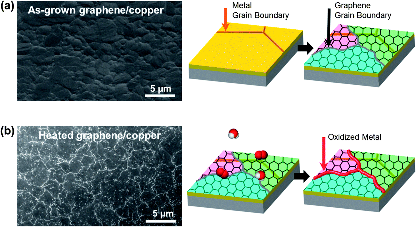 | ||
| Fig. 1 Visualizing graphene grain boundaries by heating graphene on a metal. (a) SEM image of the as-grown graphene on copper. (b) SEM image of the heated graphene on copper. The bright lines are metal oxide formed on GGBs by penetration of environmental molecules. | ||
The key issue in visualizing GGBs is determining whether the formed lines are GGBs or metal grain boundaries. We used atomic force microscopy (AFM) for morphology mapping of the heated multilayer. Representative AFM images of the heated graphene–copper surface are shown in Fig. 2. Fig. 2a and b show low-magnification topography and high-magnification phase images, respectively. The metal grain boundaries can be observed as the dark and concave lines in Fig. 2a and c, while metal oxide lines are bright and convex. The lines formed on GGBs are connected with other lines, and Fig. 2c shows the junction of triple GGBs. The junction exists on a single grain of the metal, and the line profiles of Fig. 2c are shown in Fig. 2d. From these results, it can be clearly seen that the formed metal lines do not coincide with the metal grain boundaries. Therefore, the oxidized lines formed on GGBs are independent of the location and shape of metal grain boundaries. These results agree with recent research about the relationship of GGBs and metal grain boundaries.19
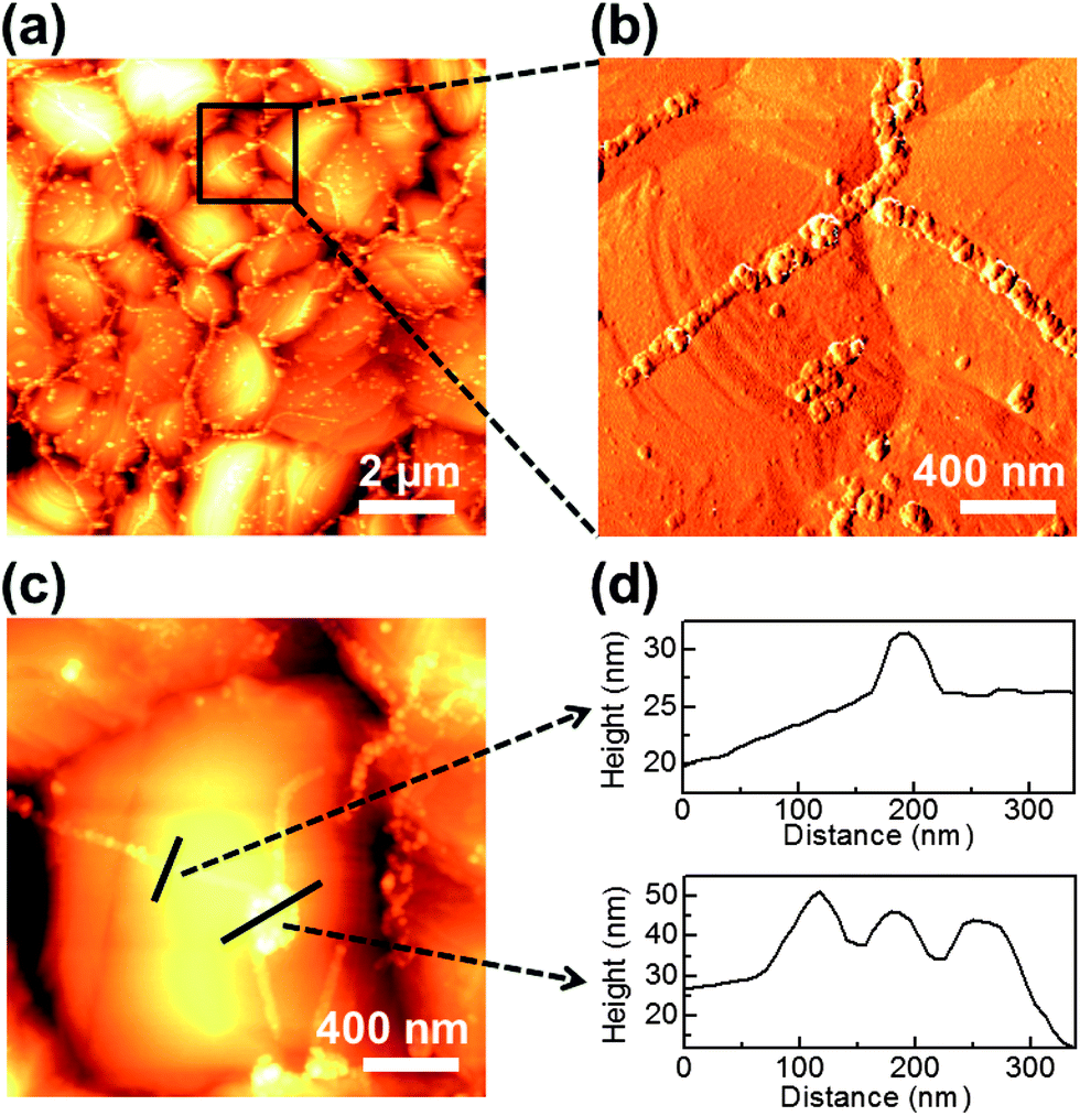 | ||
| Fig. 2 Morphology mapping of the metal oxide lines on graphene grain boundaries by AFM. (a) Low-magnification topography image showing the visualized GGBs on the metal. (b) High-magnification phase image showing that the location of GGBs is independent of the metal grain boundaries. (c) High-magnification topography image showing that triple GGBs are connected on a single metal grain. (d) Height profiles of the formed metal oxide lines marked in (c). | ||
To observe the effect of temperature on metal passivation, our heating temperature was varied from 150 °C to 200 °C. Fig. 3a–c show that the metal oxide lines on GGBs get thicker as the heating temperature increases. Fig. 3d and e show the width and height of the formed lines, which were measured by AFM profiling. As in the SEM images, the line width and height are strongly dependent on the heating temperature. High temperature enhanced penetration of environmental molecules through GGBs can be well explained by a thermally activated diffusion process.
 | ||
| Fig. 3 Evolution of the metal oxide lines with temperature. SEM images of the heated graphene on copper (a–c). The heating temperatures are 150 °C (a), 175 °C (b) and 200 °C (c). The dimensions of the lines are measured by AFM (d and e). The width (d) and height (e) of the oxidized metal lines are plotted. | ||
Synthesized large-area graphene has numerous GGBs on the plane, and these become line defects during metal passivation. To obtain higher passivation performance with graphene, we propose a method of stacking bilayer graphene on the metal to minimize these defects. While graphene is composed of line defects, when another graphene layer is added to the surface, only point defects can occur at the intersection of line defects from two separate graphene layers. Therefore, this method effectively reduces penetration of the environmental molecules. Furthermore, a longer diffusion path is required for environmental molecules to reach the metal; hence oxidation can be retarded.
Bare copper, monolayer graphene on copper, and bilayer graphene on copper were prepared to evaluate metal passivation. The bilayer sample was prepared by transferring monolayer graphene onto an already grown monolayer graphene–metal specimen.11,13 The number of graphene layers was reconfirmed by Raman spectra.30 As shown in Fig. 4d, the peak intensities of G and 2D are almost the same in the bilayer graphene, while the 2D peak is stronger than the G peak in the monolayer graphene. Same heating conditions of 200 °C and 3 minutes were used for each sample. Fig. 4a shows the bare metal without graphene: the entire metal surface is covered by metal oxide and the metal's original morphology has disappeared. In the case of monolayer graphene on copper, it can effectively block oxidation except for the GGB region, as shown in Fig. 4b. However, the results of the bilayer graphene sample in Fig. 4c do not show any oxidized area. This means that the metal is perfectly protected by the bilayer graphene by increased lateral diffusion path and reduced defect sites. This result is notably promising because the deleterious effects of GGBs in polycrystalline graphene can be simply eliminated by just adding a graphene layer, which does not impede the advantages of using graphene.
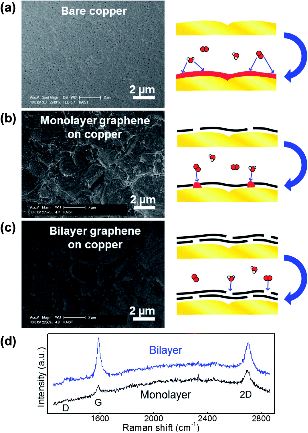 | ||
| Fig. 4 Stacking graphene layers for metal passivation. SEM images after heating (a–c). The specimen structures are bare copper (a), monolayer graphene on copper (b) and bilayer graphene on copper (c). The bilayer graphene can effectively block the environmental molecules, while oxidized metal lines are formed on GGBs in the monolayer graphene specimen. (d) Raman spectra of monolayer and bilayer graphene on copper. | ||
So far, the penetration of molecules into the graphene membrane has been addressed; however, lateral diffusion along the graphene–metal interface should also be considered for a better understanding of the passivation mechanism. We found that the environmental molecules can easily penetrate into the graphene membrane via GGBs, even though graphene has superior impermeability. Furthermore, if the penetrated molecules are mobile on the graphene–metal interface, oxidation will be accelerated and the passivation will be eventually useless. For this reason, lateral diffusion should be quantitatively measured and studied. However, it has not been previously reported because of the difficulty of accurately controlling the interface.
In our study, the graphene–metal interface was mechanically opened for measurement of the lateral diffusion rate by an environment-assisted crack growth test. The lateral diffusion of molecules gives rise to interface debonding, and finally a crack is propagated. The lateral diffusion rate is equivalent to the crack growth rate, which can be measured by the environment-assisted crack growth test.26–28 The specimen structure29 is shown in the inset of Fig. 5a, and further information is provided in the environment-assisted crack growth test discussion in the Experimental section. The test conditions were RH (Relative Humidity) values of 50%, 70% and 90% with a fixed temperature of 30 °C.
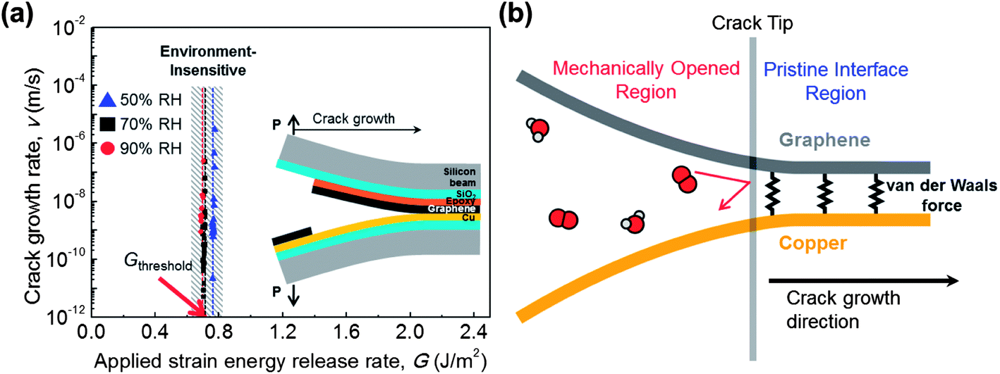 | ||
| Fig. 5 Lateral diffusion of environmental molecules along the graphene–copper interface. (a) Environment-assisted crack growth test of the graphene–copper interface. The crack growth rate is measured as a function of the applied strain energy release rate. The specimen structure is shown in the inset. The threshold G is equal to the adhesion energy of the interface, which means that the lateral diffusion hardly occurs unless the interface is mechanically opened. (b) Atomic-scale schematic of the crack tip. The molecules can freely diffuse through the mechanically opened region while the van der Waals force of graphene suppresses lateral diffusion along the pristine interface. | ||
The crack growth rate was measured with the applied strain energy release rate as shown in Fig. 5a. The applied strain energy release rate (G) is the factor of loading condition at the crack tip, which is related to crack length, dimensions, and applied load. The threshold G is determined when the crack starts to propagate, which was found to be 0.7 J m−2. This value exactly corresponds to the adhesion energy of graphene–copper,29 which indicates that the crack growth was not affected by environmental molecules;27 therefore there was no meaningful difference for the three RH conditions. The measured minimum crack growth rate was 10−11 m s−1, which is the lower limit of our measurement system. This means that the lateral diffusion rate will be lower than 10−11 m s−1 when the G is lower than the energy of graphene–copper. In other words, the environmental molecules hardly diffuse unless the interface is mechanically opened, and do not affect the adhesion energy of graphene–copper. To the best of our knowledge, this is the first reported measurement of lateral diffusion between as-grown graphene on copper, and it reveals the lateral diffusion suppressing ability of graphene. It has been reported that lateral diffusion along the graphene oxide layers yields a rate on the order of 10−4 m s−1 (ref. 31), which is seven orders of magnitude higher than our result, 10−11 m s−1. This comparison clearly suggests that the as-grown graphene on the metal is truly an ideal barrier to lateral diffusion. The suppression of lateral diffusion can also be confirmed by the previous study which found that water molecules become immobile between pristine graphene and mica.25
The atomic-scale schematic of the crack tip is shown in Fig. 5b. Although environmental molecules can freely diffuse into a mechanically opened region, they hardly diffuse into a pristine interface region. The graphene effectively impedes the lateral diffusion of molecules because the high van der Waals interaction between graphene and metal29,32 results in a high activation energy for the lateral diffusion of molecules. According to the previous results discussed in this paper, the suppressed lateral diffusion plays an important role in metal passivation. Experimental results clearly show that the suppressed lateral diffusion prevents further spreading of the oxidation region, although the penetration of molecules occurs on GGBs in monolayer graphene. Furthermore, bilayer graphene can eliminate this penetration by increasing lateral diffusion path and reducing defect sites.
In conclusion, we have characterized the penetration and lateral diffusion of polycrystalline graphene used as a diffusion barrier. Graphene defects were visualized by the penetration of molecules on GGBs, a method which can be used directly for evaluating synthesized graphene. Even though the GGBs enabled metal oxidation, it was arrested by stacking bilayer graphene. The measured lateral diffusion rate along the as-grown graphene–copper interface was lower than that of the graphene oxide interface by seven orders of magnitude, which reveals that polycrystalline graphene is still an ideal diffusion barrier.
Experimental section
Graphene synthesis and sample preparation
Graphene layers were synthesized by the CVD method.10,11,33 For the catalytic substrate, a Cu (300 nm) thin film was deposited sequentially on an oxidized silicon wafer. After the in situ cleaning process of H2 plasma annealing, the sample was annealed at 700 °C for 2 min. The pressure was maintained at 50 mTorr, and the precursor gases were Ar![[thin space (1/6-em)]](https://www.rsc.org/images/entities/char_2009.gif) :C2H2 = 40:1. For the preparation of bilayer graphene on a Cu thin film, one graphene layer was transferred onto another graphene grown Cu sample by a wet transfer method.33,34
:C2H2 = 40:1. For the preparation of bilayer graphene on a Cu thin film, one graphene layer was transferred onto another graphene grown Cu sample by a wet transfer method.33,34
Environment-assisted crack growth test
The specimen structure is based on the double cantilever beam (DCB) test, which enables symmetric beam bending. A graphene–Cu–silicon wafer was prepared, and a same size dummy silicon wafer was also prepared. The epoxy adhesive (Epo-Tek 353nd) was used for bonding both wafer beams, and was cured in a convection oven. Aluminum loading tabs were attached on each side of beams for coupling the specimen with the micromechanical test system (Delaminator Adhesion Test System; DTS Company), which is composed of linear actuator and load-cell. The whole system was then put into an environmental chamber with controlled temperature and humidity. The crack can be propagated by tensile motion of the linear actuator. After initial crack propagation, the load relaxation was measured while the displacement was fixed. The load decreased with crack propagation; the crack growth rate can be measured as a function of the applied strain energy release rate as shown in Fig. 5a.Surface characterization methods
For the characterization of graphene on the metal, we utilized Raman spectroscopy. The ARAMIS (Horiba Jobin Yvon, France) equipment was used, and an Ar ion laser beam (514.5 nm) was irradiated on graphene–Cu surfaces. The obtained spectrum ranged from 1000 cm−1 to 3000 cm−1, and each spectrum was acquired twenty times. A field-emission scanning electron microscope (FE-SEM) was used for visualizing metal oxidation. The 10 kV electron beam with 22500× magnification was used to observe oxidized metal lines of sub-micron thickness. Finally, the morphology of visualized metal oxide lines was characterized using atomic force microscopy (XE-100, Park Systems, Korea). The topography and phase images were obtained using non-contact mode, and the 100 μm2 area was scanned on each sample.
Acknowledgements
This work was supported by National Research Foundation of Korea (NRF) Research Grants 2012-R1A1A1006072, 2013-H1A2A1032731, 2010-0029132, and 2011-0031638.References
- H. Kim, Y. Miura and C. W. Macosko, Chem. Mater., 2010, 22, 3441–3450 CrossRef CAS
.
- E. Sutter, P. Albrecht, F. E. Camino and P. Sutter, Carbon, 2010, 48, 4414–4420 CrossRef CAS PubMed
- S. Chen, L. Brown, M. Levendorf, W. Cai, S.-Y. Ju, J. Edgeworth, X. Li, C. W. Magnuson, A. Velamakanni and R. D. Piner, ACS Nano, 2011, 5, 1321–1327 CrossRef CAS PubMed
- L. Qiu, X. Zhang, W. Yang, Y. Wang, G. P. Simon and D. Li, Chem. Commun., 2011, 47, 5810–5812 RSC
- F. Guo, G. Silverberg, S. Bowers, S.-P. Kim, D. Datta, V. Shenoy and R. H. Hurt, Environ. Sci. Technol., 2012, 46, 7717–7724 CrossRef CAS PubMed
- K. Novoselov, A. K. Geim, S. Morozov, D. Jiang, Y. Zhang, S. Dubonos, I. Grigorieva and A. Firsov, Science, 2004, 306, 666–669 CrossRef CAS PubMed
- A. K. Geim and K. S. Novoselov, Nat. Mater., 2007, 6, 183–191 CrossRef CAS PubMed
- J. S. Bunch, S. S. Verbridge, J. S. Alden, A. M. van der Zande, J. M. Parpia, H. G. Craighead and P. L. McEuen, Nano Lett., 2008, 8, 2458–2462 CrossRef CAS PubMed
- H. M. Kim, J. K. Lee and H. S. Lee, Thin Solid Films, 2011, 519, 7766–7771 CrossRef CAS PubMed
- A. Reina, X. Jia, J. Ho, D. Nezich, H. Son, V. Bulovic, M. S. Dresselhaus and J. Kong, Nano Lett., 2008, 9, 30–35 CrossRef PubMed
- K. S. Kim, Y. Zhao, H. Jang, S. Y. Lee, J. M. Kim, K. S. Kim, J.-H. Ahn, P. Kim, J.-Y. Choi and B. H. Hong, Nature, 2009, 457, 706–710 CrossRef CAS PubMed
- X. Li, W. Cai, J. An, S. Kim, J. Nah, D. Yang, R. Piner, A. Velamakanni, I. Jung and E. Tutuc, Science, 2009, 324, 1312–1314 CrossRef CAS PubMed
- S. Bae, H. Kim, Y. Lee, X. Xu, J.-S. Park, Y. Zheng, J. Balakrishnan, T. Lei, H. R. Kim and Y. I. Song, Nat. Nanotechnol., 2010, 5, 574–578 CrossRef CAS PubMed
- R. Grantab, V. B. Shenoy and R. S. Ruoff, Science, 2010, 330, 946–948 CrossRef CAS PubMed
- O. V. Yazyev and S. G. Louie, Nat. Mater., 2010, 9, 806–809 CrossRef CAS PubMed
- P. Y. Huang, C. S. Ruiz-Vargas, A. M. van der Zande, W. S. Whitney, M. P. Levendorf, J. W. Kevek, S. Garg, J. S. Alden, C. J. Hustedt and Y. Zhu, Nature, 2011, 469, 389–392 CrossRef CAS PubMed
- D. W. Kim, Y. H. Kim, H. S. Jeong and H.-T. Jung, Nat. Nanotechnol., 2011, 7, 29–34 CrossRef PubMed
- K. Kim, Z. Lee, W. Regan, C. Kisielowski, M. Crommie and A. Zettl, ACS Nano, 2011, 5, 2142–2146 CrossRef CAS PubMed
- D. L. Duong, G. H. Han, S. M. Lee, F. Gunes, E. S. Kim, S. T. Kim, H. Kim, Q. H. Ta, K. P. So and S. J. Yoon, Nature, 2012, 490, 235–239 CrossRef CAS PubMed
- M. E. Suk and N. Aluru, J. Phys. Chem. Lett., 2010, 1, 1590–1594 CrossRef CAS
- P. A. Sørensen, K. Dam-Johansen, C. Weinell and S. Kiil, Prog. Org. Coat., 2010, 67, 107–115 CrossRef PubMed
- P. Sutter, J. T. Sadowski and E. A. Sutter, J. Am. Chem. Soc., 2010, 132, 8175–8179 CrossRef CAS PubMed
- J. Ma, A. Michaelides, D. Alfe, L. Schimka, G. Kresse and E. Wang, Phys. Rev. B: Condens. Matter Mater. Phys., 2011, 84, 033402 CrossRef
- J. H. Park and N. Aluru, J. Phys. Chem. C, 2010, 114, 2595–2599 CAS
- K. Xu, P. Cao and J. R. Heath, Science, 2010, 329, 1188–1191 CrossRef CAS PubMed
- S. Wiederhorn, J. Am. Ceram. Soc., 1967, 50, 407–414 CrossRef CAS
- T. A. Michalske and B. C. Bunker, J. Am. Ceram. Soc., 1987, 70, 780–784 CrossRef CAS
- R. Dauskardt, M. Lane, Q. Ma and N. Krishna, Eng. Fract. Mech., 1998, 61, 141–162 CrossRef
- T. Yoon, W. C. Shin, T. Y. Kim, J. H. Mun, T.-S. Kim and B. J. Cho, Nano Lett., 2012, 12, 1448–1452 CrossRef CAS PubMed
- A. Ferrari, J. Meyer, V. Scardaci, C. Casiraghi, M. Lazzeri, F. Mauri, S. Piscanec, D. Jiang, K. Novoselov and S. Roth, Phys. Rev. Lett., 2006, 97, 187401 CrossRef CAS
- R. Nair, H. Wu, P. Jayaram, I. Grigorieva and A. Geim, Science, 2012, 335, 442–444 CrossRef CAS PubMed
- S. P. Koenig, N. G. Boddeti, M. L. Dunn and J. S. Bunch, Nat. Nanotechnol., 2011, 6, 543–546 CrossRef CAS PubMed
- J. H. Mun and B. J. Cho, Nano Lett., 2013, 13, 2496–2499 CrossRef CAS PubMed
- X. Li, Y. Zhu, W. Cai, M. Borysiak, B. Han, D. Chen, R. D. Piner, L. Colombo and R. S. Ruoff, Nano Lett., 2009, 9, 4359–4363 CrossRef CAS PubMed
Footnote |
| † Electronic supplementary information (ESI) available. See DOI: 10.1039/c3nr03849a |
| This journal is © The Royal Society of Chemistry 2014 |